
Substrate for and a process in connection with the product of structures
a technology of substrate and product, applied in the direction of individual molecule manipulation, fluid speed measurement, optical light guide, etc., can solve the problems of uneven structure on the substrate, structural variations in the surface material of the flat plate, uneven surface embedding,
Patent Information
- Authority / Receiving Office
- US · United States
- Current Assignee / Owner
- Publication Date
- 2004-01-08
- Estimated Expiration
- Not applicable · inactive patent
Smart Images
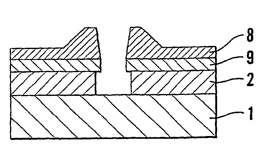
Figure 1 
Figure 2 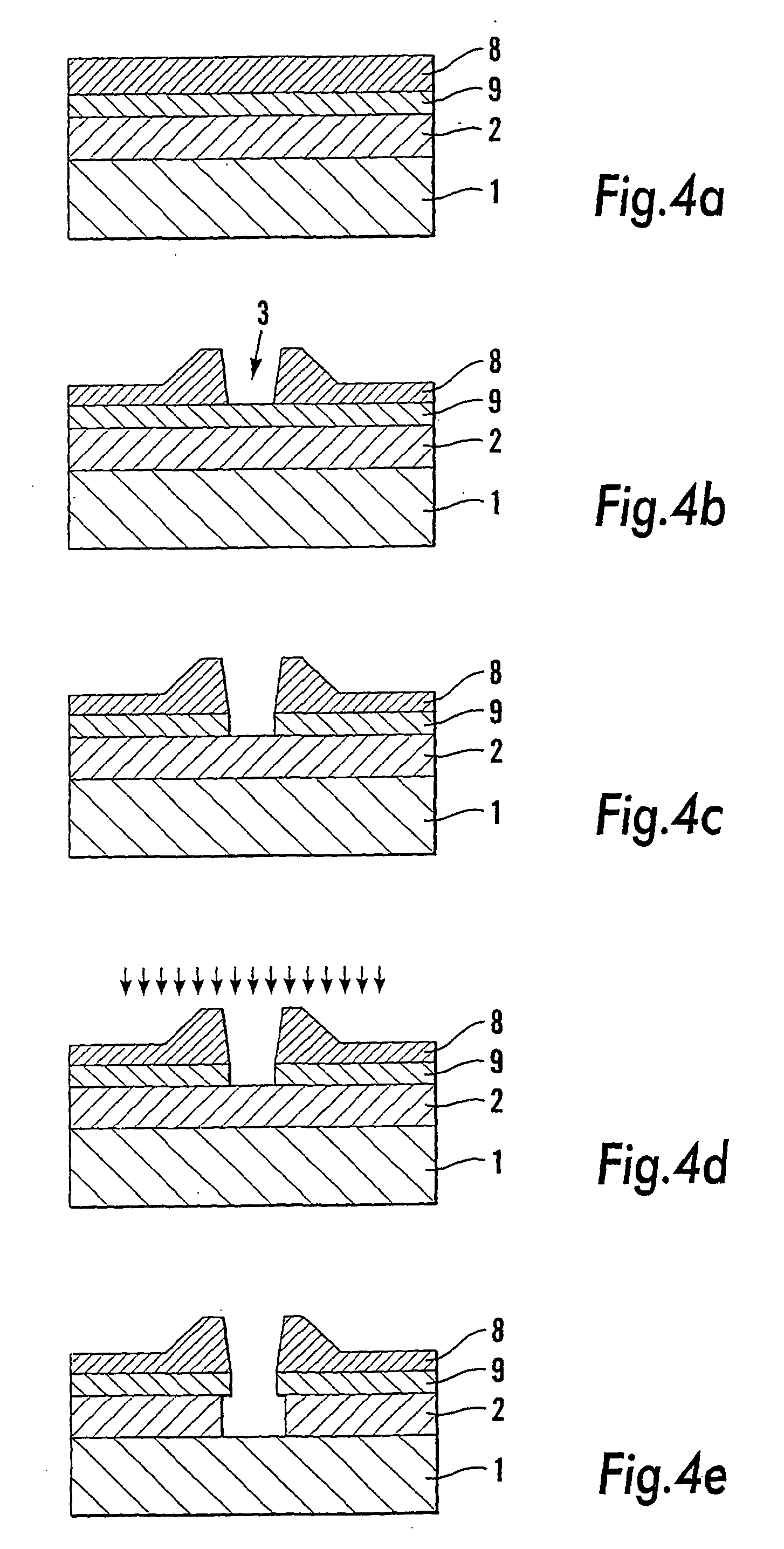
Figure 3
Abstract
Description
[0001] The present invention relates to a substrate including at least a first and a second coating layer on one surface of the substrate, for nanoimprint lithography.
[0002] The invention also relates to a process in connection with the lithography of structures of nanometre size on a coated substrate. The invention is applicable in connection with nanoimprint lithography on semiconductor materials, such as silicon, indium phosphide or gallium arsenide, for the production of semiconductor components, but also in connection with nanoimprint lithography on other rigid materials, such as ceramic materials, metals or polymers with a relatively high glass transition temperature, for use in e.g. biosensors.PRIOR ART
[0003] The trend in microelectronics is towards ever smaller dimensions. In principle, development has been such that the dimensions are halving every third year. Commercial components are being manufactured today with structures of roughly 200 nm in size, but there is a need t...
Examples
first embodiment
[0033] FIGS. 4a-e show a coated substrate according to the invention and the stages for NIL of the same,
second embodiment
[0034] FIGS. 5a-c show a coated substrate according to the invention and the stages for NIL of the same,
third embodiment
[0035] FIGS. 6a-d show a coated substrate according to the invention and the stages for NIL of the same,
[0036] FIG. 7 shows a preferred device, seen from the side in cross-section, for execution of the imprint stage,
[0037] FIG. 8a shows a scanning electron microscope image of a coated, nanoimprinted and developed substrate according to the invention,
[0038] FIG. 8b shows a sketch of the substrate in FIG. 8a with reference to different parts in the same,
[0039] FIGS. 9a-b show scanning electron microscope images of a substrate according to the prior art, following "lift-off", a single layer of resist having been used,
[0040] FIGS. 9c-d show scanning electron microscope images of a substrate according to the invention following "lift-off".
[0041] According to the above problem description, it is important for an undercut profile to be produced in the coating layer / layers on the substrate. FIG. 1a shows a substrate that has been coated with a coating layer 2 (a resist) according to the pri...