
Method of manufacturing electron-emitting source
Patent Information
- Authority / Receiving Office
- US · United States
- Current Assignee / Owner
- Publication Date
- 2005-06-30
- Estimated Expiration
- Not applicable · inactive patent
Smart Images
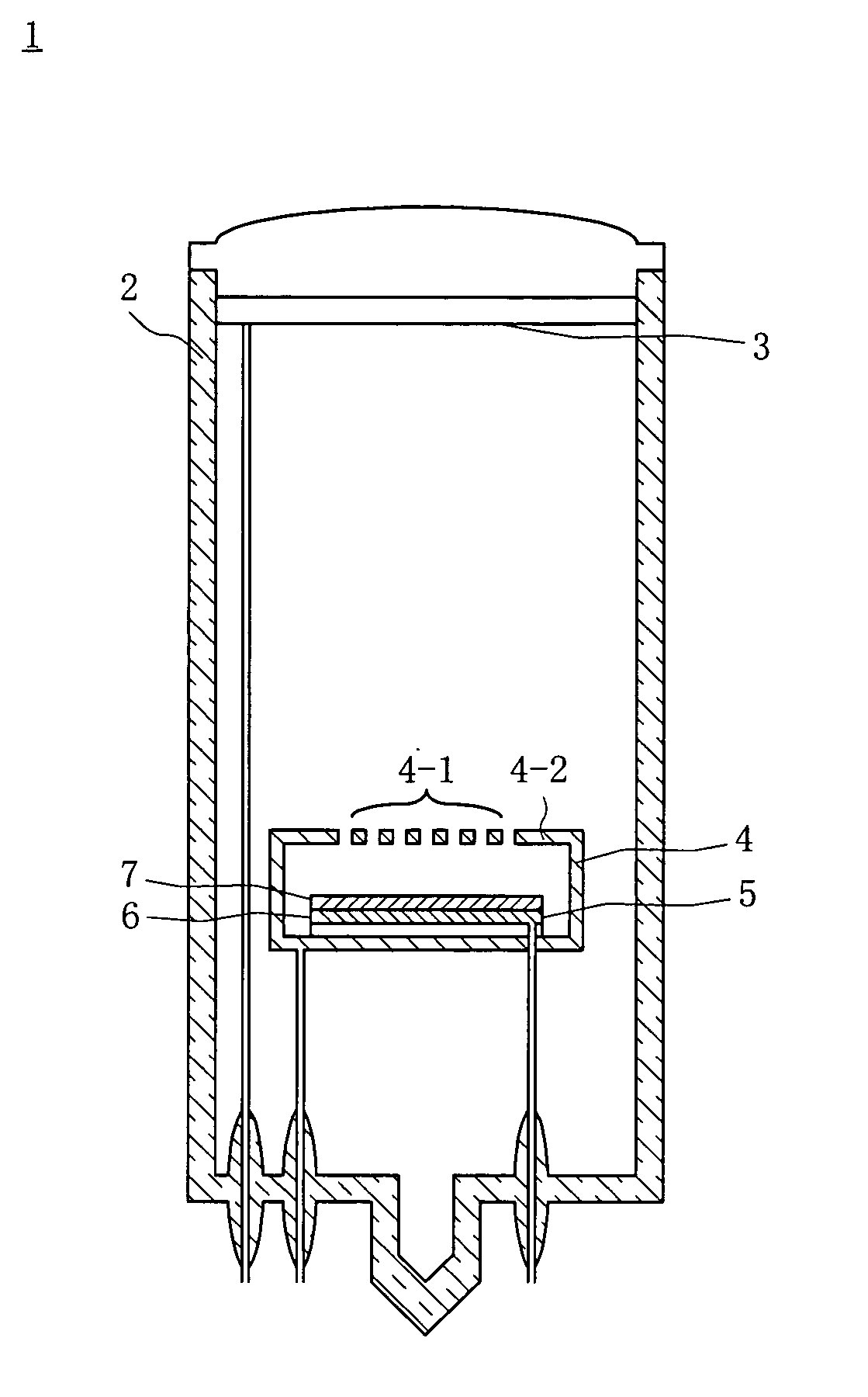
Figure 1 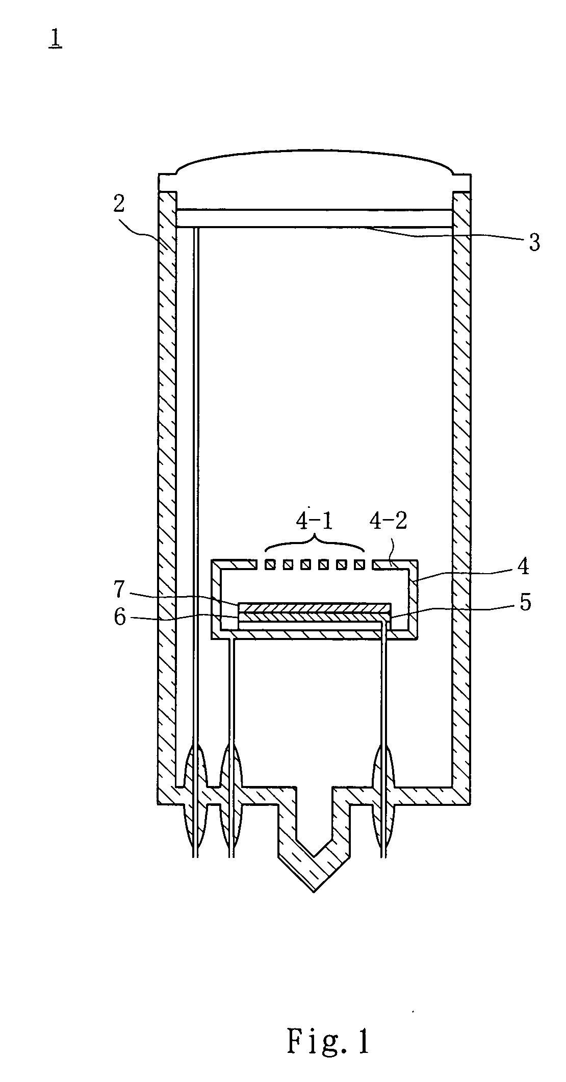
Figure 2 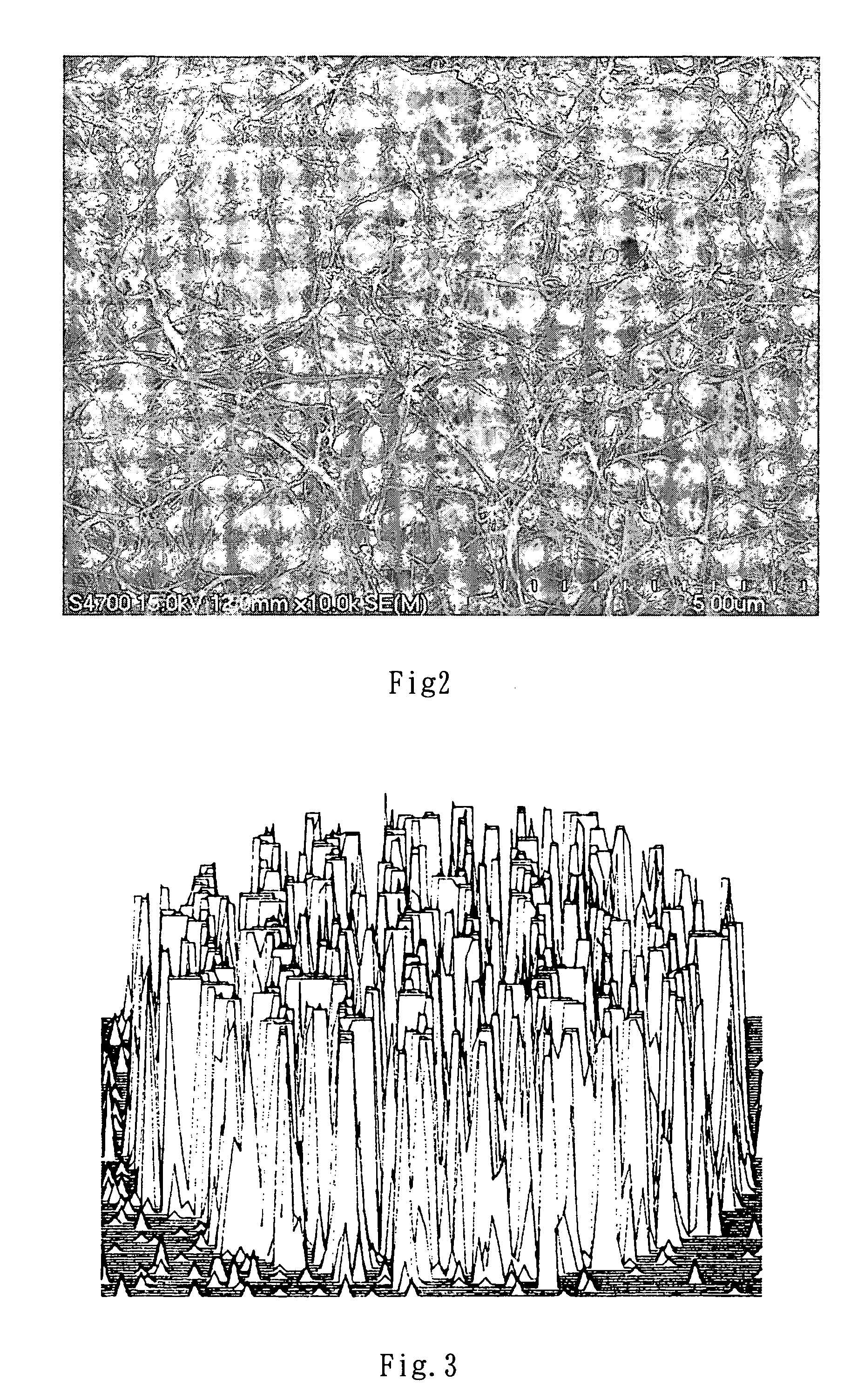
Figure 3
Abstract
Description
BACKGROUND OF THE INVENTION
[0001] The present invention relates to a method of manufacturing an electron-emitting source.
[0002] Conventionally, an FED (Field Emission Display) and vacuum fluorescent display use nanotube fibers such as CNTs (Carbon NanoTubes) or CNFs (Carbon NanoFibers) as an electron-emitting source. FIG. 8 shows such CNTs. As shown in FIG. 8, conventional CNTs are formed perpendicular to a cathode substrate (see Japanese Patent Laid-Open No. 11-329312).
[0003] According to another method, CNTs as described above are formed on a cathode substrate by printing. In this case, the substrate is irradiated with a CO2 laser or YAG laser to remove fillers and mixed fine graphite particles from the substrate surface, to expose the CNTs which form an electron-emitting source on the substrate surface (see Japanese Patent Laid-Open No. 2000-36243).
[0004] According to still another method, curled CNTs are formed on a cathode substrate by thermal CVD (see Japanese Patent Laid-...
Examples
Embodiment Construction
[0019] The embodiment of the present invention will be described in detail with reference to the accompanying drawings.
[0020] Referring to FIG. 1, a light source tube indicated by reference numeral 1 has a vacuum envelope 2 formed by fixing a transparent face glass plate to one end of a cylindrical glass tube by adhesion with low-melting frit glass, and welding, to the other end of the cylindrical glass tube, glass stems through which a plurality of lead pins are inserted and which are integrally formed with exhaust pipes. The interior of the vacuum envelope 2 is vacuum-evacuated to a pressure of about 10−3 Pa to 10−6 Pa.
[0021] In the vacuum envelope 2, an anode 3, on which phosphors (not shown) are deposited on its surface that opposes the face glass plate, is arranged on the end where the face glass plate is arranged. A substantially box-like gate structure 4 is formed to oppose the anode 3 such that a mesh portion 4-1 of the structure 4 faces the anode 3. A cathode structure 5 ...