
Multi port processor architecture
a processor and multi-port technology, applied in the direction of electric digital data processing, instruments, etc., can solve the problems of processor centric and unbalanced prior art systems, bus latency can be problematic, and latency can be even more problematic, so as to reduce memory access latency, avoid bus latencies, and reduce latency
Patent Information
- Authority / Receiving Office
- US · United States
- Patent Type
- Applications(United States)
- Current Assignee / Owner
- Publication Date
- 2006-05-11
- Estimated Expiration
- Not applicable · inactive patent
Smart Images

Figure 1 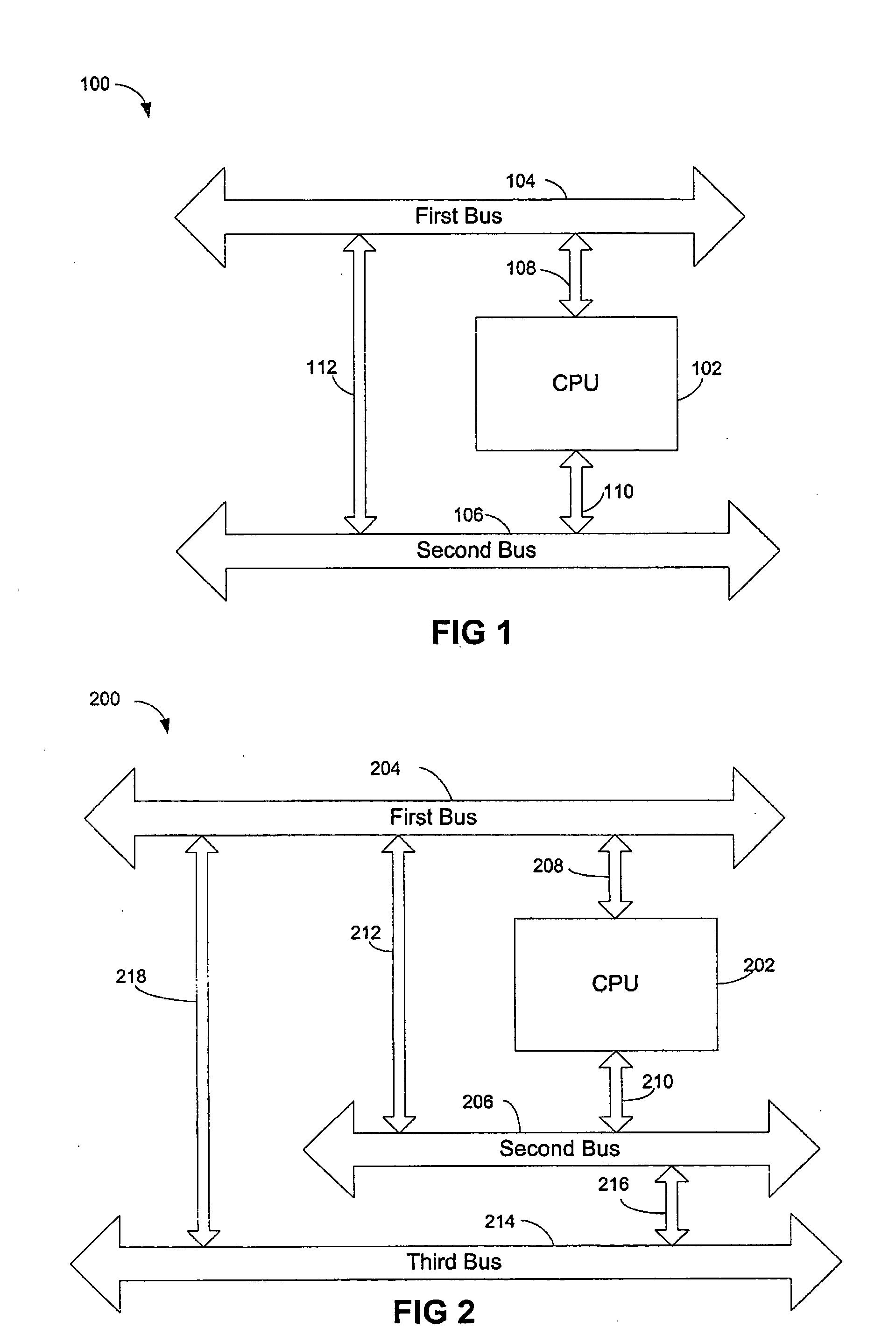
Figure 2 
Figure 3
Abstract
Description
BACKGROUND OF THE INVENTION
[0001] The present invention relates generally to computer bus architectures and to system-on-a-chip architectures with multi-port processors, including but not limited to embedded processors, application specific integrated circuits (ASICS), Field Programmable Arrays (FPGAs) and other programmable devices.
[0002] System-on-a-chip (SoC) design allows a designer to create complex silicon systems from smaller working blocks or systems. By providing a method for easily supporting proprietary functionality in a larger context that in a larger context that includes many existing design pieces, SoC design facilitates the use of silicon design for many systems. There are three views of traffic for a design which are important to differentiate, a memory centric view, a processor centric view and an input / output (I / O) view. Traditionally, prior art systems tend to be processor centric and not balanced. It is desirable that an SoC does not compromise one view over ...
Examples
Embodiment Construction
[0022] Throughout this description, the preferred embodiment and examples shown should be considered as exemplars, rather than limitations, of the present invention. The present invention, in accordance with various aspects, is directed to a multi-port processor architecture. The multi-port processor can be employed by system on a chip (SoC) designs to control the system aspects of the SoC.
[0023] Referring to FIG. 1, there is illustrated a system 100 in accordance with an aspect of the present invention. System 100 can be used for SoC designs. The system 100 comprises a CPU 102 that is coupled to a first bus 104 via a bi-directional interface 108. CPU 102 is also connected to a second bus 106 via bi-directional interface 110. A bi-directional interface 112, for example a bus bridge, is used to connect the first bus 104 to the second bus 106.
[0024] Optionally, bus 104 and / or bus 106 can be connected to a memory. For example, if a memory is coupled to the bus 104, then CPU 102 can u...