
Electro-optical device and electronic apparatus
a technology of optical devices and electronic devices, applied in semiconductor devices, semiconductor/solid-state device details, instruments, etc., can solve the problems of large leakage or flow of electromagnetic waves from electromagnetic shields
Patent Information
- Authority / Receiving Office
- US · United States
- Patent Type
- Applications(United States)
- Current Assignee / Owner
- Publication Date
- 2007-02-08
- Estimated Expiration
- Not applicable · inactive patent
Smart Images
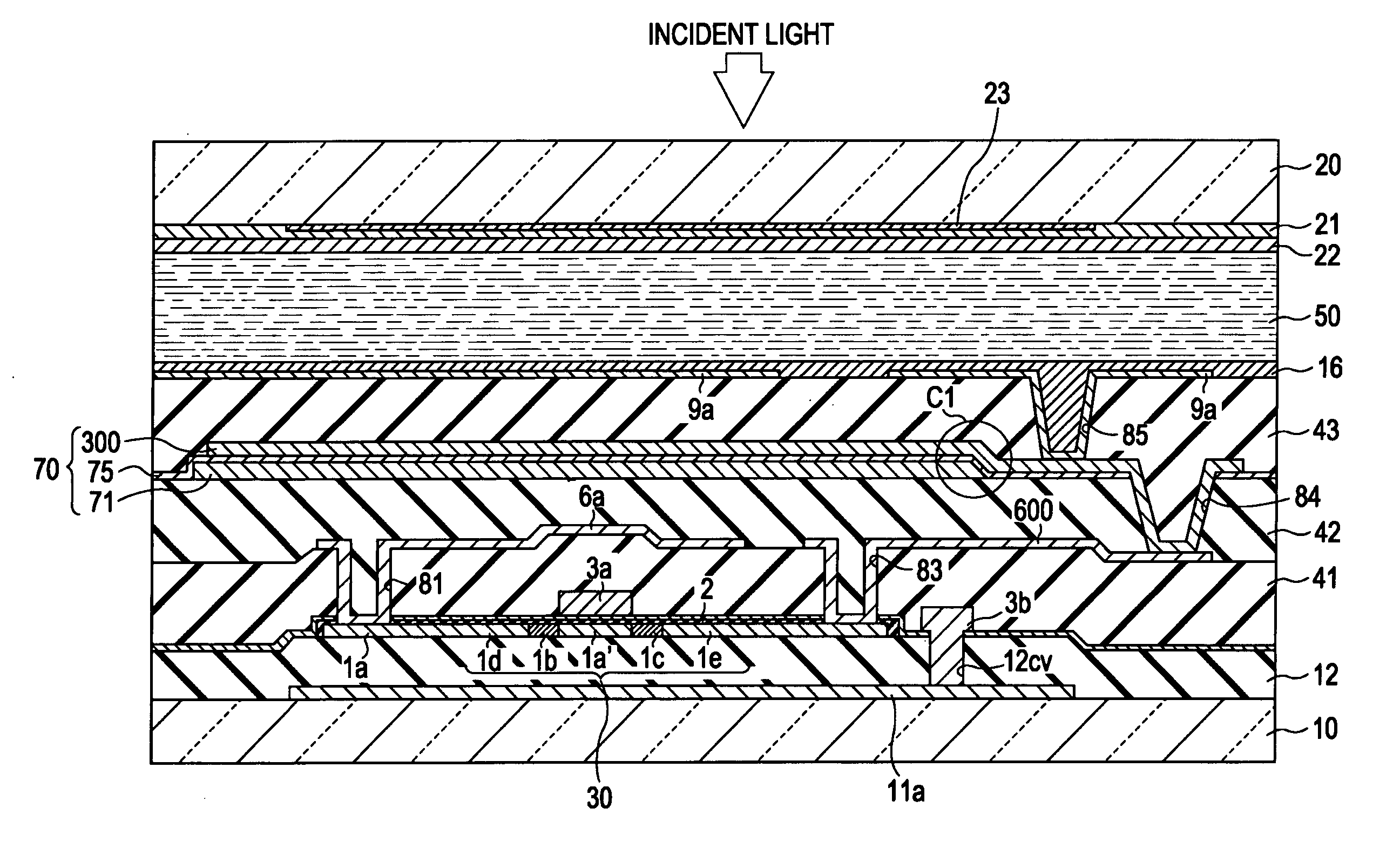
Figure 1 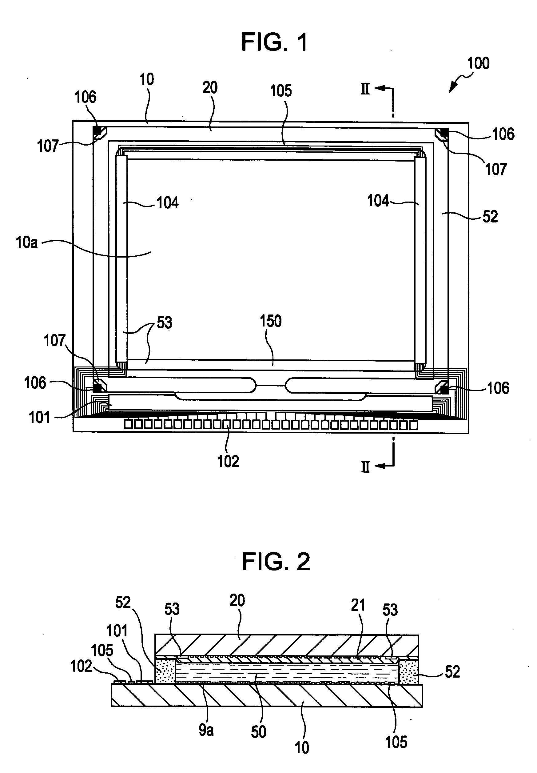
Figure 2 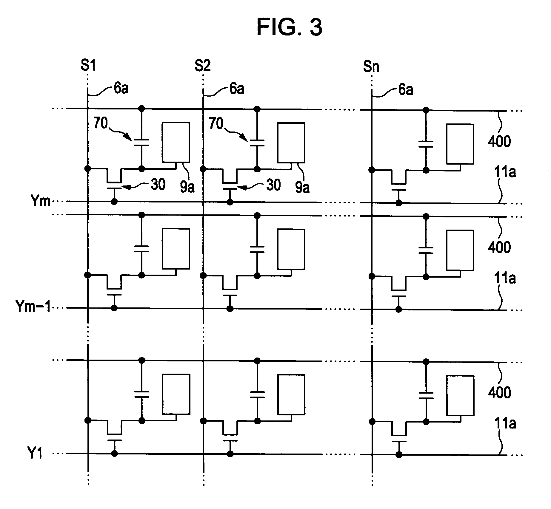
Figure 3
Abstract
Description
BACKGROUND
[0001] 1. Technical Field
[0002] The present invention relates to an electro-optical device which is suitable for high-definition image display, and to an electronic apparatus.
[0003] 2. Related Art
[0004] For example, electro-optical devices such as liquid crystal devices have a driving circuit having a data line driving circuit for driving data lines, a scanning line driving circuit for driving scanning lines, and a sampling circuit for sampling image signals. The driving circuit is provided onto a substrate constituting a display unit. In such a driving circuit, at a timing of a sampling circuit driving signal to be supplied from the data line driving circuit, the sampling circuit samples image signals to be supplied onto image signals and supplies the sampled image signals to the data lines.
[0005] In an electro-optical device, in order to suppress an increase of a driving frequency and achieve high-definition image display, serial image signals are converted into a p...
Examples
Embodiment Construction
[0044] Hereinafter, an embodiment of the invention will be described with reference to the drawings. FIG. 1 is a plan view showing the configuration of a liquid crystal panel. FIG. 2 is a cross-sectional view taken along the line II-II of FIG. 1. FIG. 3 is an equivalent circuit diagram of various elements, wiring lines, and so on in a plurality of pixels which are formed in a matrix shape so as to form an image display region of a liquid crystal panel. FIGS. 4 to 6 are plan views showing the partial configuration of a pixel portion on a TFT array substrate. FIGS. 4 and 5 correspond to a lower layer portion (FIG. 4) and an upper layer portion (FIG. 5) of a laminated structure described below. FIG. 6 is a plan view showing a laminated structure on a magnified scale, in which FIGS. 4 and 5 are superimposed. FIG. 7 is a cross-sectional view taken along the line VII-VII when FIGS. 4 and 5 are superimposed. FIG. 8 is a block diagram showing the configuration of a liquid crystal device. FI...