
Three terminal magnetic sensing devices having base lead layers in-plane with collector substrate materials and methods of making the same
a technology of base lead layer and collector substrate material, which is applied in the field of three-terminal magnetic sensors, can solve the problems of unnecessarily large track width, fragile and susceptible to damage of sensor stack structure, etc., and achieve the effect of increasing the number of areal recording
Patent Information
- Authority / Receiving Office
- US · United States
- Patent Type
- Applications(United States)
- Current Assignee / Owner
- Publication Date
- 2007-10-11
- Estimated Expiration
- Not applicable · inactive patent
Smart Images
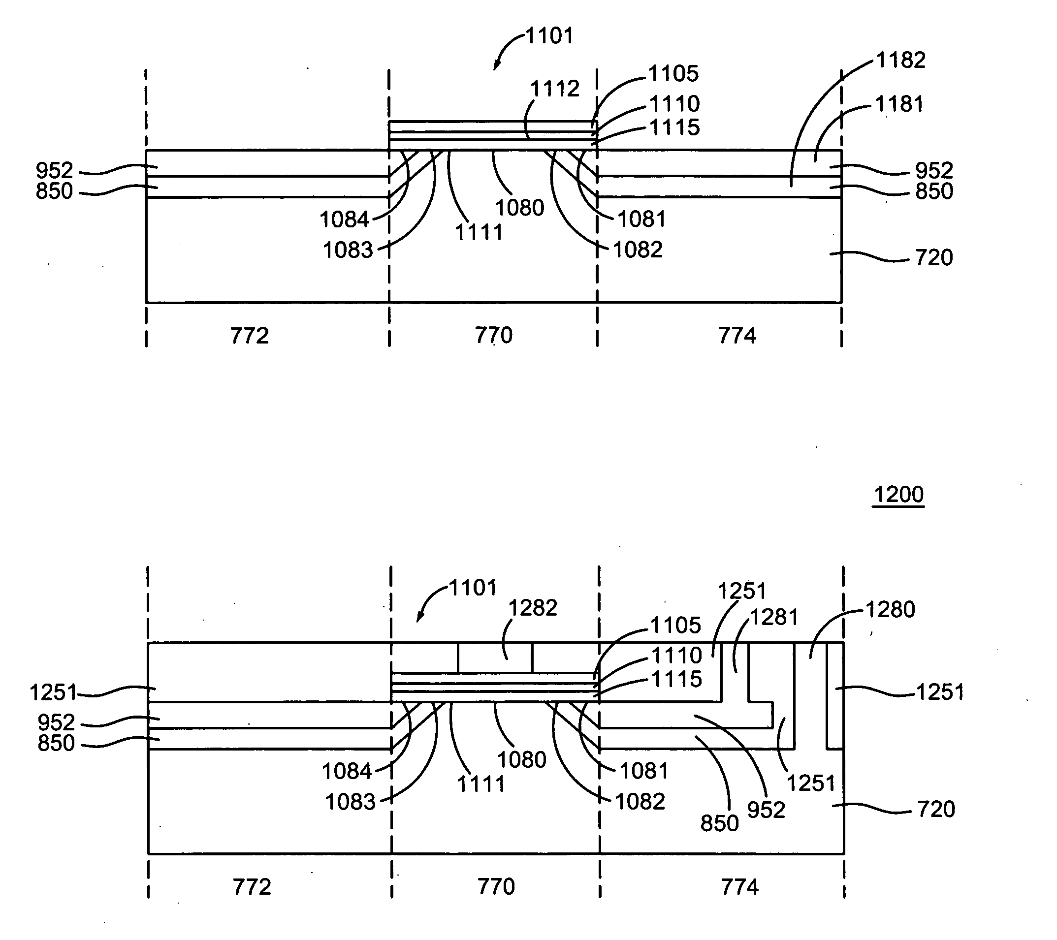
Figure 1 
Figure 2 
Figure 3
Abstract
Description
BACKGROUND
[0001] 1. Field of the Technology
[0002] The present application relates generally to three terminal magnetic sensors (TTMs) suitable for use in magnetic heads, and more specifically to TTMs having base lead layers in-plane with collector substrate materials.
[0003] 2. Description of the Related Art
[0004] Magnetoresistive (MR) sensors have typically been used as read sensors in hard disk drives. An MR sensor detects magnetic field signals through the resistance changes of a read element, fabricated of a magnetic material, as a function of the strength and direction of magnetic flux being sensed by the read element. The conventional MR sensor, such as that used as a MR read head for reading data in magnetic recording disk drives, operates on the basis of the anisotropic magnetoresistive (AMR) effect of the bulk magnetic material, which is typically permalloy. A component of the read element resistance varies as the square of the cosine of the angle between the magnetizati...
Examples
Embodiment Construction
[0028] Three terminal magnetic sensing devices (TTMs) having base lead layers in-plane with collector substrate materials, and methods of making the same, are disclosed. In one illustrative example, a collector substrate having an elevated region and a recessed region adjacent the elevated region is provided. An insulator layer is formed in full-film over the collector substrate, and a base lead layer is formed in full-film over the insulator layer and in-plane with semiconductor materials of the elevated region. The insulator materials and the base lead materials formed over the elevated region are then removed. Next, a sensor stack structure having an emitter region and a base region is formed over the elevated region such that part of the base region is formed over an end of the base lead layer. A base conductive via may be formed to contact base lead materials of the base lead layer at a suitable distance away from the sensor stack structure. Advantageously, the base conductive ...