
Jitter generating device and phase modulating device
a jitter generation and phase modulating technology, applied in the direction of demodulation, angle modulation, electric devices, etc., can solve the problems of increasing technical burden, requiring cost and space, and difficult to faithfully implement i(t) and q(t) signals, so as to achieve low cost and low cost. , the effect of low cos
Patent Information
- Authority / Receiving Office
- US · United States
- Patent Type
- Applications(United States)
- Current Assignee / Owner
- Publication Date
- 2008-04-17
- Estimated Expiration
- Not applicable · inactive patent
Smart Images
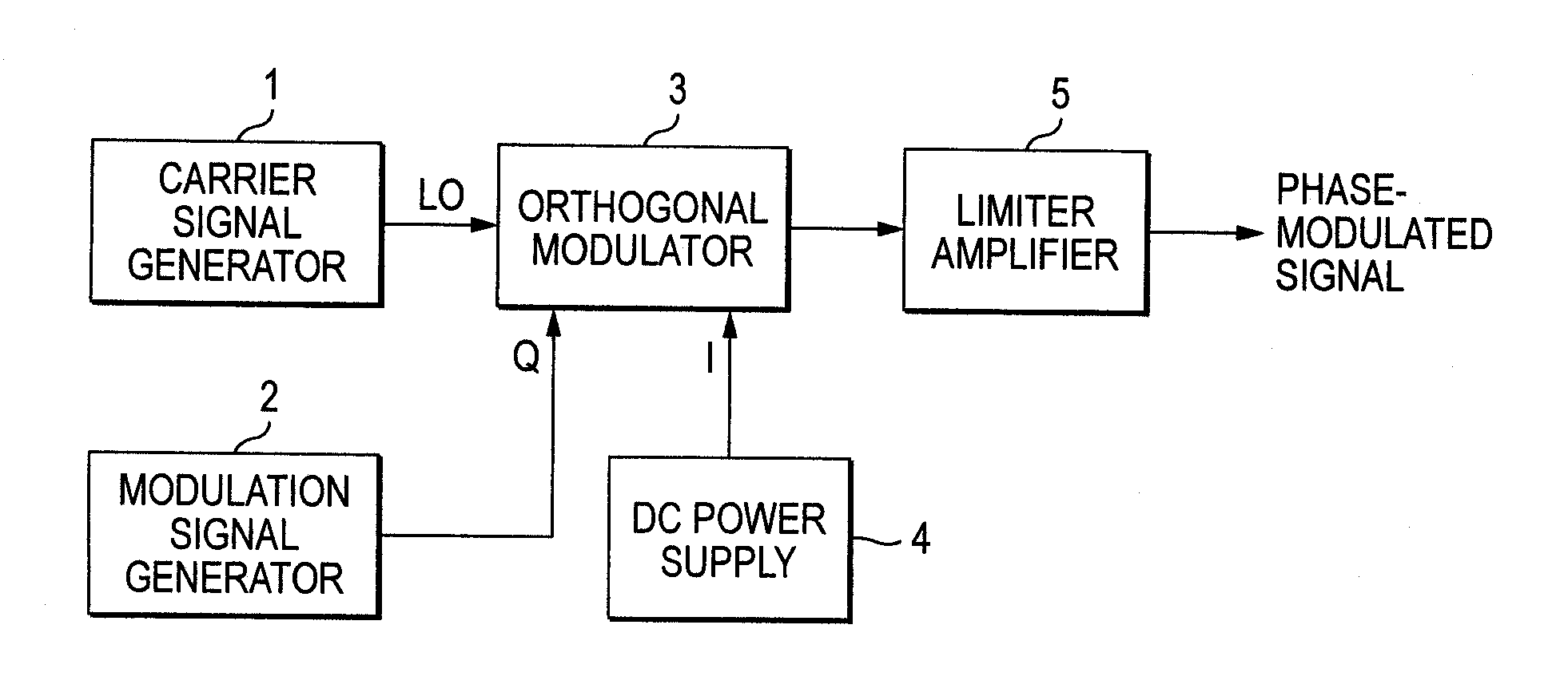
Figure 1 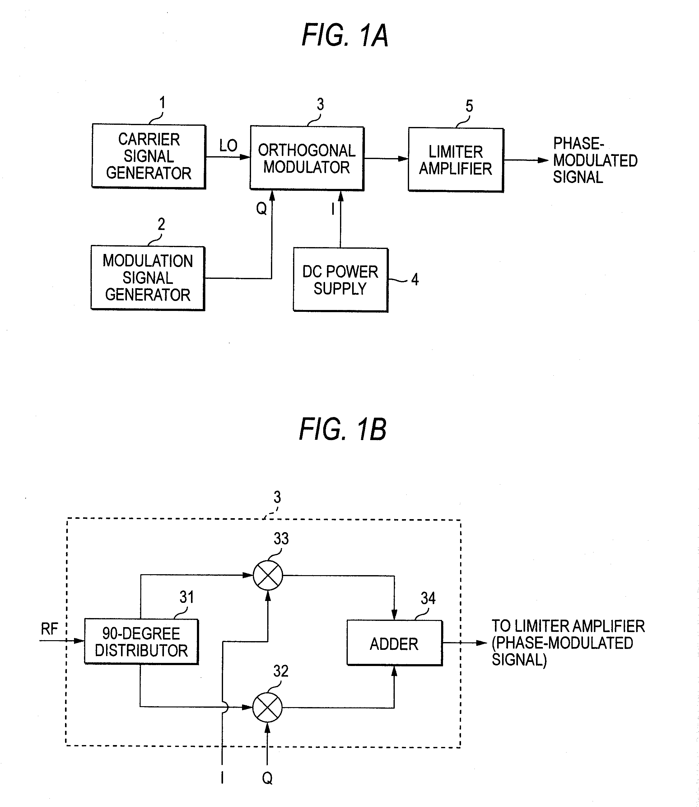
Figure 2 
Figure 3
Abstract
Description
[0001] This application is based on and claims priority from Japanese Patent Application No. 2006-277434, filed on Oct. 11, 2006, the entire contents of which are hereby incorporated by reference.BACKGROUND OF THE INVENTION
[0002] 1. Technical Field
[0003] The present disclosure relates to a jitter generating device for generating a jitter on a carrier signal and a phase modulating device for modulating a phase of the carrier signal, and more particularly to a jitter generating device and a phase modulating device which have a broad band.
[0004] 2. Related Art
[0005] For example, in a performance inspection of a communication device, a broadband jitter generating device has been required. For a related-art jitter generating device, as shown in FIG. 7A, there has been known a device that adds in an adder 23, a signal of a carrier signal generator 21 and that of a signal generator 22 having, as an oscillation frequency, a sum (ω+p) of a carrier signal frequency (ω) and a modulation signal freq...
Examples
Embodiment Construction
[0049]An exemplary embodiment of a phase modulating device according to the invention will be described below with reference to FIGS. 1 to 6.
[0050]FIG. 1A is a block diagram showing a structure according to an exemplary embodiment of the phase modulating device in accordance with the present invention.
[0051]As shown in FIG. 1A, a phase modulating device according to the exemplary embodiment includes: a carrier signal generator 1 for outputting a carrier signal having a frequency ω; a modulating signal generator 2 for outputting a modulation signal P=m·sin(pt); an orthogonal modulator 3; a DC power supply 4 for applying a DC voltage to the orthogonal modulator 3; and a limiter amplifier 5 (amplitude adjustment means) for amplifying a signal output from the orthogonal modulator 3 and adjusting an amplitude thereof to be constant.
[0052]As shown in FIG. 1A, the carrier signal transmitted from the carrier signal generator 1 is input to an LO input terminal of the orthogonal modulator 3. ...