

Semiconductor device and driving method thereof
a semiconductor device and driving method technology, applied in the field of semiconductor devices, can solve the problems of short data (information) holding period, increased cost per capacity, and difficulty in adequately reducing power consumption, and achieve the effect of sufficient reduction of power consumption of semiconductor devices, deterioration of elements, and extremely low frequency of refresh operations
Patent Information
- Authority / Receiving Office
- US · United States
- Patent Type
- Applications(United States)
- Current Assignee / Owner
- Publication Date
- 2011-07-21
Smart Images
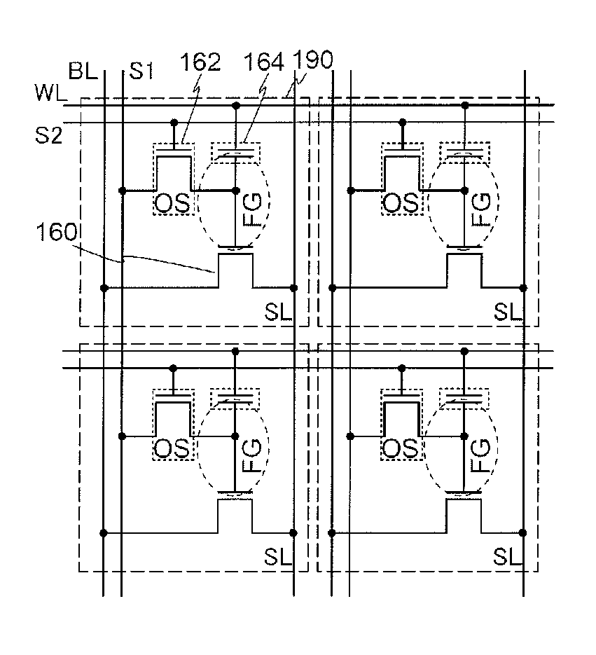
Figure 1 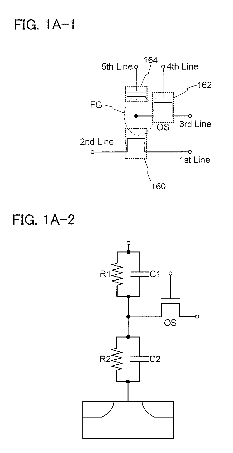
Figure 2 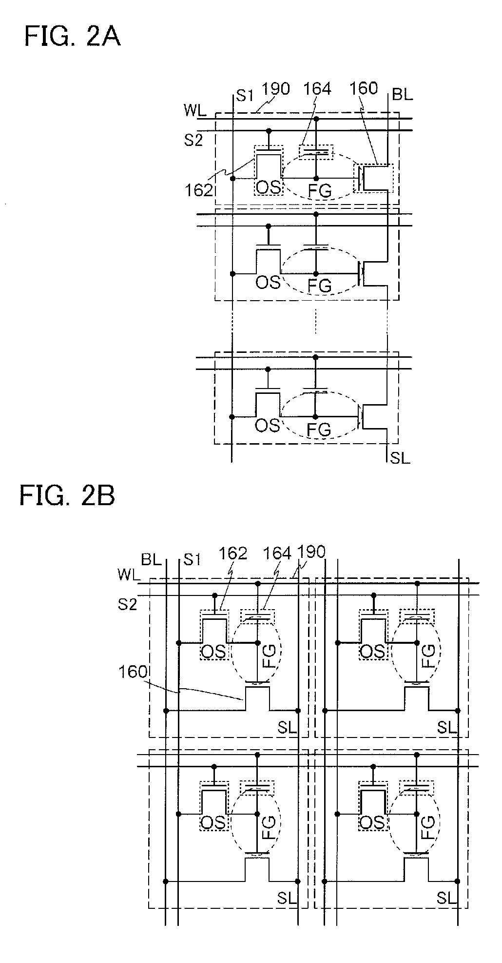
Figure 3
Abstract
Description
BACKGROUND OF THE INVENTION
[0001] 1. Field of the Invention
[0002] The disclosed invention relates to a semiconductor device using a semiconductor element and a manufacturing method thereof.
[0003] 2. Description of the Related Art
[0004] Memory devices using semiconductor elements are broadly classified into two categories: a volatile device that loses stored data when not powered, and a non-volatile device that holds stored data even when not powered.
[0005] A typical example of a volatile memory device is a dynamic random access memory (DRAM). A DRAM stores data in such a manner that a transistor included in a memory element is selected and charge is accumulated in a capacitor.
[0006] Owing to the above principle, charge in a capacitor is lost when data in a DRAM is read out thus, another writing operation is necessary every time data is read out. Moreover, since leakage current (off-state current) flows between a source and a drain of a transistor included in a memory element in an off sta...
Examples
embodiment 1
[0051]In this embodiment, a circuit structure and operation of a semiconductor device according to an embodiment of the disclosed invention will be described with reference to FIGS. 1A-1 and 1A-2. Note that in each of the circuit diagrams, “OS” may be written beside a transistor in order to indicate that the transistor includes an oxide semiconductor.
[0052]A semiconductor device in FIG. 1A-1 includes a non-volatile memory cell which includes a transistor 160, a transistor 162, and a capacitor 164. In FIG. 1A-1, one of a source electrode and drain electrode of the transistor 162, one electrode of the capacitor 164, and a gate electrode of the transistor 160 are electrically connected to one another. In addition, a first wiring (a 1st line, also referred to as a source line) and a source electrode of the transistor 160 are electrically connected to each other, and a second wiring (a 2nd line, also referred to as a bit line) and a drain electrode of the transistor 160 are electrically ...
embodiment 2
[0089]In this embodiment, an application example of the semiconductor device described in the above embodiment will be described with reference to FIGS. 2A and 2B and FIGS. 3A and 3B.
[0090]FIGS. 2A and 2B are circuit diagrams of semiconductor devices each including a plurality of semiconductor devices (hereinafter also referred to as memory cells 190) illustrated in FIG. 1A-1. FIG. 2A is a circuit diagram of a so-called NAND semiconductor device in which the memory cells 190 are connected in series, and FIG. 2B is a circuit diagram of a so-called NOR semiconductor device in which the memory cells 190 are connected in parallel.
[0091]The semiconductor device in FIG. 2A includes a source line SL, a bit line BL, a first signal line S1, a plurality of second signal lines S2, a plurality of word lines WL, and a plurality of memory cells 190. In FIG. 2A, one source line SL and one bit line BL are provided, but this embodiment is not limited to this. A plurality of source lines SL and a plu...
embodiment 3
[0107]In this embodiment, a structure and manufacturing method of a semiconductor device according to an embodiment of the disclosed invention will be described with reference to FIGS. 7A and 7B, FIGS. 8A to 8H, and FIGS. 9A to 9E.
[0108]FIGS. 7A and 7B illustrate an example of a structure of a semiconductor device. FIG. 7A illustrates a cross section of the semiconductor device, and FIG. 7B illustrates a plan view of the semiconductor device. Here, FIG. 7A illustrates a cross section taken along line A1-A2 and line B1-B2 in FIG. 7B. The semiconductor device illustrated in FIGS. 7A and 7B includes the transistor 160 including a semiconductor material which is not an oxide semiconductor in a lower portion, and the transistor 162 including an oxide semiconductor in an upper portion. The transistor 160 including a semiconductor material which is not an oxide semiconductor can operate at high speed easily. On the other hand, the transistor 162 including an oxide semiconductor can hold ch...