
Organic light emitting diode display device and method of manufacturing thereof
a light-emitting diode and display panel technology, applied in the field of display technology, can solve the problems of increased difficulty and cost of manufacturing process, poor user experience, etc., and achieve the effect of improving the alignment accuracy between the camera and the display panel
Patent Information
- Authority / Receiving Office
- US · United States
- Patent Type
- Applications(United States)
- Current Assignee / Owner
- Publication Date
- 2022-04-14
Smart Images
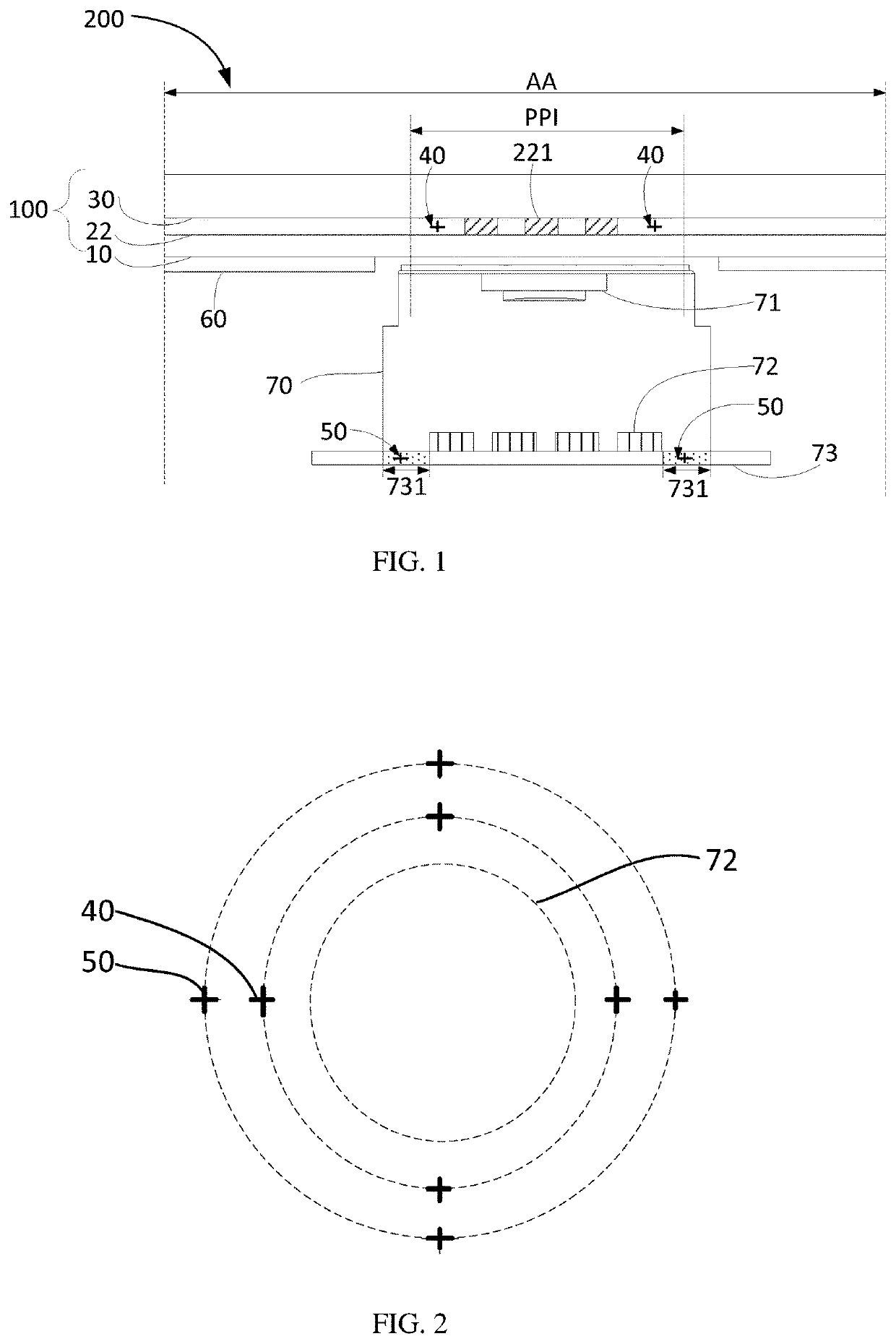
Figure 1 
Figure 2
Abstract
Description
[0001] The present application claims priority to Chinese Patent Application No. 201910821922.1, filed on Sep. 2, 2019, filed for the invention titled “Organic light emitting diode display device and method of manufacturing thereof,” which is hereby incorporated by reference in its entirety.BACKGROUND OF INVENTIONField of Invention
[0002] The present invention relates to the field of display technology, and more particularly, to an organic light emitting diode display device and a method of manufacturing thereof.Description of Prior Art
[0003] Active-matrix organic light emitting diode (AMOLED) full screens are relatively popular products. Enlarging a screen ratio may improve user experience. In order to achieve a high screen ratio, expanding a display area is achieved by adopting under-screen devices. Accordingly, all modules such as front camera, receiver, and fingerprint recognition of the mobile phone are disposed on a backside of the display screen.
[0004] In a currentl...
Examples
Embodiment Construction
[0034]In view of the technical problem of physical hollowing in the conventional display device, embodiments of the present invention may solve the problem.
[0035]Referring to FIG. 1, in one embodiment, an organic light emitting diode (OLED) display device 200 includes:
[0036]a display panel 100, and the display panel 100 is provided with a low pixel density area (PPI);
[0037]an attachment component 60 attached to a backside of the display panel 100, and an area of the attachment component corresponding to the low pixel density area is hollowed out; and
[0038]a camera 70 disposed on the backside of the display panel 100 and corresponding to the low pixel density area (PPI). A first alignment mark 40 is disposed in the low pixel density area (PPI) of the display panel 100, and a second alignment mark 50 is disposed inside the camera, and arrangements of the first alignment mark 40 and the second alignment mark 50 are consistent.
[0039]In one embodiment, the low pixel density area (PPI) ma...