
Multijunction solar cells
a solar cell and multi-junction technology, applied in the field of solar cells and the fabrication of solar cells, can solve the problems of affecting the performance of solar cells, the occurrence of anomalous events in photovoltaic arrays, and the difficulty of properly specifying and manufacturing
Patent Information
- Authority / Receiving Office
- US · United States
- Patent Type
- Applications(United States)
- Current Assignee / Owner
- Publication Date
- 2022-07-28
Smart Images
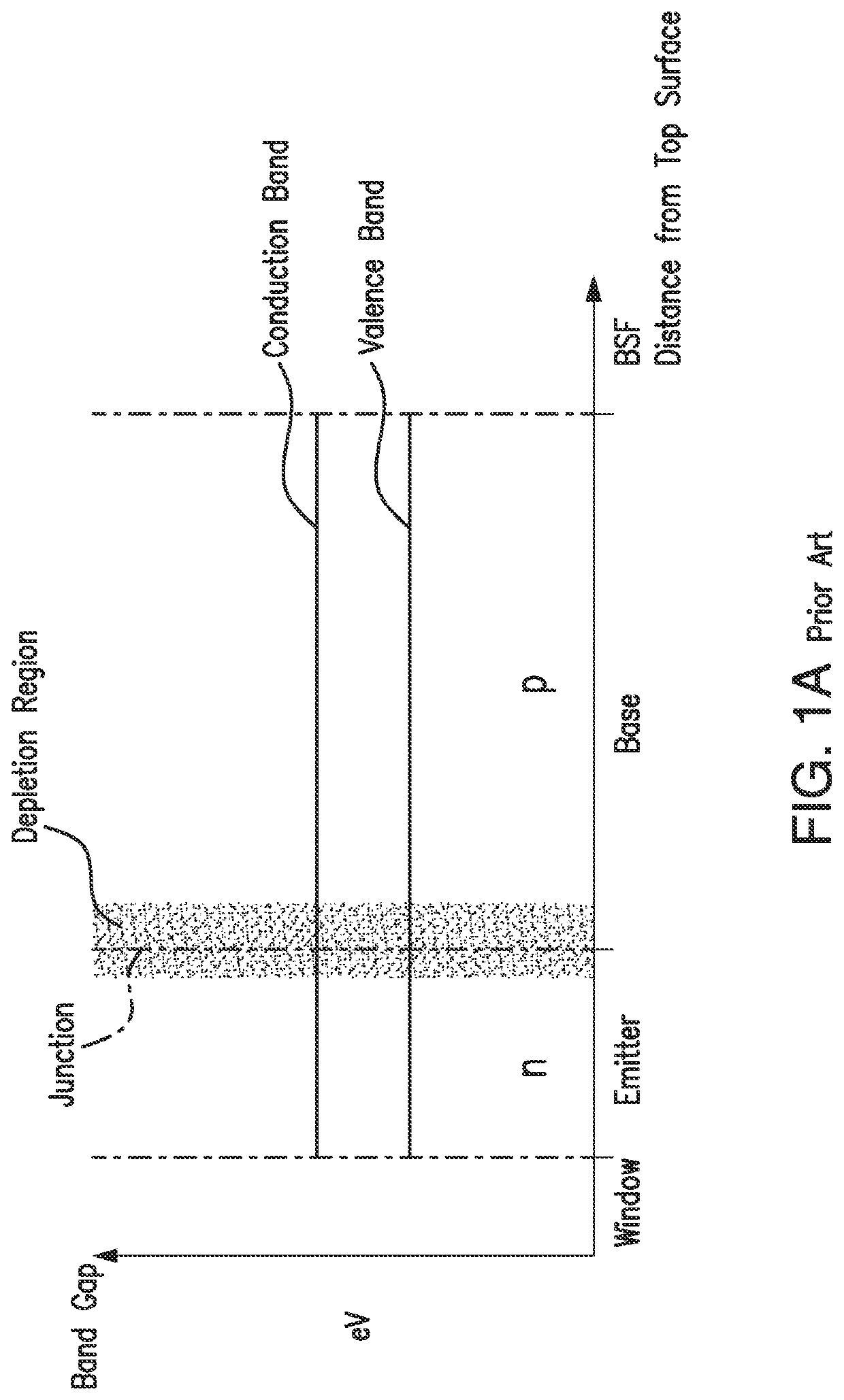
Figure 1 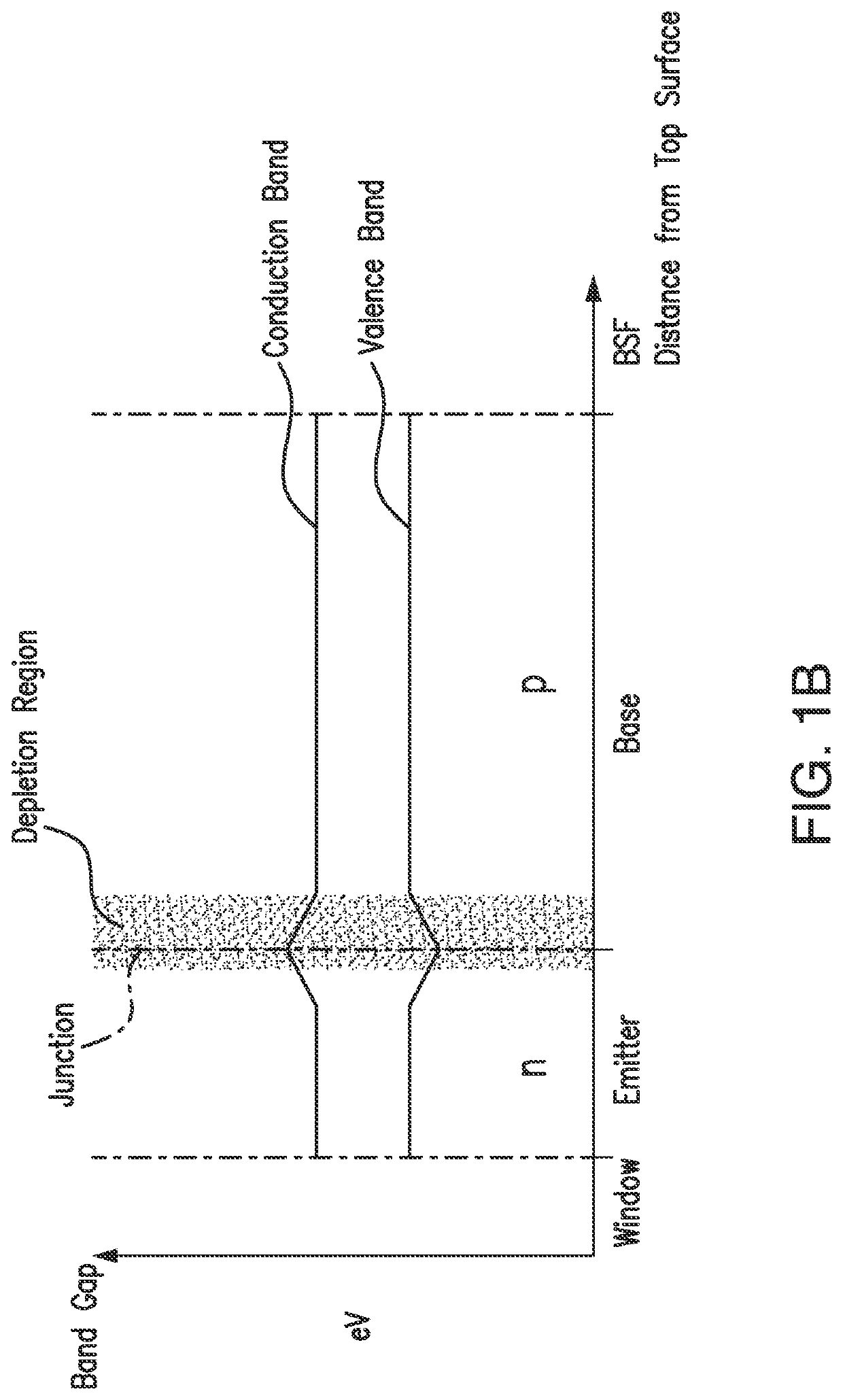
Figure 2 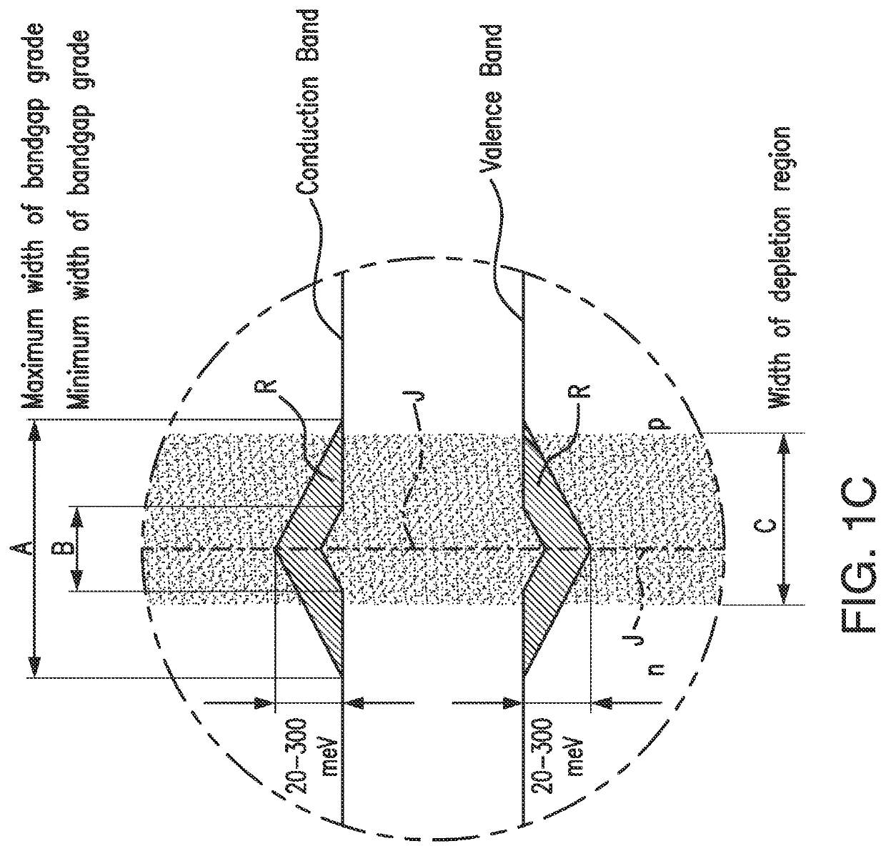
Figure 3
Abstract
Description
REFERENCE TO RELATED APPLICATIONS
[0001] This application is a divisional of U.S. patent application Ser. No. 17 / 161,314 filed Jan. 28, 2021.
[0002] The present application is related to U.S. patent application Ser. No. 15 / 681,144 filed Aug. 18, 2017, which is a continuation-in-part of Ser. No. 14 / 828,206 filed Aug. 17, 2015.
[0003] This application is related to U.S. patent application Ser. No. 14 / 660,092 filed Mar. 17, 2015, which is a division of U.S. patent application Ser. No. 12 / 716,814 filed Mar. 3, 2010, now U.S. Pat. No. 9,018,521; which is a continuation in part of U.S. patent application Ser. No. 12 / 337,043 filed Dec. 17, 2008.
[0004] This application is also related to U.S. patent application Ser. No. 16 / 667,687 filed Oct. 29, 2019 which is a division of Ser. No. 13 / 872,663 filed Apr. 29, 2012, now U.S. Pat. No. 10,541,349, which was also a continuation-in-part of application Ser. No. 12 / 337,043, filed Dec. 17, 2008.
[0005] This application is also related to U.S. patent applicati...
Examples
second embodiment
[0166]FIG. 1H is a and graph illustrating the band gap throughout the thickness of a solar subcell similar to that of FIG. 1B in a multijunction solar cell according to the present disclosure, in which the band gap is graded both in the emitter and base regions, in which in the emitter region it increases from the nominal band gap such as shown in FIG. 1A to a plateau at a higher band gap around the junction, and then decreases in the base region back down to the nominal band gap.
[0167]In some embodiments, the gradation in band gap increases to a certain level that is 20 meV to 300 meV greater than the nominal level, and then remains constant and plateaus at that level in the emitter region and continues at that level into the base regions symmetrically (or in other embodiments, non-symmetrically) around the junction. The gradation in band gap then decreases in the base region to the nominal band gap level as depicted in FIG. 1H.
third embodiment
[0168]FIG. 2A is an enlarged view of the band diagram around the junction and the depletion region of solar subcell similar to that of FIG. 1F depicting a graded band gap in that solar subcell according to the present disclosure in which the solar subcell is: (i) a homojunction; (ii) the band gap at the junction is greater than the band gap in both the n and p ungraded active region; (iii) the gradation in the band gap is symmetric around the junction with the width of the graded region in the n region being equal to the width of the graded region in the p region; (iv) the depletion region is asymmetric around the junction; (v) the width of the depletion region is shorter in the n region than in the p region; and (vi) the aggregate width of the depletion region is equal to the width of the region with a gradation in band gap.
[0169]Although the illustration in FIG. 2A is an embodiment with characteristics (i) through (vi) above, the present disclosure contemplates further variants of...
fourth embodiment
[0170]FIG. 2B is an enlarged view of the band diagram around the junction and the depletion region of solar subcell similar to that of FIG. 1F depicting a graded band gap in that solar subcell according to the present disclosure in which the solar subcell is: (i) a homojunction; (ii) the band gap at the junction is greater than the band gap in both the n and p ungraded active region; (iii) the gradation in the band gap is symmetric around the junction with the width of the graded region in the n region being equal to the width of the graded region in the p region; (iv) the depletion region is asymmetric around the junction; (v) the width of the depletion region is shorter in the n region than in the p region; and (vi) the aggregate width of the depletion region is equal to the width of the region with a gradation in band gap.
[0171]Although the illustration in FIG. 2B is an embodiment with characteristics (i) through (vi) above, the present disclosure contemplates further variants of...