
Method for creating waveguides in multilayer ceramic structures and a waveguide having a core bounded by air channels
a multi-layer ceramic and waveguide technology, applied in waveguides, electrical equipment, antennas, etc., can solve the problems of large physical size compared to the rest of the circuit unit to be manufactured, increased cost and failure risk, and difficult integration of their manufacture into the manufacturing of the circuit unit as a whol
Patent Information
- Authority / Receiving Office
- US · United States
- Patent Type
- Patents(United States)
- Current Assignee / Owner
- Publication Date
- 2005-06-21
- Estimated Expiration
- Not applicable · inactive patent
Smart Images
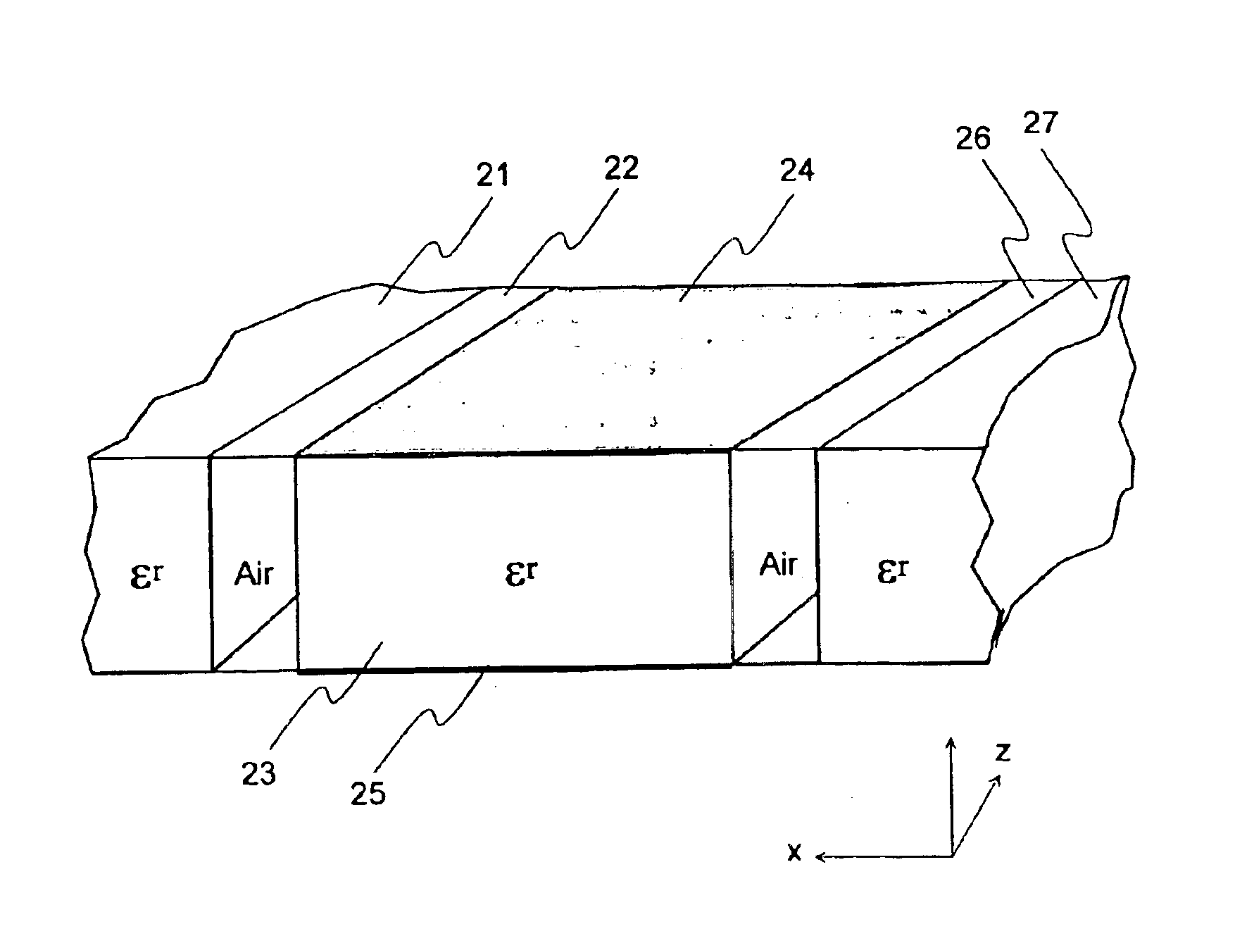
Figure 1 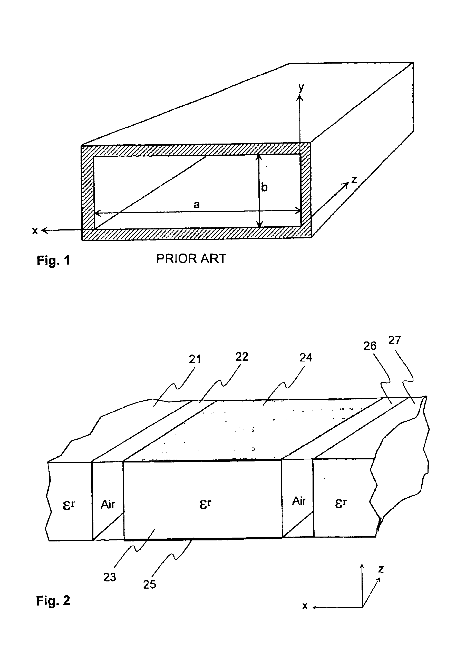
Figure 2 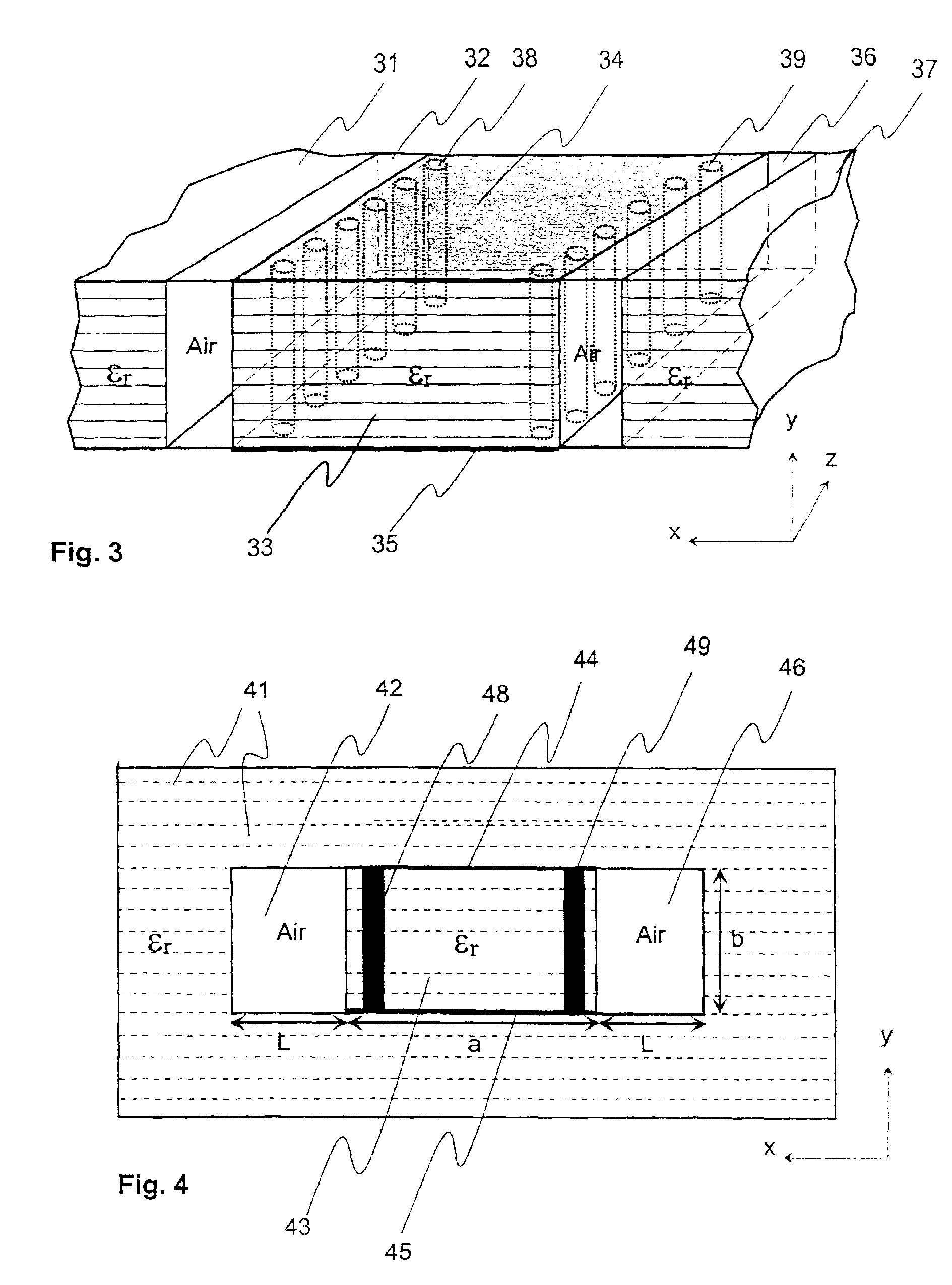
Figure 3
Abstract
Description
PRIORITY CLAIM
[0001] This is a national stage of PCT application No. PCT / FI00 / 00635, filed on Jul. 10, 2000. Priority is claimed on that application, and on patent application No. 991585 filed in Finland on Jul. 9, 1999.FIELD OF THE INVENTION
[0002] The invention relates to a method for creating waveguides in circuit board units manufactured with the multilayer ceramic technique, in which method the dimensions and structural directions of the circuit board units can be defined by means of x, y and z axes perpendicular to each other, and the circuit board unit is assembled of separate ceramic layers, the permittivity εr of which is higher than the corresponding value of air, and in which layers cavities and holes of the desired shape can be made, and on the surface of which ceramic layer a conductive material can be printed at the desired location by silk screen printing, and the circuit board unit is completed by exposing the unit to a high temperature.
[0003] The invention also relates ...
Examples
first embodiment
[0032]FIG. 2 shows an example of a waveguide according to the invention, implemented with the multilayer ceramic technique. The structure shown in FIG. 2 is part of a larger circuit structure implemented with the multilayer ceramic technique, which is not shown in its entirety in the drawing. The waveguide structure is surrounded on both sides by the structures 21 and 27 shown in the drawing, which consist of several green tapes. The permittivity εr of the ceramic material used in them is clearly higher than the permittivity of air, which is of the magnitude 1, as is well known. Other parts of the structure, which are both above and below the waveguide structure shown in the drawing, viewed in the direction of the y-axis, consist mainly of the same ceramic material. The core part 23 of the waveguide consists of the same ceramic material as the rest of the circuit structure. The width of the waveguide in the direction of the x-axis is limited by air-filled cavities 22 and 26 essentia...
second embodiment
[0034]FIG. 3 shows an example of a waveguide according to the invention. The structure shown in FIG. 3 is part of a larger structure implemented with the multilayer ceramic technique, which is not shown in its entirety in the drawing. The waveguide structure is surrounded on both sides by the structures 31 and 37 shown in the drawing, which consist of several green tapes. The permittivity εr of the ceramic material used in them is clearly higher than the permittivity of air, which is of the magnitude 1. Other parts of the structure, which are both above and below the waveguide structure shown in the drawing, viewed in the direction of the y-axis of the drawing, also consist mainly of the same ceramic material. The core part 33 of the waveguide consists of the same ceramic material as the rest of the circuit structure. The width of the waveguide in the direction of the x-axis is limited by two essentially parallel impedance discontinuities, which are formed of via posts 38 and 39 in ...