
Counting circuit of semiconductor device and duty correction circuit of semiconductor device using the same
a duty correction circuit and semiconductor technology, applied in the field of semiconductor devices, can solve the problems of short lock time, binary search method disadvantage, linear search method disadvantage, etc., and achieve the effect of minimizing the probability of an error occurring during an operation
Patent Information
- Authority / Receiving Office
- US · United States
- Patent Type
- Patents(United States)
- Current Assignee / Owner
- Publication Date
- 2014-01-07
Smart Images
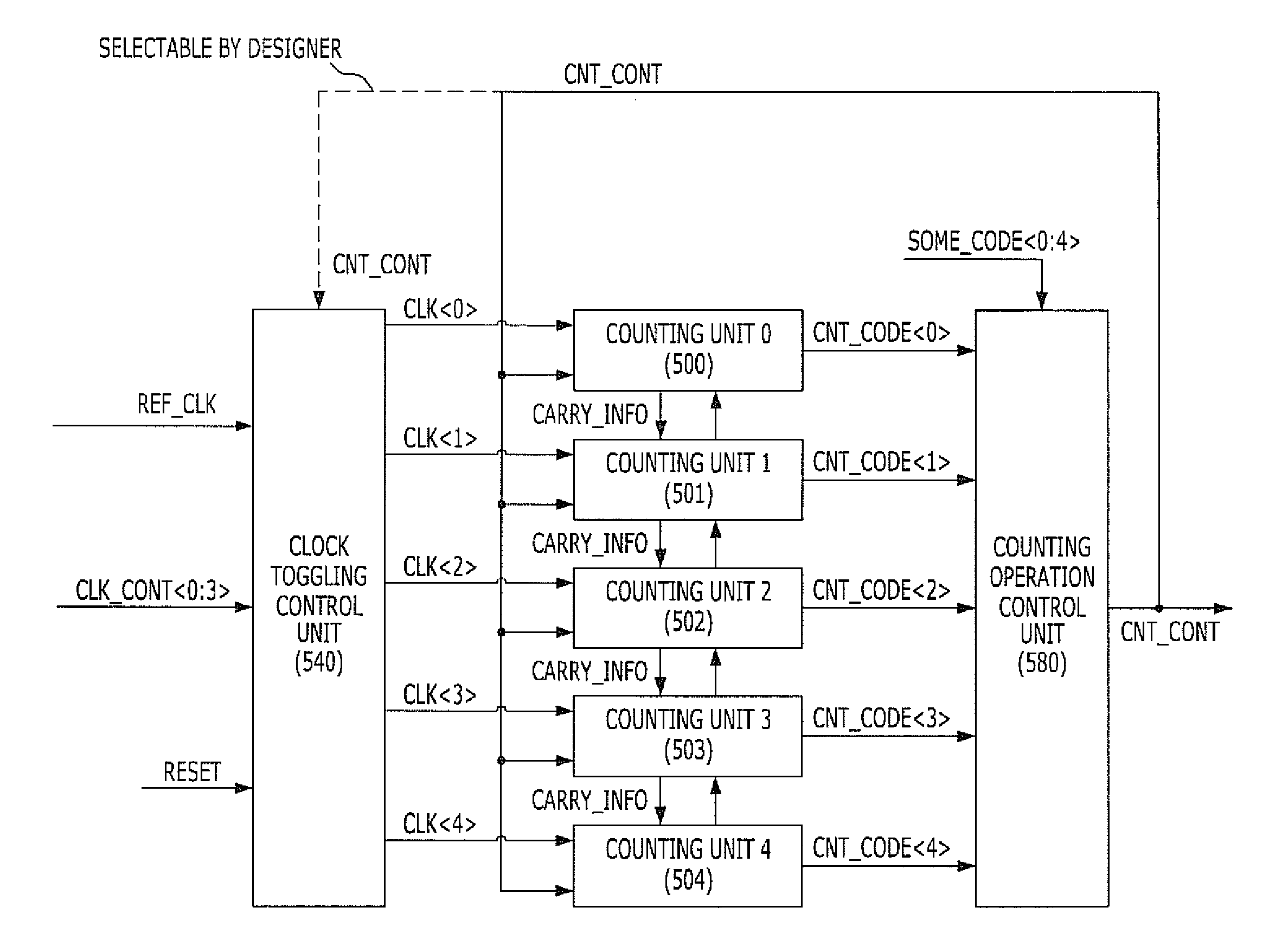
Figure 1 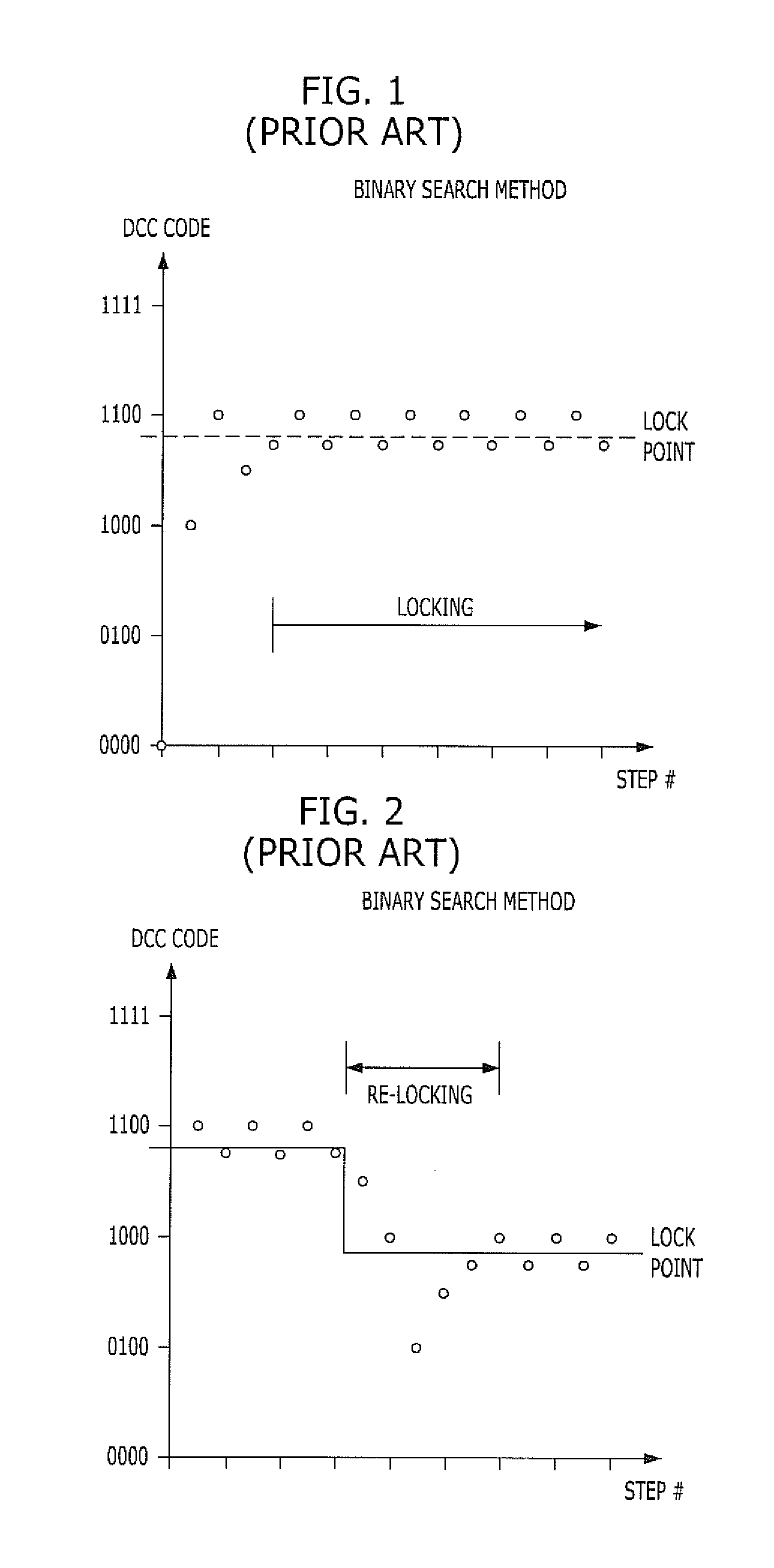
Figure 2 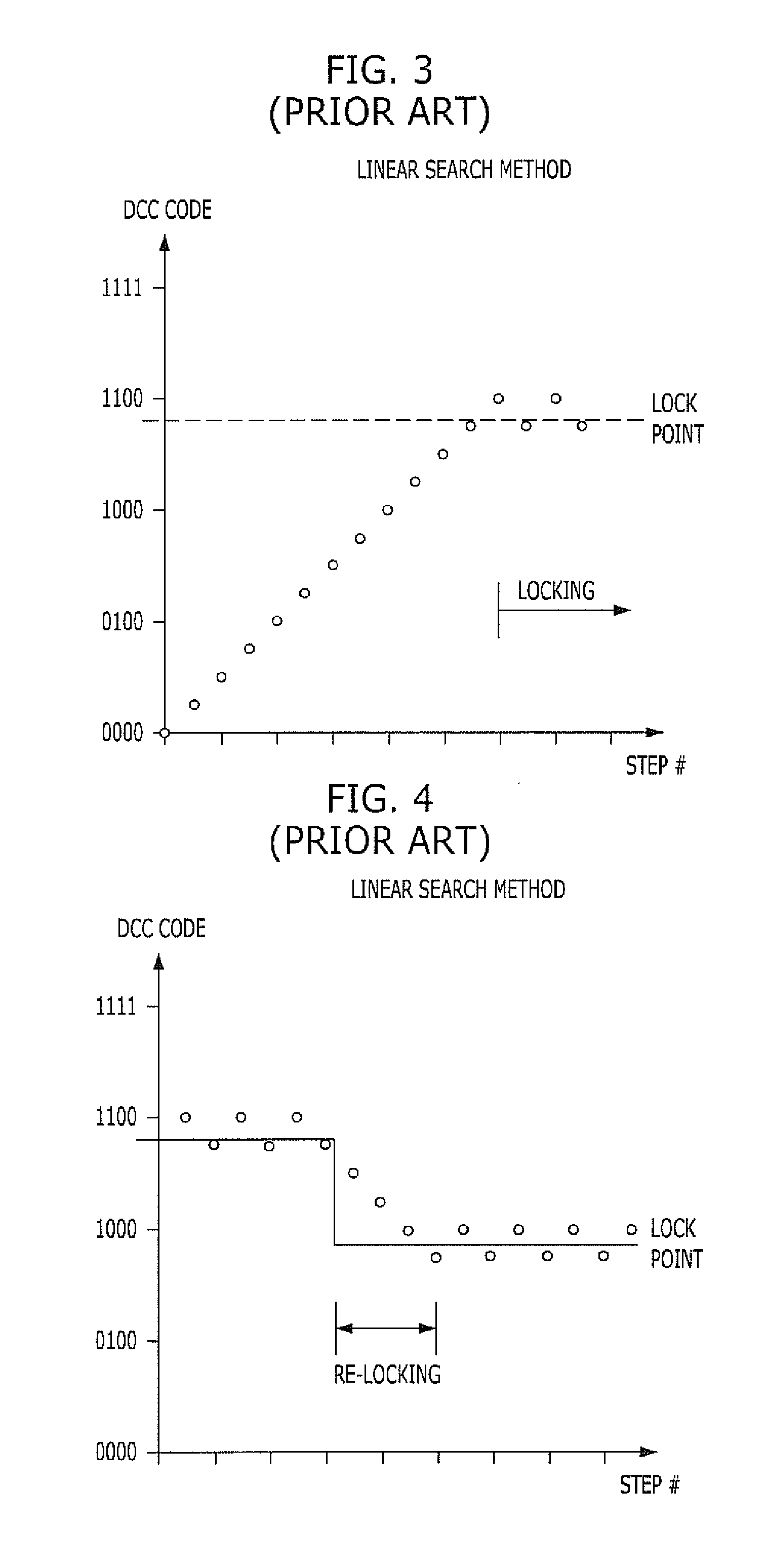
Figure 3
Abstract
Description
CROSS-REFERENCE TO RELATED APPLICATIONS
[0001] The present application claims priority of Korean Patent Application No. 10-2011-0077463, filed on Aug. 3, 2011, which is incorporated herein by reference in its entirety.BACKGROUND
[0002] 1. Field
[0003] Exemplary embodiments of the present invention relate to semiconductor devices, and more particularly, to a counting circuit of a semiconductor device and a duty correction circuit of a semiconductor device that are implemented to the counting circuit of a semiconductor device.
[0004] 2. Description of the Related Art
[0005] The duty cycle of a clock is the ratio of the duration that an input clock is at a high logic level, or a low logic level, to the total period of the input clock signal. A circuit for detecting the duty cycle of an input clock generates a value indicating that the duty of a period is larger or smaller than 50%, and a duty correction circuit performs an operation to correct the duty cycle of the input clock by using the value...
Examples
first embodiment
[0034]The detailed configuration of the clock toggling control unit 540 will be described below with reference to FIG. 6. The clock toggling control unit 540 includes a toggling operation control signal generation part 542 configured to generate a plurality of toggling operation control signals TOGGL_CONT. The clock toggling control unit 540 also includes a plurality of counting clock generation parts 544 configured to generate the counting clocks CLK in response to the respective toggling operation control signals TOGGL_CONT and the source clock REF_CLK. The toggling operation control signals TOGGL_CONT are sequentially activated from a deactivated signal each time the source clock REF_CLK toggles during the period when the counting control signal CNT_CONT is deactivated. Also, the toggling operation control signals TOGGL_CONT are all activated, or determined not to be active, during the period when the counting control signal CNT_CONT is activated in the initial operations of the...
second embodiment
[0043]The detailed configuration of the clock toggling control unit 540 will be described below with reference to FIG. 6. The clock toggling control unit 540 includes a toggling operation control signal generation part 542 configured to generate a plurality of toggling operation control signals TOGGL_CONT. The clock toggling control unit 540 also includes a plurality of counting clock generation parts 544 configured to generate the counting clocks CLK in response to the respective toggling operation control signals TOGGL_CONT and the source clock REF_CLK. The toggling operation control signals TOGGL_CONT are sequentially activated each time a source clock REF_CLK toggles. All of the toggling operation control signals TOGGL_CONT are activated, or determined not to be activated, when the number of activated signals is equal to or greater than the designated number.
[0044]The toggling operation control signal generation part 542 includes an initialization determining section 5422 and a...