
Semiconductor device having a transparent window for passing radiation
a technology of semiconductor devices and radiation, applied in the direction of radiation controlled devices, semiconductor devices, electrical equipment, etc., can solve the problems of subjecting the die and wire bonds of the package to the harsh molding environment, and affecting the cost of the final product, so as to achieve convenient and reliable
Patent Information
- Authority / Receiving Office
- US · United States
- Patent Type
- Patents(United States)
- Current Assignee / Owner
- Publication Date
- 2017-04-11
Smart Images
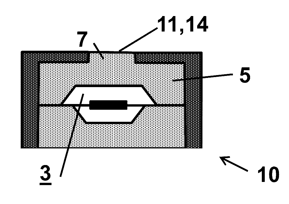
Figure 1 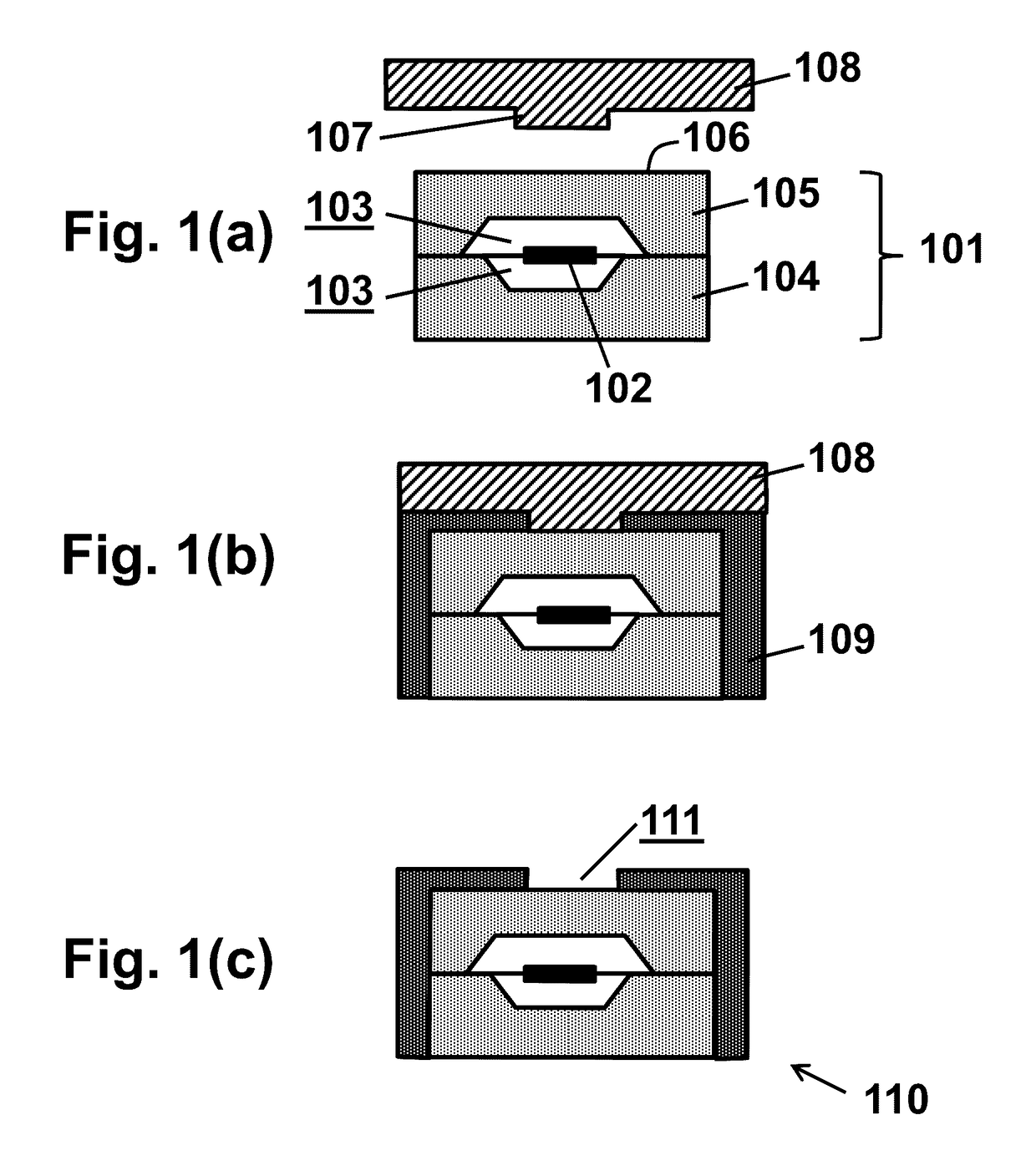
Figure 2 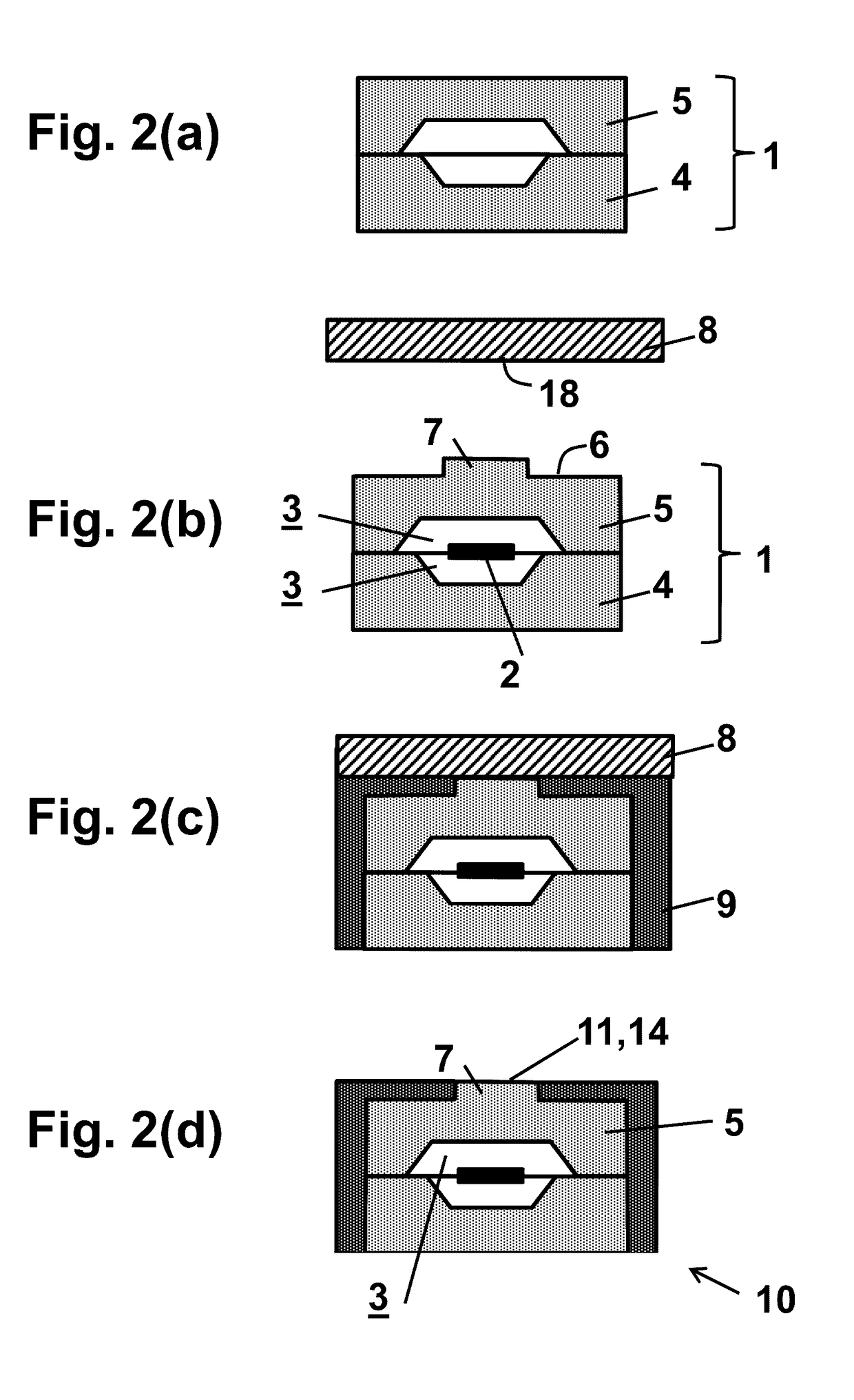
Figure 3
Abstract
Description
FIELD OF THE INVENTION
[0001] The present invention relates to the field of methods of manufacturing semiconductor devices and to semiconductor devices thus obtained, more in particular to methods of packaging semiconductor devices such as e.g. IR-sensors, in a package having a transparent window for passing radiation, e.g. IR-light, and to devices obtained by such methods.BACKGROUND OF THE INVENTION
[0002] Several packages and packaging techniques for encapsulating integrated circuits are known in the art, such as glass, metal, ceramic and plastic packages.
[0003] As electronic products increase in functionality and complexity, there is an emphasis on affordability, miniaturization, and energy efficiency of the semiconductor devices as a whole. The telecommunications, automotive, and commercial electronic markets are the leading drivers for these trends. These markets see high volume manufacturing with millions of units on a yearly basis. The choice of the packaging material for the elec...
Examples
Embodiment Construction
[0052]The present invention will be described with respect to particular embodiments and with reference to certain drawings but the invention is not limited thereto but only by the claims. The drawings described are only schematic and are non-limiting. In the drawings, the size of some of the elements may be exaggerated and not drawn on scale for illustrative purposes. The dimensions and the relative dimensions do not correspond to actual reductions to practice of the invention.
[0053]The terms first, second and the like in the description and in the claims, are used for distinguishing between similar elements and not necessarily for describing a sequence, either temporally, spatially, in ranking or in any other manner. It is to be understood that the terms so used are interchangeable under appropriate circumstances and that the embodiments of the invention described herein are capable of operation in other sequences than described or illustrated herein.
[0054]Moreover, the terms top,...