
Semiconductor light emitting diode chip with current extension layer and graphical current extension layers
a technology of light-emitting diodes and semiconductors, applied in the direction of semiconductor devices, basic electric elements, electrical apparatus, etc., can solve the problems of reducing the reliability of the chip, the area of the light-emitting compound is increased, and the nitride semiconductor used to generate the epitaxial layer is not a perfect crystal, etc., to achieve the effect of increasing the area of the light-emitting compound, increasing the adhesion of the pad on the surfa
Patent Information
- Authority / Receiving Office
- US · United States
- Patent Type
- Patents(United States)
- Current Assignee / Owner
- Publication Date
- 2017-05-30
Smart Images
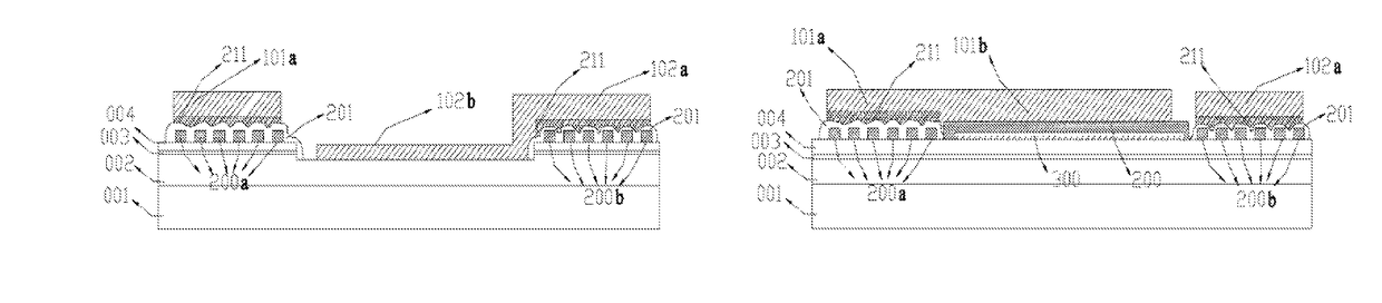
Figure 1 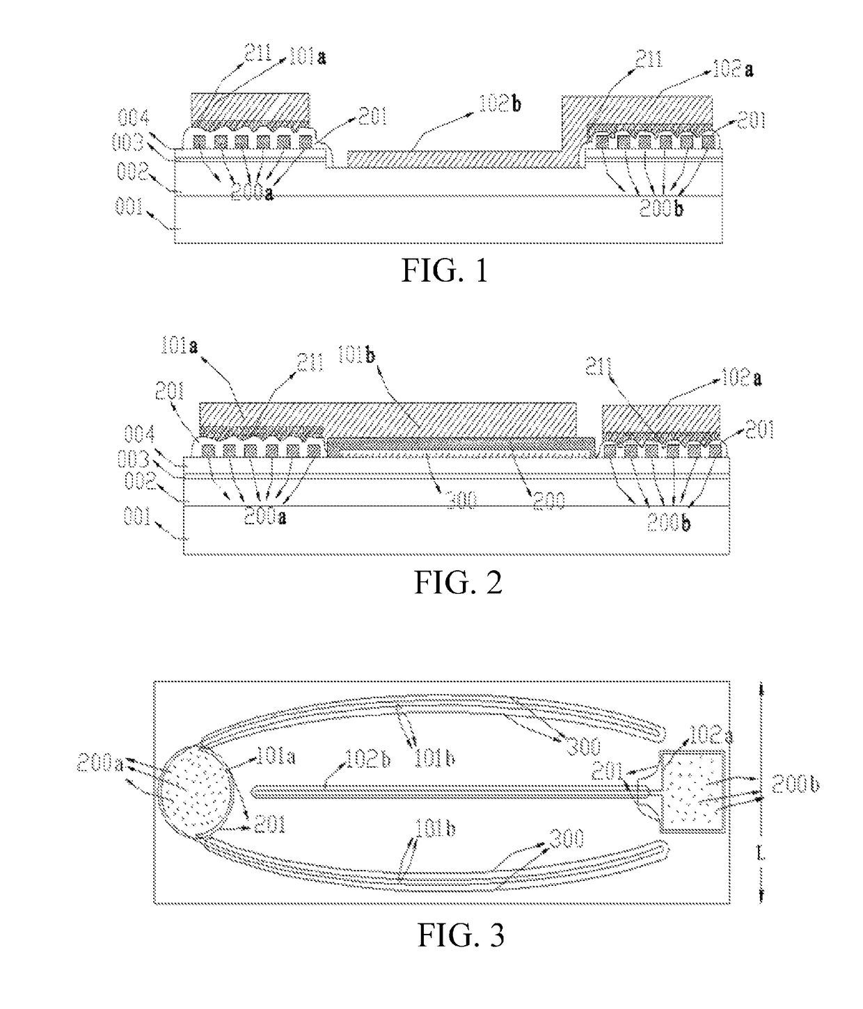
Figure 2
Abstract
Description
CROSS-REFERENCE TO RELATED APPLICATIONS
[0001] This application is the United States national phase of International Application No. PCT / CN2014 / 073361, filed Mar. 13, 2014, and claims priority to Chinese Application Nos. 201310598862.4 and 201320747631.0, both filed Nov. 25, 2013, the disclosures of which are hereby incorporated in their entirety by reference.BACKGROUND
[0002] Technical Field
[0003] The present invention relates to the field of production technologies of a light emitting diode, and in particular, to production technologies of a light emitting diode chip.
[0004] Related Art
[0005] With the advancement of epitaxial technologies, brightness of a semiconductor light emitting diode is improved year by year. According to power, a chip may be divided into a large-power chip, a medium-power chip, and a small-power chip. Large power means a large-size chip. However, 5 years before, large-size and large-power brightness now has been replaced with the medium-size chip, which has lower c...
Examples
Embodiment Construction
[0021]As shown in FIGS. 1, 2, and 3: An N-type semiconductor layer 002, a light emitting compound layer 003, and a P-type semiconductor layer 004, and an N-type semiconductor layer 002 that is exposed in the middle of the P-type semiconductor layer 004 after being etched are sequentially disposed on a rectangular substrate 001 having a narrow side L (which is as shown in FIG. 3) less than 300 um. P-type semiconductor layers 004 on two sides of the rectangular substrate 001 are respectively provided with a P pad 101a and an N pad 102a.
[0022]P-type semiconductor layers 004 corresponding to the P pad 101a and the N pad 102a are respectively provided with graphical current extension layers 200a and 200b, and the graphical current extension layers 200a and 200b are separately provided with an electrical-insulating layer 201.
[0023]The back of the P pad 101a and the back of the N pad 102a are separately provided with a reflector 211.
[0024]The P pad 101a is separately electrically connecte...