Analysis of Oxygen Vacancy Effects in Oxide Semiconductor Films
SEP 25, 20259 MIN READ
Generate Your Research Report Instantly with AI Agent
Patsnap Eureka helps you evaluate technical feasibility & market potential.
Oxide Semiconductor Oxygen Vacancy Background and Objectives
Oxide semiconductors have emerged as a pivotal material class in modern electronics, with applications spanning from transparent displays to high-performance transistors. The historical trajectory of these materials began in the early 2000s when researchers discovered that certain metal oxides, particularly those containing zinc, indium, gallium, and tin, exhibited semiconductor properties while maintaining optical transparency. This unique combination opened new avenues for electronic device development that traditional silicon-based semiconductors could not address.
The evolution of oxide semiconductor technology has been marked by significant milestones, including the development of amorphous indium-gallium-zinc oxide (a-IGZO) thin-film transistors in 2004, which demonstrated electron mobility orders of magnitude higher than amorphous silicon. This breakthrough catalyzed intensive research into the fundamental properties and potential applications of oxide semiconductors across the electronics industry.
Oxygen vacancies represent one of the most critical defect structures in oxide semiconductors, functioning as electron donors that significantly influence carrier concentration, mobility, and overall device performance. These vacancies occur when oxygen atoms are missing from their regular lattice positions, creating localized electronic states within the bandgap. The concentration and distribution of these vacancies can be modulated through various processing parameters, including deposition conditions, annealing treatments, and compositional adjustments.
The technical objectives of this research focus on establishing a comprehensive understanding of the formation mechanisms, characterization methodologies, and control strategies for oxygen vacancies in oxide semiconductor films. Specifically, we aim to elucidate the relationship between processing conditions and vacancy concentration, develop precise analytical techniques for vacancy quantification, and formulate predictive models for vacancy-mediated electronic transport.
Furthermore, this investigation seeks to explore novel approaches for intentional vacancy engineering to achieve desired electrical properties while maintaining stability under various operational conditions. By gaining deeper insights into vacancy dynamics, we anticipate developing next-generation oxide semiconductor devices with enhanced performance, reliability, and functionality.
The broader implications of this research extend beyond fundamental materials science, potentially enabling transformative advances in flexible electronics, transparent displays, power devices, and neuromorphic computing systems. As oxide semiconductors continue to penetrate diverse technological domains, mastering oxygen vacancy effects represents a critical capability for maintaining technological leadership and innovation in the semiconductor industry.
Market Applications and Demand Analysis
The global market for oxide semiconductor films has witnessed substantial growth in recent years, primarily driven by the expanding applications in display technologies, photovoltaics, and emerging electronic devices. The understanding and control of oxygen vacancies in these materials have become crucial factors influencing market demand across multiple sectors.
In the display industry, oxide semiconductors, particularly indium gallium zinc oxide (IGZO), have revolutionized thin-film transistor (TFT) technology. The market size for IGZO-based displays reached approximately $3.2 billion in 2022, with projections indicating growth to $5.7 billion by 2027. This growth is directly linked to the superior electron mobility and stability that can be achieved through precise control of oxygen vacancy concentrations.
The consumer electronics sector represents the largest market segment utilizing oxide semiconductor films, accounting for nearly 65% of total market share. Manufacturers of smartphones, tablets, and high-resolution displays are increasingly demanding materials with optimized oxygen vacancy profiles to achieve better performance metrics while reducing power consumption.
Renewable energy applications, particularly in photovoltaics and photocatalysis, constitute a rapidly growing market segment with 23% annual growth. The manipulation of oxygen vacancies in materials like titanium dioxide (TiO2) and zinc oxide (ZnO) directly impacts their photocatalytic efficiency and charge transport properties, making these materials essential for next-generation solar cells and environmental remediation technologies.
The medical and healthcare sector has emerged as a promising new market for oxide semiconductor films with controlled oxygen vacancy concentrations. Applications in biosensors, medical imaging devices, and point-of-care diagnostics are driving demand for materials with specific electrical and optical properties that can be tailored through oxygen vacancy engineering.
Geographically, East Asia dominates the market with approximately 58% share, led by manufacturing powerhouses in South Korea, Japan, and Taiwan. North America and Europe follow with 22% and 17% market shares respectively, primarily focused on research and development of advanced applications rather than mass production.
Market analysis indicates that companies offering precise control over oxygen vacancy concentration and distribution in oxide films command premium pricing, with margins 15-20% higher than standard semiconductor materials. This premium reflects the critical role that oxygen vacancies play in determining device performance and reliability across various applications.
Current Technical Challenges in Oxygen Vacancy Control
Despite significant advancements in oxide semiconductor film technology, controlling oxygen vacancies remains one of the most challenging aspects in this field. Oxygen vacancies, which act as electron donors in oxide semiconductors, significantly influence electrical, optical, and structural properties of these materials. The primary challenge lies in achieving precise control over the concentration and distribution of these vacancies during film fabrication and subsequent processing.
Current manufacturing techniques struggle with reproducibility issues when attempting to control oxygen vacancy formation. Physical vapor deposition methods such as sputtering and pulsed laser deposition often create films with non-uniform oxygen vacancy distributions, leading to inconsistent device performance across substrates and batches. Chemical vapor deposition techniques offer better uniformity but face challenges in controlling the oxidation state precisely during growth.
Post-deposition treatments present another set of challenges. Annealing processes, while effective for modifying vacancy concentrations, often lack the spatial precision needed for advanced device architectures. The temperature-time-atmosphere relationship during annealing creates a complex parameter space that remains difficult to optimize for specific applications. Additionally, these processes can inadvertently introduce other defects or cause unwanted diffusion of elements across interfaces.
Characterization of oxygen vacancies presents its own technical hurdles. Direct quantification of vacancy concentrations requires sophisticated techniques like positron annihilation spectroscopy or electron energy loss spectroscopy, which are not readily available for in-line manufacturing monitoring. Indirect measurements through electrical or optical properties provide only approximate correlations to actual vacancy concentrations.
The dynamic nature of oxygen vacancies further complicates control strategies. These defects can migrate under electric fields or thermal gradients, causing device instability over time. This mobility becomes particularly problematic in applications requiring long-term reliability, such as display technologies or power electronics. Current passivation techniques to mitigate this migration are often insufficient or introduce additional complications to device fabrication.
Computational modeling of oxygen vacancy behavior has advanced significantly but still faces limitations in accurately predicting real-world behavior across different material systems and processing conditions. The multi-scale nature of the problem—from atomic-level defect formation to macroscopic device performance—creates substantial challenges for developing comprehensive predictive models that can guide manufacturing processes effectively.
Environmental factors during both fabrication and device operation add another layer of complexity. Humidity, ambient oxygen partial pressure, and other atmospheric conditions can dramatically affect vacancy formation and stability, yet controlling these parameters precisely throughout the manufacturing process remains technically challenging.
Current Characterization Methods for Oxygen Vacancies
01 Oxygen vacancy control in oxide semiconductor films
Oxygen vacancies significantly influence the electrical properties of oxide semiconductor films. Various methods are employed to control these vacancies, including annealing processes, doping strategies, and deposition parameter optimization. By precisely controlling oxygen vacancy concentration, manufacturers can tune semiconductor characteristics such as carrier concentration, mobility, and threshold voltage, which are critical for device performance in applications like thin-film transistors.- Oxygen vacancy control in oxide semiconductor films: Oxygen vacancies in oxide semiconductor films significantly affect their electrical properties. Various methods are employed to control these vacancies, including annealing processes in different atmospheres, doping with specific elements, and precise deposition techniques. By controlling oxygen vacancy concentration, semiconductor performance can be optimized for specific applications, resulting in improved carrier mobility and conductivity.
- Impact of oxygen vacancies on thin-film transistor performance: Oxygen vacancies play a crucial role in determining the performance of thin-film transistors (TFTs) based on oxide semiconductors. These vacancies act as electron donors, affecting threshold voltage, on/off ratio, and stability. Managing oxygen vacancy concentration through fabrication processes and post-treatment methods can enhance TFT reliability and reduce negative bias temperature instability, which is essential for display and flexible electronics applications.
- Defect engineering in oxide semiconductor materials: Defect engineering involves intentionally manipulating oxygen vacancies and other defects in oxide semiconductor films to achieve desired properties. Techniques include controlled introduction of dopants, interface engineering, and multi-layer structures. This approach enables the development of semiconductors with tailored band gaps, carrier concentrations, and optoelectronic properties, leading to improved performance in various electronic and photonic devices.
- Passivation techniques for oxygen vacancy reduction: Passivation techniques are employed to reduce the negative effects of oxygen vacancies in oxide semiconductor films. These methods include surface treatments, capping layers, and hydrogen or nitrogen incorporation. Effective passivation can suppress vacancy-induced instabilities, reduce carrier trapping, and enhance device reliability under various operating conditions, particularly important for applications requiring long-term stability.
- Characterization methods for oxygen vacancy analysis: Various analytical techniques are used to characterize oxygen vacancies in oxide semiconductor films. These include X-ray photoelectron spectroscopy (XPS), photoluminescence spectroscopy, electrical measurements, and computational modeling. Advanced characterization methods enable quantitative analysis of vacancy concentration, distribution, and energy states, providing crucial insights for optimizing semiconductor properties and device performance.
02 Impact of oxygen vacancies on electrical conductivity
Oxygen vacancies act as electron donors in oxide semiconductors, directly affecting electrical conductivity. These vacancies create free electrons that contribute to n-type conductivity, with their concentration determining carrier density and transport properties. Controlling oxygen vacancy concentration allows for precise tuning of semiconductor resistivity, making it possible to engineer materials with specific conductivity profiles for applications ranging from transparent electrodes to switching devices.Expand Specific Solutions03 Stability and reliability improvements through vacancy management
Managing oxygen vacancies is crucial for enhancing the stability and reliability of oxide semiconductor devices. Techniques such as passivation layers, interface engineering, and composition optimization help mitigate vacancy-induced degradation mechanisms. By suppressing vacancy migration and reducing their fluctuation under operational stress, these approaches significantly improve device longevity and performance consistency, particularly important for display technologies and power electronics applications.Expand Specific Solutions04 Novel deposition techniques for oxygen vacancy engineering
Advanced deposition methods enable precise control over oxygen vacancy formation in oxide semiconductor films. Techniques including atomic layer deposition, pulsed laser deposition, and reactive sputtering with controlled oxygen partial pressure allow for atomic-level engineering of film stoichiometry. These methods facilitate the creation of films with tailored vacancy profiles, enabling optimization of semiconductor properties for specific applications while maintaining uniformity across large substrate areas.Expand Specific Solutions05 Oxygen vacancy effects on optical properties and band structure
Oxygen vacancies significantly influence the optical properties and band structure of oxide semiconductor films. These defects introduce localized states within the bandgap, affecting transparency, absorption characteristics, and photoconductivity. The concentration and distribution of vacancies determine the material's optical bandgap, refractive index, and light emission/absorption properties. Understanding and controlling these relationships enables the development of optimized materials for optoelectronic applications including photovoltaics, photodetectors, and transparent electronics.Expand Specific Solutions
Leading Research Groups and Industrial Players
The oxide semiconductor film market is currently in a growth phase, with increasing demand driven by applications in display technologies and electronics. The global market size for oxide semiconductors is expanding rapidly, expected to reach significant value due to their superior performance characteristics. Technologically, the field is advancing from early-stage research to commercial implementation, with oxygen vacancy effects being a critical focus area. Leading players include Semiconductor Energy Laboratory, which pioneered IGZO technology, and major display manufacturers like Tianma Microelectronics and Canon. Academic institutions such as Tsinghua University and Shandong University are contributing fundamental research, while companies like SMIC and Infineon Technologies are developing manufacturing processes to enhance film quality and control oxygen vacancy effects for improved device performance.
Semiconductor Energy Laboratory Co., Ltd.
Technical Solution: Semiconductor Energy Laboratory (SEL) has developed proprietary CAAC-IGZO (c-axis aligned crystalline indium-gallium-zinc oxide) technology that specifically addresses oxygen vacancy control in oxide semiconductors. Their approach involves precise control of oxygen partial pressure during deposition and post-deposition annealing treatments to optimize oxygen vacancy concentration. SEL has pioneered a unique crystallization method that creates a nanocrystalline structure with reduced grain boundaries, minimizing sites for oxygen vacancy formation. Their research has demonstrated that controlled oxygen vacancy distribution can significantly improve electron mobility (>10 cm²/Vs) while maintaining low off-state current (<10^-13 A). SEL has also developed in-situ monitoring techniques to analyze oxygen vacancy formation during film growth, allowing real-time adjustments to deposition parameters.
Strengths: Industry-leading expertise in crystalline oxide semiconductors with superior stability against environmental stressors; proprietary deposition technology enabling precise oxygen vacancy control. Weaknesses: Their highly specialized approach may require more complex manufacturing equipment compared to conventional amorphous oxide semiconductor processes, potentially increasing production costs.
Asahi Kasei Corp.
Technical Solution: Asahi Kasei has developed innovative approaches to oxygen vacancy control in oxide semiconductors through their proprietary "Vacancy-Engineered Oxide Semiconductor" (VEOS) technology. Their method combines specialized co-sputtering techniques with precise control of oxygen partial pressure during deposition to achieve tailored oxygen vacancy concentrations. Asahi Kasei's approach incorporates dopant elements that selectively bind with oxygen vacancies, effectively passivating these defects and improving semiconductor stability. Their research demonstrates that controlled oxygen vacancy management can enhance field-effect mobility by up to 25 cm²/Vs while maintaining excellent bias stress stability. The company has also developed specialized post-deposition treatments involving controlled humidity exposure that selectively modifies surface oxygen vacancy concentrations, creating optimized channel interfaces for TFT applications. Additionally, Asahi Kasei has pioneered non-destructive characterization methods combining optical absorption spectroscopy with electrical measurements to quantitatively map oxygen vacancy distributions across large-area films.
Strengths: Excellent balance between performance enhancement and stability through sophisticated vacancy engineering; practical implementation in large-area electronics. Weaknesses: Their approach may require specialized deposition equipment and precise process control that could increase manufacturing complexity.
Key Research Findings on Vacancy-Property Relationships
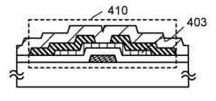
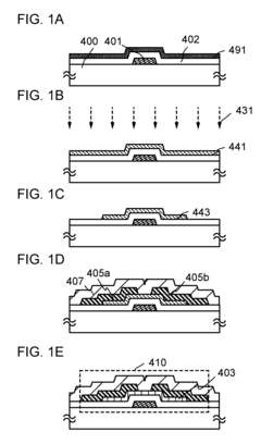
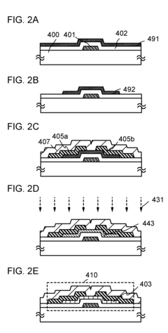
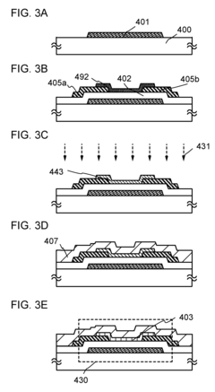
Semiconductor device and method for manufacturing the same
PatentActiveUS20160365454A1
Innovation
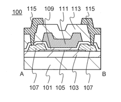
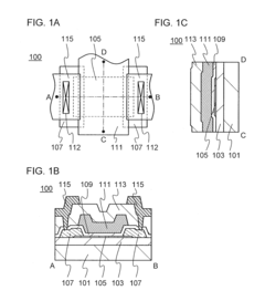
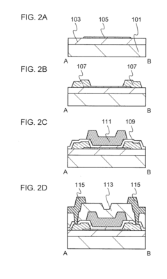
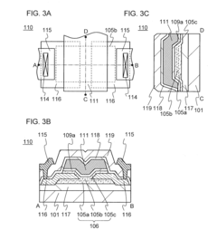
- The formation of an oxynitride insulating film with a higher oxygen content than stoichiometric composition using a CVD method with dinitrogen monoxide or nitrogen dioxide as oxidizing gases, which supplies oxygen to the oxide semiconductor film, reducing oxygen vacancies and interface states, thereby enhancing the on-state current and stability of the transistor.
Method for manufacturing semiconductor device
PatentInactiveUS20120295397A1
Innovation
- An amorphous oxide semiconductor film is formed with excess oxygen, covered with an aluminum oxide film, and subjected to heat treatment to crystallize, resulting in a crystalline oxide semiconductor film with a c-axis alignment, which stabilizes electrical characteristics and prevents impurity penetration.
Materials Compatibility and Integration Issues
The integration of oxide semiconductor films with existing device architectures presents significant materials compatibility challenges, particularly when considering the effects of oxygen vacancies. These vacancies, while essential for electrical conductivity in many oxide semiconductors, can create interfacial issues when these materials contact other device components.
When integrating oxide semiconductors with metal contacts, the formation of Schottky barriers at metal-semiconductor interfaces is heavily influenced by oxygen vacancy concentration. High vacancy densities near contact regions can lead to unpredictable barrier heights and contact resistances, compromising device performance reliability. Additionally, metals with high oxygen affinity (such as Ti, Al) can scavenge oxygen from the semiconductor layer, creating unintended vacancy profiles that extend beyond the immediate interface region.
Dielectric compatibility represents another critical integration concern. The deposition of gate dielectrics on oxide semiconductors can alter the vacancy distribution in the channel region. High-temperature deposition processes may drive oxygen diffusion, while plasma-enhanced processes can introduce additional defects. Conversely, oxygen from oxide dielectrics can diffuse into the semiconductor layer, potentially passivating beneficial vacancies and reducing carrier concentration in critical device regions.
Substrate selection significantly impacts vacancy formation and stability in oxide semiconductor films. Lattice mismatch between substrate and film can induce strain that modifies vacancy formation energy. Experimental studies have demonstrated that films grown on sapphire versus silicon substrates exhibit markedly different vacancy concentrations even under identical deposition conditions. Furthermore, oxygen diffusion from oxide substrates during high-temperature processing can alter the vacancy profile throughout the semiconductor layer.
Thermal budget constraints present particular challenges for integration. Post-deposition annealing treatments, commonly used to control vacancy concentration, must be compatible with the thermal stability limits of other device materials and structures. For instance, low-temperature polysilicon backplanes used in display technologies impose strict thermal constraints that limit vacancy engineering options for oxide semiconductor channels.
Encapsulation layers, essential for device stability, introduce additional compatibility considerations. These layers must prevent atmospheric oxygen and moisture from modifying vacancy concentrations while maintaining adhesion to the oxide semiconductor surface. Studies have shown that hydrogen-containing encapsulation materials can passivate oxygen vacancies, fundamentally altering semiconductor properties post-integration.
Environmental Impact of Oxide Semiconductor Manufacturing
The manufacturing processes of oxide semiconductor films, particularly those involving oxygen vacancy manipulation, present significant environmental challenges that warrant careful consideration. The production of these materials typically involves energy-intensive processes such as physical vapor deposition, chemical vapor deposition, and sputtering techniques, all of which contribute substantially to carbon emissions and resource consumption.
Primary environmental concerns stem from the use of toxic precursor materials in manufacturing processes. Metal-organic compounds, volatile organic compounds (VOCs), and various reactive gases employed in oxide semiconductor fabrication can lead to air pollution when improperly managed. Additionally, the etching processes often utilize hazardous acids and solvents that require specialized disposal protocols to prevent soil and water contamination.
Water usage represents another critical environmental factor, as semiconductor manufacturing facilities consume substantial quantities of ultra-pure water. The purification processes for this water are energy-intensive, and the resulting wastewater contains various contaminants that require treatment before discharge. Studies indicate that producing a single oxide semiconductor wafer may require hundreds of gallons of water, highlighting the significant water footprint of this industry.
The intentional creation of oxygen vacancies, while beneficial for semiconductor performance, introduces additional environmental complexities. These processes often require precisely controlled reducing atmospheres, sometimes utilizing hydrogen or other reducing gases that present both safety and environmental hazards if released. Furthermore, the energy requirements for maintaining these controlled atmospheres contribute to the overall carbon footprint of manufacturing.
Recent life cycle assessments of oxide semiconductor production reveal that the environmental impact extends beyond the manufacturing phase. The extraction of rare or precious metals used in certain high-performance oxide semiconductors involves mining operations with substantial ecological consequences, including habitat destruction and potential heavy metal contamination of surrounding ecosystems.
Industry response to these challenges has been evolving, with increasing implementation of closed-loop systems for chemical recovery and recycling. Advanced abatement systems for gaseous emissions have become standard in modern facilities, significantly reducing the release of harmful compounds. Additionally, research into more environmentally benign precursors and manufacturing methods shows promise for reducing the ecological footprint of oxide semiconductor production.
Regulatory frameworks worldwide are becoming more stringent regarding semiconductor manufacturing emissions and waste management. The European Union's Restriction of Hazardous Substances (RoHS) directive and similar regulations in other regions have pushed manufacturers toward developing greener processes and substituting hazardous materials where possible.
Unlock deeper insights with Patsnap Eureka Quick Research — get a full tech report to explore trends and direct your research. Try now!
Generate Your Research Report Instantly with AI Agent
Supercharge your innovation with Patsnap Eureka AI Agent Platform!
