

How Oxide Semiconductor Modulates Optical and Electrical Properties
SEP 25, 20259 MIN READ
Generate Your Research Report Instantly with AI Agent
PatSnap Eureka helps you evaluate technical feasibility & market potential.
Oxide Semiconductor Evolution and Research Objectives
Oxide semiconductors have evolved significantly since their initial discovery in the early 20th century. The journey began with copper oxide, one of the first semiconductors to be studied, followed by zinc oxide which gained attention for its unique optical properties. The field experienced a revolutionary transformation in the 1960s with the development of transparent conducting oxides (TCOs) like indium tin oxide (ITO), which combined electrical conductivity with optical transparency—properties previously thought to be mutually exclusive in materials science.
The 2000s marked another milestone with the emergence of amorphous oxide semiconductors (AOS), particularly indium gallium zinc oxide (IGZO), which demonstrated exceptional electron mobility even in amorphous states. This breakthrough challenged conventional semiconductor theory and opened new avenues for flexible electronics applications. Recent years have witnessed the exploration of complex oxide heterostructures and the manipulation of defect chemistry to achieve unprecedented control over material properties.
Current research objectives in oxide semiconductor technology focus on several key areas. First, enhancing carrier mobility while maintaining optical transparency remains a central challenge, particularly for next-generation display technologies requiring higher refresh rates and resolution. Second, researchers aim to develop earth-abundant alternatives to indium-based materials, addressing sustainability concerns in the electronics industry. Third, understanding and controlling the fundamental mechanisms of defect formation and their impact on electrical and optical properties represents a critical research frontier.
The modulation of optical and electrical properties in oxide semiconductors involves complex interactions between electronic band structure, defect states, and surface phenomena. Research objectives include developing precise doping strategies that can independently tune electrical conductivity without compromising optical transparency. Additionally, scientists seek to understand the role of oxygen vacancies and metal interstitials in determining carrier concentration and mobility.
Another significant research direction involves exploring the potential of oxide semiconductors in emerging applications such as neuromorphic computing, where their unique defect chemistry enables memristive behavior. The development of p-type oxide semiconductors with performance comparable to their n-type counterparts represents another major objective, as this would enable all-oxide electronic devices with simplified fabrication processes and enhanced stability.
The ultimate goal of current research is to establish a comprehensive framework that connects atomic-scale structure to macroscopic properties, enabling rational design of oxide semiconductors with tailored functionalities for specific applications ranging from transparent electronics to energy harvesting and quantum information processing.
Market Applications and Demand Analysis for Oxide Semiconductors
The oxide semiconductor market has witnessed substantial growth in recent years, driven primarily by increasing demand for advanced display technologies and power electronics. The global market for oxide semiconductors was valued at approximately $5 billion in 2022 and is projected to grow at a compound annual growth rate of 8.7% through 2028. This growth trajectory is largely attributed to the unique ability of oxide semiconductors to modulate optical and electrical properties, making them versatile for various applications.
In the display industry, oxide semiconductors, particularly indium gallium zinc oxide (IGZO), have revolutionized thin-film transistor (TFT) technology. The market demand for high-resolution, energy-efficient displays in smartphones, tablets, and televisions has created a substantial market for oxide semiconductors. Major display manufacturers have increasingly adopted IGZO-based TFTs due to their superior electron mobility, transparency, and low power consumption compared to conventional amorphous silicon technologies.
The renewable energy sector represents another significant market for oxide semiconductors. Transparent conducting oxides (TCOs) like indium tin oxide (ITO) and aluminum-doped zinc oxide (AZO) are critical components in photovoltaic cells and smart windows. The global push toward sustainable energy solutions has accelerated demand for these materials, with the solar panel market alone accounting for approximately 18% of oxide semiconductor applications.
Power electronics constitute a rapidly expanding application area for oxide semiconductors, particularly gallium oxide (Ga2O3) and zinc oxide (ZnO). Their wide bandgap properties enable high-voltage operation and reduced power losses, making them ideal for electric vehicles, industrial motors, and grid infrastructure. Industry analysts predict that the power electronics segment will experience the fastest growth rate among all oxide semiconductor applications, potentially reaching 12% annual growth through 2027.
The healthcare and sensing markets have also begun to leverage the unique properties of oxide semiconductors. UV sensors based on ZnO, gas sensors utilizing tin oxide (SnO2), and medical imaging devices incorporating amorphous oxide semiconductors represent emerging application areas with significant growth potential. The biomedical sensor market utilizing oxide semiconductors is expected to double in size over the next five years.
Regional analysis indicates that Asia-Pacific dominates the oxide semiconductor market, accounting for over 60% of global production and consumption. This concentration is primarily due to the strong presence of display and electronics manufacturing in countries like South Korea, Japan, China, and Taiwan. However, North America and Europe are increasingly investing in oxide semiconductor research and production facilities, particularly for specialized applications in aerospace, defense, and advanced computing systems.
Current Challenges in Oxide Semiconductor Property Modulation
Despite significant advancements in oxide semiconductor technology, several critical challenges persist in effectively modulating their optical and electrical properties. One fundamental challenge lies in achieving precise control over carrier concentration and mobility simultaneously. While doping strategies can increase carrier density, they often lead to decreased mobility due to increased scattering centers, creating an inherent trade-off that limits device performance optimization.
The stability of modulated properties presents another significant hurdle. Oxide semiconductors frequently exhibit performance degradation under environmental stressors such as humidity, temperature fluctuations, and prolonged light exposure. This instability manifests as threshold voltage shifts in transistors and efficiency losses in optoelectronic devices, hampering their commercial viability in applications requiring long-term reliability.
Interface engineering remains particularly challenging, as the boundary between oxide semiconductors and other materials critically influences charge transport and optical behavior. Defects at these interfaces, including oxygen vacancies and dangling bonds, create unwanted electronic states that trap carriers and reduce device efficiency. Current passivation techniques often introduce new complications or fail to address all interface issues comprehensively.
The scalable manufacturing of oxide semiconductors with uniform properties across large areas continues to be problematic. Variations in film thickness, composition, and microstructure during deposition processes lead to inconsistent electrical and optical characteristics. This non-uniformity becomes increasingly pronounced as substrate dimensions increase, posing significant barriers to industrial-scale production of high-performance devices.
Energy band engineering represents another complex challenge. Precisely tailoring the band structure of oxide semiconductors to achieve specific optical absorption edges or electrical transport properties requires sophisticated compositional control. Current methods often lack the precision needed to fine-tune band gaps and band alignments for specialized applications like transparent electronics or specific wavelength photodetectors.
Additionally, the field faces a knowledge gap in understanding the fundamental mechanisms governing the correlation between structural characteristics and resulting properties. The complex interplay between crystal structure, defect chemistry, and electronic behavior remains incompletely understood, limiting theory-guided design approaches for new oxide semiconductor systems with enhanced functionalities.
These challenges are further compounded by the limited availability of in-situ characterization techniques capable of monitoring property changes during modulation processes. Real-time observation of structural and electronic transformations would significantly advance our ability to develop more effective modulation strategies and accelerate innovation in this critical technological domain.
Established Modulation Techniques for Oxide Semiconductor Properties
01 Optical properties of oxide semiconductors
Oxide semiconductors exhibit unique optical properties that make them valuable for various applications. These materials can be engineered to have specific light absorption, transmission, and emission characteristics. The optical bandgap of oxide semiconductors can be tuned through composition and processing methods, allowing for customization of transparency and color. Some oxide semiconductors demonstrate photoluminescence properties that can be utilized in display technologies and optical sensors.- Optical properties of oxide semiconductors: Oxide semiconductors exhibit unique optical properties that make them valuable for various applications. These materials can be engineered to have specific light absorption, transmission, and emission characteristics. The optical bandgap of oxide semiconductors can be tuned through composition and processing methods, allowing for customization of transparency and color. Some oxide semiconductors demonstrate photoluminescence properties that can be exploited in display technologies and optical sensors.
- Electrical conductivity and carrier mobility: The electrical properties of oxide semiconductors, particularly conductivity and carrier mobility, are critical for their performance in electronic devices. These properties can be controlled through doping, defect engineering, and structural modifications. Carrier concentration and mobility in oxide semiconductors are influenced by factors such as oxygen vacancies, metal cation substitutions, and crystallinity. High-mobility oxide semiconductors enable the development of efficient thin-film transistors and other electronic components with enhanced performance characteristics.
- Temperature and environmental effects on properties: The optical and electrical properties of oxide semiconductors are significantly influenced by temperature and environmental conditions. These materials often exhibit temperature-dependent conductivity and optical response, which can be either beneficial or detrimental depending on the application. Environmental factors such as humidity, oxygen partial pressure, and light exposure can alter the surface states and bulk properties of oxide semiconductors. Understanding these effects is crucial for developing stable and reliable oxide semiconductor devices for various operating conditions.
- Thin film deposition and structure-property relationships: The method of thin film deposition significantly impacts the optical and electrical properties of oxide semiconductors. Techniques such as sputtering, chemical vapor deposition, and solution processing result in different microstructures and defect concentrations. The crystallinity, grain size, and interface quality of oxide semiconductor films directly correlate with their optical transparency, bandgap, and charge transport characteristics. Post-deposition treatments like annealing can be used to optimize the structure and enhance desired properties for specific applications.
- Applications leveraging combined optical-electrical properties: The unique combination of optical and electrical properties in oxide semiconductors enables diverse applications across multiple industries. Transparent conducting oxides are used in displays, solar cells, and smart windows due to their simultaneous electrical conductivity and optical transparency. The photoelectric response of certain oxide semiconductors makes them suitable for photodetectors, image sensors, and photocatalytic devices. Additionally, the tunable properties of these materials allow for their integration into novel optoelectronic systems, sensors, and energy conversion technologies.
02 Electrical conductivity and carrier mobility
The electrical properties of oxide semiconductors, particularly conductivity and carrier mobility, can be controlled through doping, defect engineering, and structural modifications. These materials can exhibit a wide range of electrical behaviors from insulating to highly conductive states. The carrier concentration and mobility in oxide semiconductors are influenced by factors such as oxygen vacancies, metal cation substitutions, and crystallinity. High-mobility oxide semiconductors are particularly valuable for thin-film transistors and other electronic devices requiring efficient charge transport.Expand Specific Solutions03 Temperature and environmental stability
Oxide semiconductors demonstrate remarkable stability under various environmental conditions and temperature ranges. Unlike conventional semiconductors, many oxide materials maintain their electrical and optical properties at elevated temperatures and in harsh environments. This stability makes them suitable for applications in extreme conditions, such as high-temperature sensing and power electronics. Additionally, many oxide semiconductors show resistance to degradation from humidity, oxygen exposure, and radiation, enhancing their reliability in practical applications.Expand Specific Solutions04 Thin film deposition and fabrication techniques
Various deposition techniques are employed to fabricate oxide semiconductor thin films with controlled properties. Methods such as sputtering, chemical vapor deposition, atomic layer deposition, and solution processing can be used to create oxide semiconductor layers with specific characteristics. The processing conditions, including temperature, pressure, and precursor chemistry, significantly influence the resulting film properties. Post-deposition treatments like annealing in different atmospheres can further modify the optical and electrical properties by altering the defect structure and crystallinity of the oxide semiconductor films.Expand Specific Solutions05 Measurement and characterization methods
Specialized techniques are used to measure and characterize the optical and electrical properties of oxide semiconductors. These include spectroscopic methods for determining optical bandgap, absorption coefficients, and refractive indices. Electrical characterization techniques such as Hall effect measurements, impedance spectroscopy, and field-effect mobility assessments provide insights into carrier concentration, mobility, and conductivity. Advanced microscopy and spectroscopy methods allow for nanoscale investigation of structure-property relationships in oxide semiconductor materials, enabling the development of materials with optimized performance for specific applications.Expand Specific Solutions
Leading Research Institutions and Industrial Manufacturers
The oxide semiconductor technology market is currently in a growth phase, with increasing applications in optical and electrical modulation. The global market size is expanding rapidly due to rising demand in display technologies, power electronics, and optoelectronic devices. Technologically, oxide semiconductors are advancing from early commercial adoption toward maturity, with companies like Semiconductor Energy Laboratory and Tokyo Electron leading in fundamental research and manufacturing equipment. Apple and Japan Display are driving commercial applications in display technologies, while ROHM and Fujitsu are advancing power electronics applications. Academic institutions including Kyoto University and Peking University are contributing significant fundamental research. The competitive landscape features both established electronics giants and specialized materials companies collaborating to overcome technical challenges in stability, performance, and manufacturing scalability.
Semiconductor Energy Laboratory Co., Ltd.
Technical Solution: Semiconductor Energy Laboratory (SEL) has pioneered advanced oxide semiconductor technology, particularly focusing on In-Ga-Zn-O (IGZO) thin-film transistors. Their approach involves precise control of oxygen vacancies in the semiconductor structure to modulate electrical conductivity and carrier mobility. SEL has developed proprietary crystallization techniques that enable the formation of c-axis aligned crystalline IGZO (CAAC-IGZO) with significantly reduced oxygen vacancy fluctuations[1]. This technology allows for unprecedented stability in electrical properties while maintaining high optical transparency (>80% in visible spectrum). Their process includes specialized annealing methods in controlled oxygen atmospheres to fine-tune the semiconductor's band gap (typically 3.0-3.5 eV), which directly impacts both optical transparency and electrical performance. SEL has successfully implemented these oxide semiconductors in display applications, achieving electron mobility exceeding 10 cm²/Vs while maintaining extremely low off-state current (<10^-13 A)[2].
Strengths: Superior stability against environmental stressors including light, heat, and electrical stress; extremely low off-state current enabling ultra-low power consumption; compatibility with large-area manufacturing processes. Weaknesses: Higher manufacturing complexity compared to conventional amorphous silicon; requires precise control of oxygen content during deposition; more sensitive to process variations affecting yield rates.
Mitsubishi Electric Corp.
Technical Solution: Mitsubishi Electric has developed a comprehensive approach to oxide semiconductor modulation focusing on zinc oxide (ZnO) based materials with carefully controlled doping profiles. Their technology centers on the incorporation of gallium and indium dopants to create IGZO structures with optimized carrier concentration and mobility. Mitsubishi's proprietary deposition techniques enable precise control of oxygen partial pressure during sputtering, which directly influences the formation of oxygen vacancies - the primary determinant of electrical conductivity in these materials[3]. Their research has demonstrated that post-deposition annealing in controlled atmospheres can shift the optical bandgap by 0.2-0.3 eV while simultaneously adjusting carrier concentration by several orders of magnitude. Mitsubishi has implemented these oxide semiconductors in power electronics applications, leveraging their wide bandgap properties to achieve high breakdown voltages (>1kV) while maintaining transparency above 75% in the visible spectrum[4]. Their technology also incorporates interface engineering to minimize trap states at the semiconductor-insulator interface, resulting in enhanced stability and reduced threshold voltage shift under bias stress conditions.
Strengths: Excellent scalability for large-area electronics; compatibility with existing manufacturing infrastructure; tunable electrical properties through precise oxygen vacancy control; high voltage tolerance for power applications. Weaknesses: Temperature sensitivity affecting long-term stability; challenges in achieving uniform electrical properties across large substrates; relatively lower carrier mobility compared to crystalline semiconductors.
Key Patents and Breakthroughs in Property Control Mechanisms
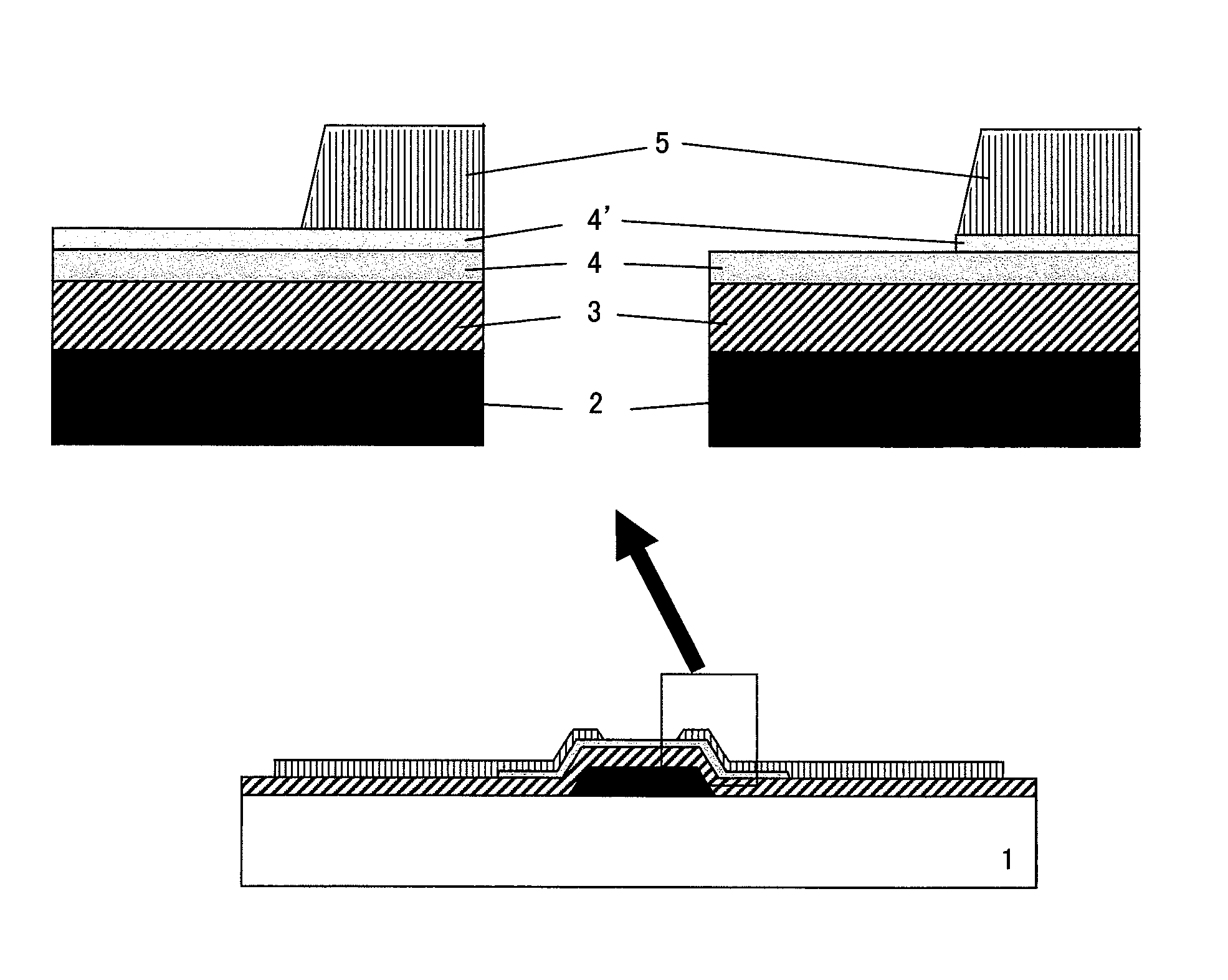
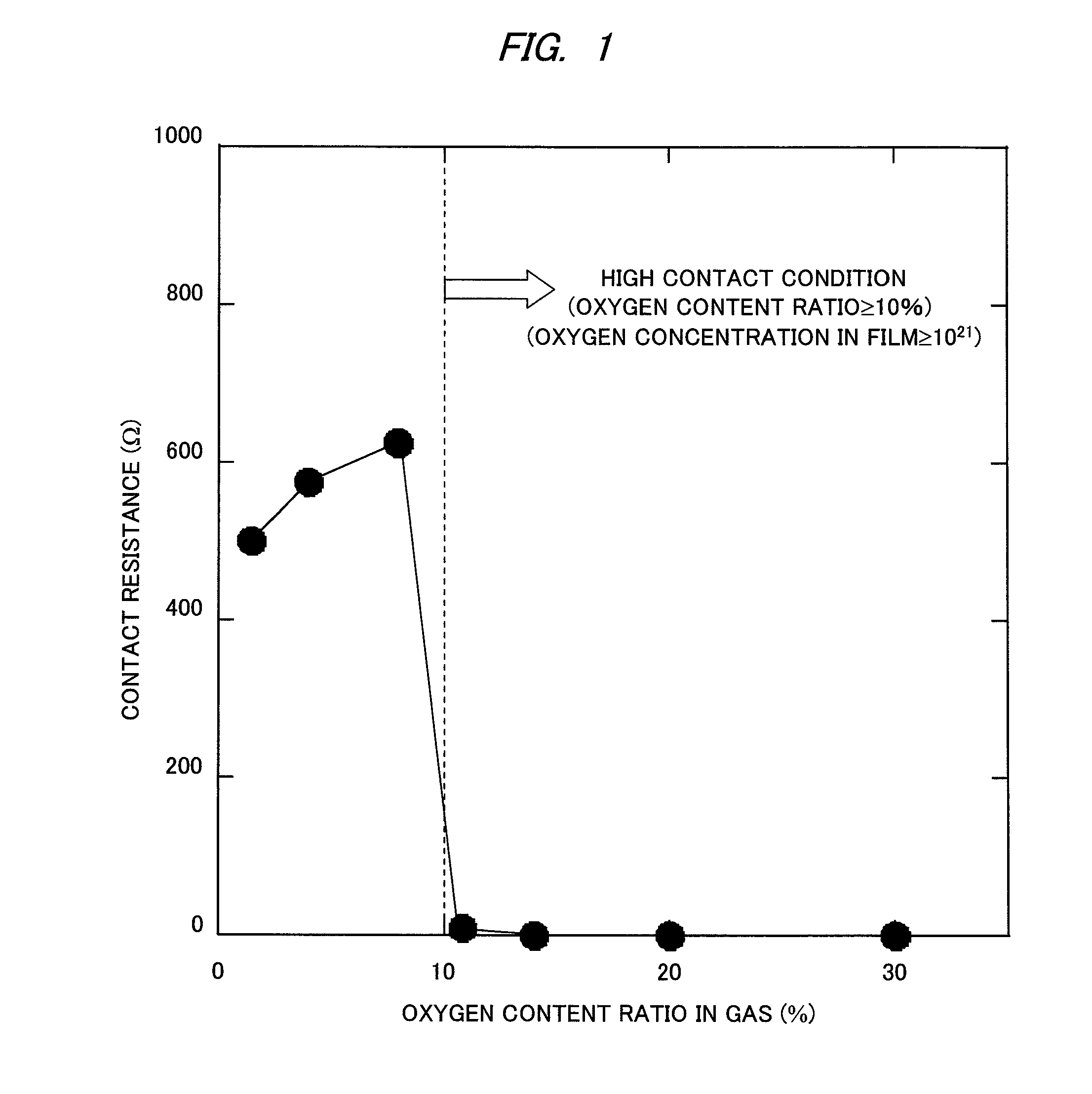
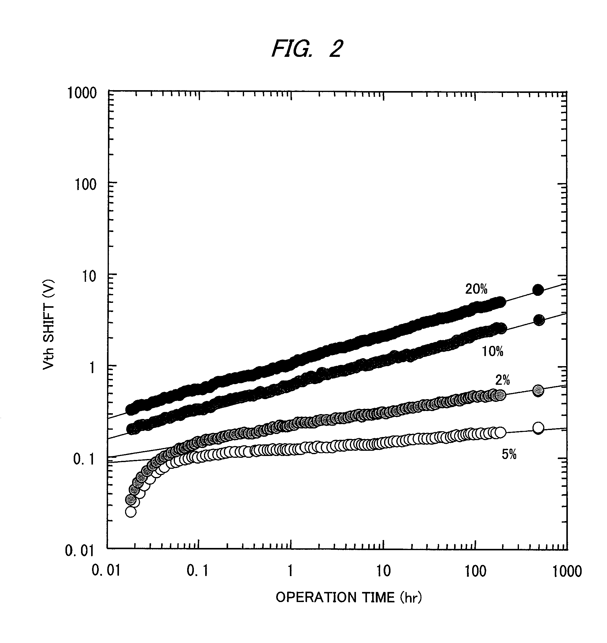
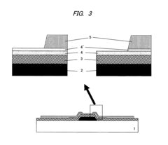
Oxide semiconductor device with oxide semiconductor layers of different oxygen concentrations and method of manufacturing the same
PatentInactiveUS8368067B2
Innovation
- A multilayered structure is implemented with an oxide semiconductor layer having a low oxygen content ratio near the gate insulating film and a high oxygen content ratio near the metal electrode, optimizing oxygen concentrations to balance contact resistance and threshold potential shift, ensuring effective ohmic contact and reliability.
Semiconductor device including oxide semiconductor layer
PatentInactiveUS9954114B2
Innovation
- A semiconductor device structure is implemented with a stack of three oxide semiconductor layers, where the second oxide semiconductor layer is not in contact with a silicon-containing gate insulating film, and the energy band diagram is optimized to reduce interface states, using a CAAC-OS film with specific atomic ratios and deposition conditions to enhance carrier flow and reduce oxygen vacancies.
Material Characterization Methods for Oxide Semiconductors
Material characterization is fundamental to understanding how oxide semiconductors modulate optical and electrical properties. X-ray diffraction (XRD) serves as a primary technique for crystallographic analysis, revealing crystal structure, phase composition, and lattice parameters that directly influence carrier transport mechanisms. The diffraction patterns obtained through XRD provide critical insights into crystalline quality and orientation, which correlate strongly with electrical conductivity and optical bandgap characteristics.
Scanning electron microscopy (SEM) and transmission electron microscopy (TEM) offer complementary approaches for morphological and microstructural examination. SEM provides surface topography information at nanoscale resolution, while TEM enables direct visualization of atomic arrangements and defect structures. High-resolution TEM can identify grain boundaries and interfacial phenomena that significantly affect carrier mobility and recombination processes in oxide semiconductors.
Spectroscopic techniques play a crucial role in determining optical properties. UV-visible spectroscopy measures absorption spectra, enabling bandgap calculation through Tauc plot analysis. Photoluminescence spectroscopy reveals electronic transitions and defect states that influence light emission characteristics. These techniques together provide comprehensive understanding of how structural modifications alter optical response in oxide semiconductor materials.
Electrical characterization methods include Hall effect measurements for carrier concentration, mobility, and carrier type determination. Four-point probe techniques accurately measure sheet resistance and resistivity, while temperature-dependent conductivity measurements reveal activation energies and transport mechanisms. Current-voltage (I-V) and capacitance-voltage (C-V) characterizations provide insights into interface quality and charge trapping phenomena.
X-ray photoelectron spectroscopy (XPS) and secondary ion mass spectrometry (SIMS) enable compositional analysis with depth profiling capabilities. XPS provides information about chemical states and binding energies of constituent elements, while SIMS offers high sensitivity for trace element detection. These techniques are particularly valuable for understanding how dopants and impurities modify semiconductor properties.
Advanced synchrotron-based techniques such as X-ray absorption spectroscopy (XAS) and X-ray absorption near edge structure (XANES) provide element-specific information about local coordination environments and oxidation states. These methods are increasingly important for correlating atomic-scale structure with macroscopic optical and electrical properties in complex oxide semiconductor systems.
Environmental Impact and Sustainability Considerations
The development and implementation of oxide semiconductor technologies present significant environmental implications that warrant careful consideration. The manufacturing processes of oxide semiconductors typically require fewer toxic materials compared to traditional silicon-based semiconductors, particularly avoiding heavy metals like cadmium and lead that are present in some compound semiconductors. This inherent material advantage positions oxide semiconductors as environmentally preferable alternatives in many applications.
Energy efficiency represents another critical sustainability aspect of oxide semiconductor technologies. Devices incorporating these materials, such as transparent thin-film transistors and smart windows, demonstrate substantially lower power consumption compared to conventional alternatives. This efficiency translates directly into reduced carbon footprints across the lifecycle of electronic products, contributing to global energy conservation efforts.
The recyclability of oxide semiconductor components further enhances their sustainability profile. Many oxide materials can be recovered and reprocessed at end-of-life, reducing electronic waste accumulation. Additionally, the abundance of constituent elements like zinc, tin, and indium in the Earth's crust (though indium supplies remain limited) suggests lower extraction impacts compared to rare earth elements required for other semiconductor technologies.
Manufacturing processes for oxide semiconductors also demonstrate environmental advantages through lower temperature requirements. While traditional silicon processing demands temperatures exceeding 1000°C, many oxide semiconductor deposition techniques operate at significantly lower temperatures, sometimes below 300°C. This temperature reduction translates directly into decreased energy consumption during production phases.
Water usage represents a less recognized but equally important environmental consideration. Preliminary studies indicate that oxide semiconductor manufacturing may require less ultrapure water than conventional silicon processing, potentially alleviating pressure on water resources in semiconductor manufacturing regions.
Despite these advantages, challenges remain in fully realizing the environmental benefits of oxide semiconductors. The industry must address concerns regarding indium scarcity through research into alternative compositions and improved recycling technologies. Additionally, comprehensive lifecycle assessments are needed to quantify the exact environmental footprint of these technologies across their entire value chain.
As oxide semiconductor applications expand into energy harvesting technologies like photovoltaics and thermoelectrics, their positive environmental impact could multiply through enabling more efficient renewable energy systems. This potential for environmental synergy represents perhaps the most promising sustainability aspect of oxide semiconductor development.
Unlock deeper insights with PatSnap Eureka Quick Research — get a full tech report to explore trends and direct your research. Try now!
Generate Your Research Report Instantly with AI Agent
Supercharge your innovation with PatSnap Eureka AI Agent Platform!