How Oxide Semiconductor Influences Electron Transport Mechanisms
SEP 25, 20259 MIN READ
Generate Your Research Report Instantly with AI Agent
Patsnap Eureka helps you evaluate technical feasibility & market potential.
Oxide Semiconductor Evolution and Research Objectives
Oxide semiconductors have evolved significantly since their initial discovery in the early 20th century. The journey began with cuprous oxide (Cu2O) in the 1920s, which was used in early rectifiers and photovoltaic cells. However, the field remained relatively dormant until the 1960s when transparent conducting oxides (TCOs) like indium tin oxide (ITO) emerged as critical materials for optoelectronic applications. The true revolution came in the early 2000s with the development of amorphous oxide semiconductors (AOS), particularly indium gallium zinc oxide (IGZO), which demonstrated unprecedented combinations of high electron mobility and optical transparency.
The evolution of oxide semiconductors has been driven by the fundamental understanding of their unique electronic structure. Unlike conventional semiconductors based on sp3 hybridization, oxide semiconductors feature metal cations with spherically symmetric s-orbitals forming the conduction band minimum. This distinctive band structure enables high electron mobility even in amorphous states, a property that has transformed display technologies and enabled flexible electronics.
Recent advancements have expanded beyond binary oxides to complex multi-component systems, allowing precise tuning of electronic properties through compositional engineering. The incorporation of dopants and the development of heterostructures have further enhanced performance characteristics, enabling applications ranging from high-performance thin-film transistors to neuromorphic computing elements.
The current research landscape is focused on understanding and controlling electron transport mechanisms across different oxide semiconductor systems. Particular attention is being paid to the role of oxygen vacancies, which act as native donors and significantly influence carrier concentration and mobility. The interplay between structural disorder, defect states, and electronic transport remains a central challenge in optimizing device performance.
Research objectives in this field are multifaceted and interdisciplinary. Primary goals include elucidating the fundamental physics governing electron transport in various oxide semiconductor structures, from crystalline to amorphous phases. Researchers aim to develop predictive models that can accurately describe carrier generation, recombination, and transport phenomena across different material compositions and morphologies.
Another critical objective is to establish clear structure-property relationships that connect atomic arrangements to macroscopic electronic properties. This includes understanding how factors such as cation coordination, oxygen stoichiometry, and structural disorder influence band structure, effective mass, and scattering mechanisms. Such knowledge is essential for designing next-generation oxide semiconductors with tailored electronic properties for specific applications.
Market Applications and Industry Demand Analysis
The oxide semiconductor market has witnessed substantial growth in recent years, driven primarily by the expanding display technology sector. The global market for oxide semiconductors reached approximately $5.2 billion in 2022 and is projected to grow at a compound annual growth rate of 8.7% through 2028. This growth is largely attributed to the superior electron transport properties of oxide semiconductors, particularly in thin-film transistor (TFT) applications where they offer enhanced mobility and stability compared to conventional amorphous silicon.
The display industry represents the largest market segment for oxide semiconductors, accounting for over 65% of total demand. Indium gallium zinc oxide (IGZO) has emerged as the dominant material in this sector, being widely adopted in high-resolution displays for smartphones, tablets, and large-format televisions. Major display manufacturers including Samsung, LG Display, and BOE Technology have significantly increased their investment in oxide semiconductor technology, recognizing its potential to enable next-generation display products with lower power consumption and higher pixel densities.
Beyond displays, the semiconductor industry has shown growing interest in oxide semiconductors for power electronics applications. The wide bandgap characteristics and high breakdown voltage of materials like gallium oxide (Ga2O3) make them particularly suitable for high-power switching devices. Market analysis indicates that the power electronics segment for oxide semiconductors is growing at 12.3% annually, outpacing the overall market growth rate.
The healthcare and medical imaging sectors represent emerging markets for oxide semiconductors, particularly for X-ray imaging detectors where amorphous oxide semiconductors demonstrate superior performance in large-area sensing applications. This segment is expected to grow significantly as healthcare facilities worldwide upgrade to digital imaging systems.
Geographic distribution of market demand shows Asia-Pacific leading with approximately 68% of global consumption, followed by North America (15%) and Europe (12%). China, South Korea, Japan, and Taiwan collectively account for over 55% of global demand, reflecting the concentration of display and electronics manufacturing in these regions.
Industry surveys indicate that manufacturers are increasingly prioritizing research into electron transport mechanisms in oxide semiconductors to overcome current limitations in mobility and stability. Approximately 78% of industry respondents identified improved understanding of transport mechanisms as "critical" or "very important" for next-generation product development, highlighting the direct connection between fundamental research in this area and commercial applications.
Current State and Technical Barriers in Electron Transport
Oxide semiconductor technology has witnessed significant advancements in recent years, revolutionizing electron transport mechanisms across various electronic applications. Currently, the field is dominated by materials such as Indium Gallium Zinc Oxide (IGZO), Zinc Tin Oxide (ZTO), and Hafnium Indium Zinc Oxide (HIZO), which have demonstrated superior electron mobility compared to traditional amorphous silicon. These materials exhibit carrier mobilities ranging from 10-50 cm²/Vs, approximately 10 times higher than a-Si:H, while maintaining excellent uniformity over large areas.
Despite these achievements, several technical barriers impede further development in oxide semiconductor electron transport. The most significant challenge remains the trade-off between carrier concentration and mobility. High carrier concentrations often lead to increased scattering events, thereby reducing overall mobility. This fundamental limitation has constrained the performance ceiling of oxide semiconductor devices, particularly in high-frequency applications requiring both high conductivity and mobility.
Oxygen vacancy management represents another critical barrier. These vacancies serve as electron donors in oxide semiconductors but simultaneously create trap states that impede electron transport. Current fabrication techniques struggle to achieve precise control over oxygen vacancy concentration, resulting in inconsistent device performance and reliability issues. Advanced deposition methods such as atomic layer deposition (ALD) show promise but face scalability challenges for mass production.
Interface engineering presents a persistent challenge, as electron transport is significantly affected by the quality of interfaces between the semiconductor and adjacent layers. Current research indicates that up to 70% of electron mobility degradation occurs due to interface scattering phenomena. While surface passivation techniques have improved interface quality, achieving atomically smooth interfaces with minimal defect density remains elusive at industrial scales.
Temperature stability constitutes another major technical barrier. Most oxide semiconductors exhibit significant variations in electron transport properties across operating temperature ranges. This thermal instability manifests as threshold voltage shifts and mobility fluctuations, limiting their application in environments with variable thermal conditions. Recent developments in compositional engineering have improved thermal stability, but complete temperature independence has not yet been achieved.
The scaling limitations of oxide semiconductors also present challenges for next-generation nanoelectronics. As device dimensions approach the nanoscale, quantum confinement effects begin to dominate electron transport mechanisms, necessitating new models beyond classical semiconductor physics. Current understanding of quantum transport in oxide semiconductors remains limited, hampering the development of ultra-scaled devices.
Globally, research efforts are concentrated in East Asia, particularly Japan, South Korea, and Taiwan, where major display manufacturers have established significant intellectual property portfolios. European and North American institutions focus more on fundamental transport mechanisms and novel material compositions, creating a geographically diverse but somewhat fragmented research landscape.
Contemporary Approaches to Enhancing Electron Mobility
01 Charge carrier transport mechanisms in oxide semiconductors
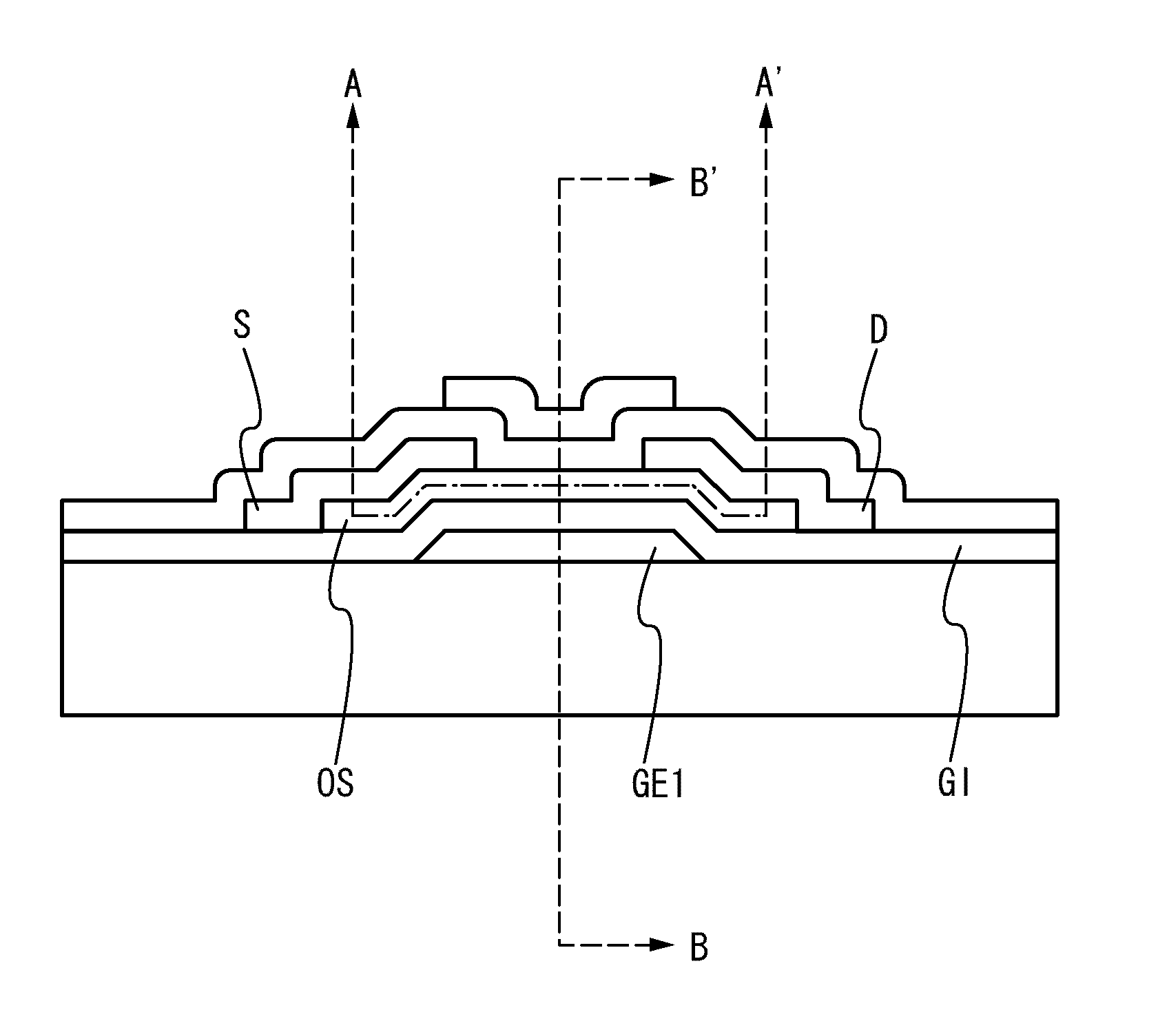
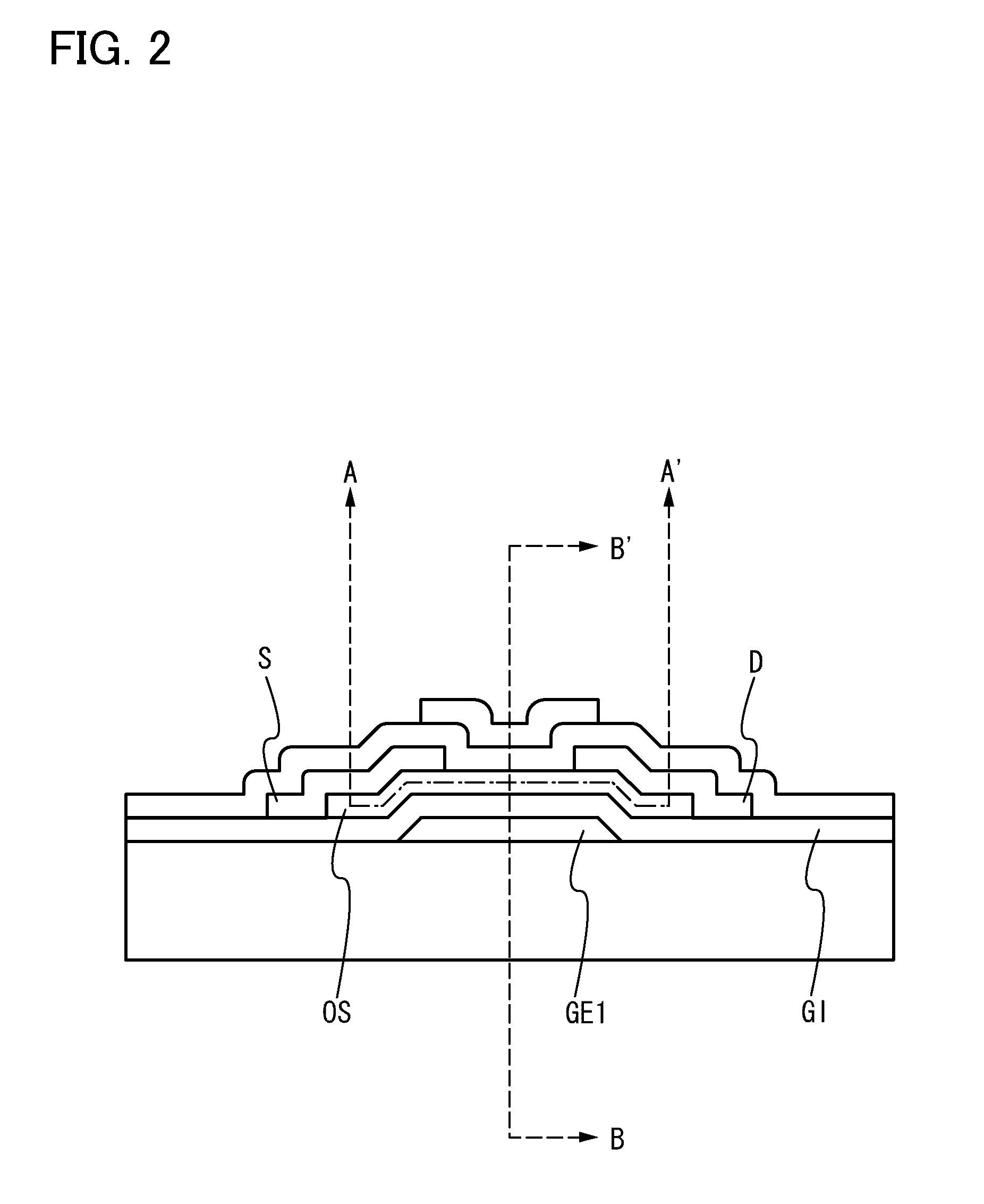
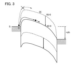
Oxide semiconductors exhibit unique electron transport mechanisms characterized by the movement of charge carriers through the material. These mechanisms involve electron hopping between localized states, band transport through extended states, and tunneling through potential barriers. The transport properties are influenced by the electronic band structure, defect states, and carrier concentration, which can be engineered to optimize device performance. Understanding these fundamental transport mechanisms is crucial for developing high-performance oxide semiconductor devices.- Band structure and carrier transport in oxide semiconductors: The electron transport mechanism in oxide semiconductors is largely determined by their band structure. These materials typically have a wide bandgap and high electron mobility. The conduction band is formed primarily by metal s-orbitals, which creates dispersed energy bands that facilitate electron transport. Factors such as oxygen vacancies, metal interstitials, and doping can significantly influence the carrier concentration and mobility by modifying the band structure and creating additional energy states within the bandgap.
- Defect-mediated electron transport mechanisms: Defects play a crucial role in electron transport within oxide semiconductors. Oxygen vacancies, which act as shallow donors, contribute to n-type conductivity by releasing electrons into the conduction band. Metal interstitials and substitutional impurities can also serve as electron donors or acceptors. The spatial distribution and concentration of these defects significantly impact the electron transport pathways, creating localized states that can either enhance conductivity through hopping mechanisms or act as scattering centers that reduce mobility.
- Interface and grain boundary effects on electron transport: Interfaces and grain boundaries significantly influence electron transport in oxide semiconductor devices. These structural features can create potential barriers, trap states, and depletion regions that electrons must overcome. In thin-film transistors, the semiconductor-dielectric interface quality directly affects channel mobility and threshold voltage stability. Grain boundaries in polycrystalline oxide semiconductors act as scattering centers and trap sites, limiting electron mobility. Engineering these interfaces through surface treatments, buffer layers, or controlled crystallization can optimize electron transport properties.
- Environmental and operational stability of electron transport: The electron transport mechanisms in oxide semiconductors are sensitive to environmental factors and operational conditions. Exposure to oxygen, moisture, light, and temperature can modify the surface states and bulk defect concentrations, affecting carrier density and mobility. Under bias stress, charge trapping at interfaces or in bulk defects can cause threshold voltage shifts and mobility degradation. Passivation layers, optimized annealing processes, and compositional tuning are employed to enhance the stability of electron transport properties under various environmental and operational conditions.
- Advanced oxide semiconductor compositions for enhanced electron transport: Innovative compositional engineering of oxide semiconductors has led to enhanced electron transport properties. Multi-component oxides, such as indium-gallium-zinc oxide (IGZO), indium-zinc oxide (IZO), and zinc-tin oxide (ZTO), offer tunable electronic properties through compositional adjustment. Doping with elements like hydrogen, nitrogen, or rare earth metals can modify the band structure and defect chemistry. Additionally, creating heterostructures and quantum well structures allows for band engineering that can confine and direct electron flow, resulting in higher mobility and better-controlled transport characteristics.
02 Defect engineering and doping effects on electron mobility
Defect engineering and doping significantly impact electron transport in oxide semiconductors. Oxygen vacancies, metal interstitials, and substitutional dopants create energy states within the bandgap that affect carrier concentration and mobility. Controlled doping can enhance conductivity by introducing additional charge carriers, while defect management can reduce scattering centers that impede electron movement. These approaches allow for tailoring the electronic properties of oxide semiconductors to meet specific application requirements, such as high mobility for transistors or controlled carrier density for sensors.Expand Specific Solutions03 Interface and surface effects on electron transport
The interfaces between oxide semiconductors and adjacent materials significantly influence electron transport properties. Surface states, band bending, and potential barriers at interfaces can create depletion regions or accumulation layers that modify carrier concentration profiles. These interface phenomena affect charge injection, extraction, and transport across device structures. Engineering interface properties through surface treatments, buffer layers, or contact materials optimization is essential for improving device performance by reducing contact resistance and enhancing carrier transport across heterojunctions.Expand Specific Solutions04 Temperature and environmental dependence of transport mechanisms
Electron transport mechanisms in oxide semiconductors exhibit strong temperature and environmental dependencies. At different temperature regimes, various transport mechanisms dominate, including band-like transport at low temperatures and thermally activated hopping at higher temperatures. Environmental factors such as humidity, oxygen partial pressure, and light exposure can modify surface states and bulk defect concentrations, altering carrier densities and transport properties. Understanding these dependencies is crucial for designing devices with stable performance across operating conditions and for developing sensing applications that leverage these environmental sensitivities.Expand Specific Solutions05 Advanced oxide semiconductor structures for enhanced electron transport
Novel oxide semiconductor structures have been developed to enhance electron transport properties. These include multi-component oxide systems, quantum well structures, superlattices, and nanostructured materials that exploit quantum confinement effects. By engineering the material composition, crystal structure, and dimensionality, these advanced structures can achieve higher carrier mobilities, reduced scattering, and improved stability. The controlled growth of crystalline oxide films with minimal defects and optimized interfaces enables superior electron transport characteristics for high-performance electronic and optoelectronic applications.Expand Specific Solutions
Leading Research Institutions and Industrial Manufacturers
The oxide semiconductor field is currently in a growth phase, with market size expanding due to increasing applications in display technologies and electronics. The technology maturity varies across different segments, with companies like Semiconductor Energy Laboratory, Samsung Electronics, and Japan Display leading in IGZO (Indium Gallium Zinc Oxide) technology development. Major players including Sony, Huawei, and GLOBALFOUNDRIES are advancing electron transport mechanisms in oxide semiconductors for improved device performance. Asian companies, particularly from Japan, South Korea, and China (Tianma Microelectronics, CEC-PANDA), dominate the competitive landscape, while research institutions like Peking University and Consiglio Nazionale delle Ricerche contribute significant fundamental research. The industry is moving toward more efficient electron transport solutions to enable next-generation display technologies and semiconductor applications.
Semiconductor Energy Laboratory Co., Ltd.
Technical Solution: Semiconductor Energy Laboratory (SEL) has pioneered advanced oxide semiconductor technology, particularly focusing on In-Ga-Zn-O (IGZO) thin-film transistors. Their approach involves precise control of oxygen vacancies which act as electron donors in the material. SEL has developed proprietary crystallization techniques that enhance electron mobility by creating ordered pathways for charge transport. Their research demonstrates that by controlling the oxygen partial pressure during deposition and subsequent annealing processes, they can manipulate the concentration of oxygen vacancies and consequently the carrier concentration. SEL has also implemented hydrogen doping methods to passivate defects at the semiconductor-insulator interface, significantly reducing electron trapping and improving stability of electron transport mechanisms. Their technology achieves electron mobilities exceeding 10 cm²/Vs in amorphous oxide semiconductors, which is substantially higher than conventional amorphous silicon.
Strengths: Superior electron mobility compared to a-Si while maintaining low-temperature processing compatibility; excellent uniformity over large areas enabling high-resolution displays; extremely low off-state current allowing for low power consumption. Weaknesses: Higher production costs compared to conventional silicon technologies; potential instability under prolonged bias stress conditions; sensitivity to ambient conditions requiring robust encapsulation.
Samsung Electronics Co., Ltd.
Technical Solution: Samsung has developed advanced oxide semiconductor technology focusing on indium-gallium-zinc-oxide (IGZO) and zinc-tin-oxide (ZTO) materials for display applications. Their approach involves sophisticated atomic layer deposition (ALD) techniques that enable precise control over film composition and thickness at the atomic scale. Samsung's research has revealed that electron transport in these materials is dominated by percolation conduction through metal ion s-orbitals, creating conduction paths that are less affected by structural disorder than traditional semiconductors. They've engineered multi-component oxide systems where the incorporation of gallium helps suppress oxygen vacancy formation, improving stability. Samsung has also pioneered the use of hydrogen incorporation as an effective electron donor in oxide semiconductors, achieving carrier concentrations of 10^19-10^20 cm^-3 while maintaining mobilities above 10 cm²/Vs. Their latest developments include ultra-thin oxide semiconductor layers (under 10nm) with engineered interfaces that minimize carrier scattering and enhance performance in transparent thin-film transistors.
Strengths: Exceptional scalability for mass production; superior uniformity across large substrates enabling high-resolution displays; compatibility with existing manufacturing infrastructure. Weaknesses: Sensitivity to process conditions requiring tight manufacturing controls; potential degradation under negative bias illumination stress; challenges in achieving p-type oxide semiconductors for complementary circuits.
Critical Patents and Scientific Breakthroughs
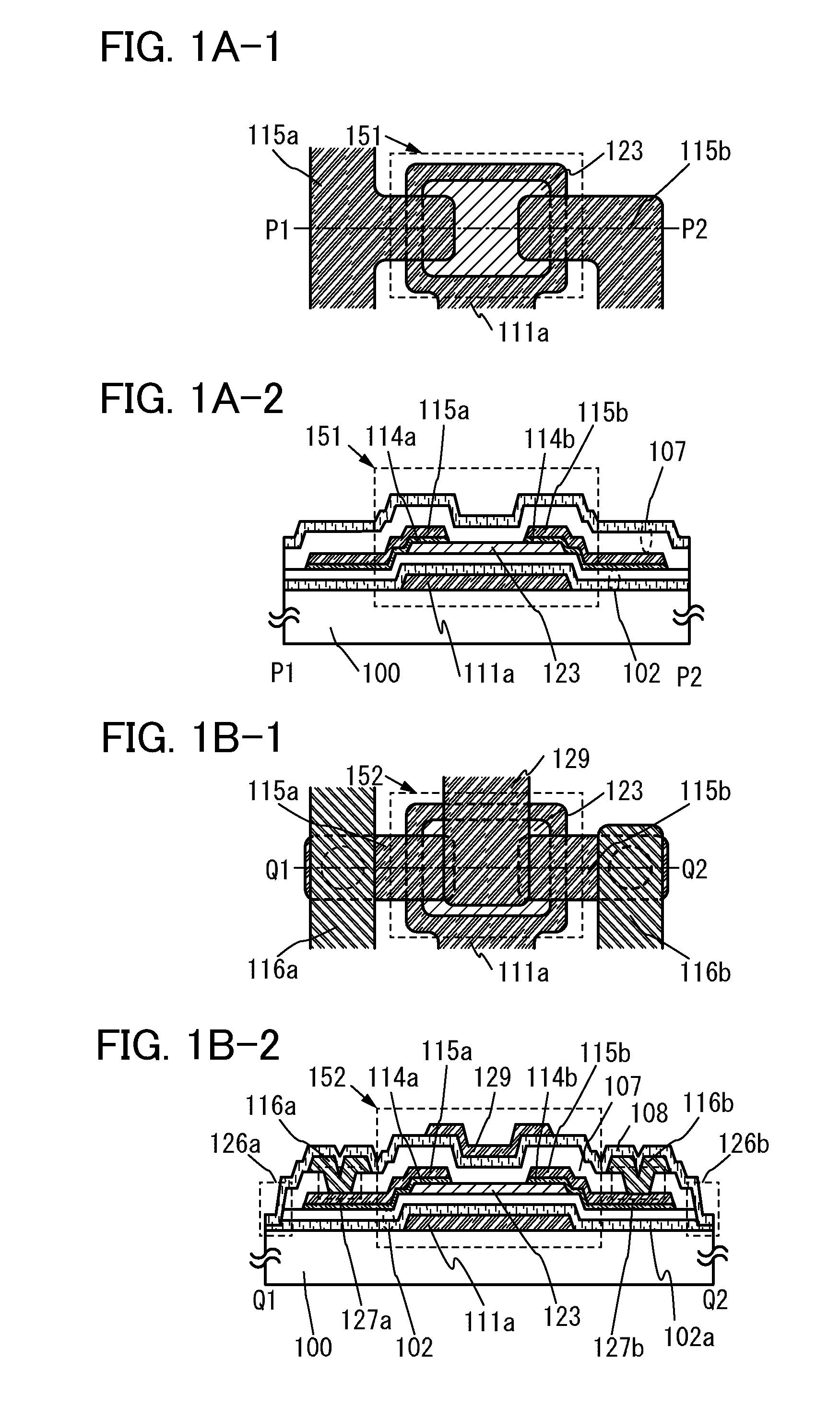
Semiconductor device and manufacturing method thereof
PatentActiveUS20110140109A1
Innovation
- A semiconductor device structure is implemented with a wide band gap oxide semiconductor layer and oxide conductive layers containing hydrogen and oxygen vacancies, where barrier layers prevent the diffusion of hydrogen and oxygen, ensuring low carrier concentration and high conductivity while maintaining light-transmitting properties.
Semiconductor device, method of manufacturing semiconductor device, photodiode array, and imaging apparatus
PatentActiveUS20160322416A1
Innovation
- A semiconductor device structure is implemented with an oxide semiconductor layer and a hydrogenated amorphous silicon photodiode, where a protective film is configured with an opening portion above the channel region of the oxide semiconductor layer, allowing for post-processing to enhance semiconductor characteristics and reduce hydrogen penetration, thereby stabilizing the threshold and improving reliability.
Material Composition Effects on Transport Properties
The composition of oxide semiconductors fundamentally determines their electron transport properties through several key mechanisms. In metal oxide semiconductors such as IGZO (Indium Gallium Zinc Oxide), ZnO, and SnO2, the metal-to-oxygen ratio significantly influences the band structure and carrier concentration. Higher oxygen vacancy concentrations typically result in increased carrier density, as each vacancy can donate up to two electrons to the conduction band, directly affecting conductivity.
The cation composition in multi-component oxide semiconductors creates unique transport characteristics. For instance, in IGZO, the incorporation of gallium stabilizes the amorphous structure while suppressing oxygen vacancy formation, resulting in enhanced carrier mobility compared to binary oxides. The indium content primarily determines the conduction band minimum energy level, with higher indium concentrations generally leading to improved electron transport properties due to the favorable overlap of In 5s orbitals.
Dopant incorporation represents another critical compositional factor affecting transport mechanisms. Intentional doping with elements such as aluminum in ZnO or antimony in SnO2 can dramatically alter carrier concentration and mobility. These dopants modify the electronic structure by introducing shallow donor states or altering the effective mass of charge carriers, thereby enhancing conductivity while potentially maintaining optical transparency.
The stoichiometry between metal and oxygen components directly impacts the formation of subgap states that can act as electron traps or generation-recombination centers. Non-stoichiometric compositions often exhibit higher conductivity but suffer from increased trap-assisted scattering, which degrades carrier mobility. This trade-off between carrier concentration and mobility represents a fundamental challenge in oxide semiconductor engineering.
Grain boundary composition in polycrystalline oxide semiconductors significantly affects inter-grain transport. The chemical nature of these boundaries, often enriched with specific elements or oxygen vacancies, creates potential barriers that electrons must overcome. Modifying the composition at grain boundaries through targeted doping or processing conditions can reduce these barriers, enhancing overall electron transport across the material.
Recent research has demonstrated that controlled introduction of secondary phases or compositional gradients can create beneficial heterojunctions within the oxide semiconductor, facilitating improved carrier transport through band engineering. These compositional strategies enable the development of oxide semiconductors with tailored transport properties for specific applications ranging from thin-film transistors to transparent conductive electrodes.
Environmental Stability and Degradation Mechanisms
Environmental stability represents a critical challenge for oxide semiconductor technologies, particularly in applications requiring long-term reliability. Oxide semiconductors, while offering numerous advantages in electron transport mechanisms, exhibit vulnerability to environmental factors that can significantly alter their performance characteristics over time. Atmospheric moisture, oxygen, and temperature fluctuations can trigger chemical and structural changes at the surface and bulk of these materials, directly impacting electron mobility and concentration.
The primary degradation pathway involves the adsorption of ambient gases, particularly water vapor and oxygen, onto the oxide semiconductor surface. These species can diffuse into the material structure, creating additional trap states that impede electron transport. In amorphous InGaZnO (a-IGZO) systems, for example, water molecules can form hydroxyl groups at metal cation sites, introducing acceptor-like states that deplete the conduction band of electrons and shift threshold voltages.
Prolonged exposure to ultraviolet radiation presents another significant degradation vector. UV photons generate electron-hole pairs that can facilitate photochemical reactions at the semiconductor surface, permanently altering the material's electronic structure. This phenomenon, known as persistent photoconductivity (PPC), manifests as continued conductivity changes even after illumination ceases, complicating device stability in applications with variable lighting conditions.
Temperature-induced degradation mechanisms also play a crucial role in oxide semiconductor reliability. Elevated temperatures accelerate diffusion processes of both intrinsic defects and extrinsic contaminants, potentially causing irreversible changes to the material's nanostructure. In zinc oxide-based systems, thermal stress can promote oxygen vacancy migration, creating conductive filaments that fundamentally alter electron transport pathways and device characteristics.
Bias stress effects represent perhaps the most operationally relevant degradation mechanism. Under prolonged gate bias, charge carriers can become trapped at the semiconductor-dielectric interface or within the dielectric itself, causing threshold voltage shifts and mobility degradation. This effect is particularly pronounced in oxide semiconductors with high defect densities or poorly optimized interfaces.
Mitigation strategies have evolved significantly, including passivation layers that serve as diffusion barriers against atmospheric contaminants, defect engineering to reduce trap state density, and compositional optimization to enhance inherent stability. Advanced encapsulation technologies using atomic layer deposition have demonstrated particular promise in creating hermetic barriers that preserve the intrinsic electron transport properties of oxide semiconductors across diverse environmental conditions.
Unlock deeper insights with Patsnap Eureka Quick Research — get a full tech report to explore trends and direct your research. Try now!
Generate Your Research Report Instantly with AI Agent
Supercharge your innovation with Patsnap Eureka AI Agent Platform!