How Oxide Semiconductor Improves Carrier Mobility in Thin-Film Transistors
SEP 25, 20259 MIN READ
Generate Your Research Report Instantly with AI Agent
Patsnap Eureka helps you evaluate technical feasibility & market potential.
Oxide Semiconductor Evolution and Objectives
Oxide semiconductor technology has undergone significant evolution since its inception in the early 2000s. The journey began with the discovery of amorphous oxide semiconductors (AOS) by Hosono's group in Japan, particularly the a-IGZO (amorphous indium gallium zinc oxide) which demonstrated unprecedented electron mobility compared to traditional amorphous silicon. This breakthrough marked the beginning of a new era in thin-film transistor (TFT) technology, offering a promising alternative to conventional silicon-based semiconductors.
The evolution of oxide semiconductors has been characterized by continuous improvements in material composition and processing techniques. Initially, the focus was on indium-based oxides due to their superior electron transport properties. However, concerns regarding indium scarcity prompted research into alternative materials such as zinc tin oxide (ZTO) and aluminum zinc oxide (AZO). Each iteration has contributed to enhancing carrier mobility while addressing challenges related to stability, uniformity, and manufacturing scalability.
A significant milestone in oxide semiconductor development was the transition from vacuum-based deposition methods to solution-processing techniques. This shift has enabled cost-effective, large-area fabrication, making oxide semiconductors increasingly attractive for commercial applications. The ability to process these materials at relatively low temperatures has further expanded their compatibility with flexible substrates, opening new avenues for flexible and transparent electronics.
The primary objective of oxide semiconductor research has been to maximize carrier mobility while maintaining other essential properties such as transparency, stability, and uniformity. Carrier mobility directly influences switching speed and power efficiency in TFTs, making it a critical parameter for high-performance electronic devices. Current research aims to achieve mobility values exceeding 50 cm²/Vs in amorphous oxide semiconductors, approaching the performance of polycrystalline silicon while retaining the advantages of amorphous materials.
Another key objective is to develop ambipolar oxide semiconductors that can efficiently transport both electrons and holes. Current oxide semiconductors predominantly exhibit n-type behavior, limiting their application in complementary circuits. Achieving balanced electron and hole transport would enable more efficient and versatile electronic systems, particularly for logic applications and integrated circuits.
Looking forward, the field is moving toward environmentally friendly, earth-abundant oxide semiconductors that maintain high performance while reducing reliance on rare or toxic elements. Additionally, there is growing interest in oxide semiconductors for emerging applications such as neuromorphic computing, where their unique properties can be leveraged to create brain-inspired electronic systems with adaptive functionality and low power consumption.
Market Demand for High-Mobility TFT Technologies
The global market for high-mobility thin-film transistor (TFT) technologies has experienced significant growth in recent years, driven primarily by the expanding display industry and emerging applications in flexible electronics. The demand for oxide semiconductor-based TFTs, particularly those utilizing indium gallium zinc oxide (IGZO), has surged due to their superior performance characteristics compared to conventional amorphous silicon (a-Si) TFTs.
Display manufacturers are increasingly seeking TFT technologies that can deliver higher refresh rates, improved resolution, and reduced power consumption. This demand is particularly evident in the premium smartphone and television segments, where consumers expect exceptional visual experiences. Market research indicates that the global display market reached approximately $140 billion in 2022, with high-performance TFT technologies representing a growing percentage of this value.
The shift toward flexible and foldable displays has further accelerated the need for high-mobility TFT solutions. Traditional a-Si TFTs, with carrier mobilities typically below 1 cm²/Vs, cannot adequately support these advanced display formats. In contrast, oxide semiconductor TFTs offer mobilities ranging from 10-50 cm²/Vs, making them ideal candidates for next-generation display applications.
Beyond consumer electronics, emerging sectors such as automotive displays, medical imaging, and industrial touchscreens are creating new market opportunities for high-mobility TFT technologies. The automotive display market alone is projected to grow at a compound annual growth rate of 8.5% through 2027, driven by increasing integration of digital cockpits and infotainment systems in vehicles.
Energy efficiency has become another critical market driver. As consumers and regulatory bodies place greater emphasis on sustainable technologies, the lower power consumption of oxide semiconductor TFTs compared to a-Si alternatives has become a significant selling point. This advantage is particularly valuable in battery-powered devices where extended operation time is a key competitive differentiator.
Regional analysis reveals that East Asia continues to dominate both the production and consumption of high-mobility TFT technologies, with China, South Korea, and Japan leading manufacturing capacity. However, North America and Europe represent substantial markets for end products incorporating these advanced display technologies.
Industry forecasts suggest that the market for oxide semiconductor TFTs will continue to expand as new applications emerge. The growing interest in transparent electronics, large-area sensors, and Internet of Things (IoT) devices presents additional growth vectors for high-mobility TFT technologies beyond traditional display applications.
Current Challenges in Oxide Semiconductor TFTs
Despite significant advancements in oxide semiconductor technology for thin-film transistors (TFTs), several critical challenges persist that limit their widespread adoption and performance optimization. One of the primary obstacles remains the trade-off between carrier mobility and stability. While amorphous oxide semiconductors like IGZO (Indium Gallium Zinc Oxide) offer improved mobility compared to a-Si:H, they still fall short of crystalline silicon performance, particularly when subjected to electrical stress or environmental factors.
The presence of oxygen vacancies, while beneficial for carrier generation, creates instability issues under bias stress conditions. These vacancies can migrate under electric fields, causing threshold voltage shifts and degrading device performance over time. This phenomenon is particularly problematic in display applications requiring long-term stability and consistent performance characteristics.
Manufacturing scalability presents another significant challenge. Current deposition techniques for high-quality oxide semiconductor films, such as pulsed laser deposition or sputtering, face difficulties in achieving uniform electrical properties across large substrates. The industry struggles to maintain consistent stoichiometry and minimize defect density during mass production, resulting in yield issues and performance variations between devices.
Interface quality between the oxide semiconductor and adjacent layers (gate dielectric, source/drain contacts) significantly impacts carrier transport. Poor interface quality leads to carrier trapping, scattering, and reduced effective mobility. Controlling these interfaces at the atomic level during manufacturing remains technically challenging, especially when implementing multi-component oxide systems.
Environmental sensitivity poses additional complications. Many oxide semiconductors exhibit performance degradation when exposed to moisture, oxygen, or light. This necessitates complex encapsulation solutions that add cost and manufacturing complexity while potentially limiting flexibility in certain applications.
The limited understanding of conduction mechanisms in multi-component oxide systems hinders systematic improvement approaches. Unlike crystalline silicon, where band transport dominates, carrier transport in oxide semiconductors involves complex percolation paths through metal s-orbitals, making predictive modeling and material optimization more challenging.
Cost considerations further complicate advancement, particularly regarding indium dependency. The reliance on indium, a relatively scarce element, raises sustainability concerns and price volatility risks. Research into indium-free alternatives has shown promise but typically results in reduced mobility or stability, creating difficult engineering trade-offs.
These challenges collectively represent significant barriers to fully realizing the potential of oxide semiconductor TFTs across various applications, from high-performance displays to flexible electronics and integrated circuits.
Current Approaches to Improve Carrier Mobility
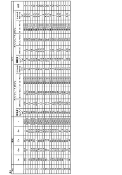
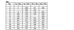
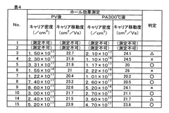
01 Material composition for improved carrier mobility
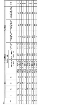
Various oxide semiconductor materials can be engineered to enhance carrier mobility in thin-film transistors. These include specific compositions of indium-gallium-zinc oxide (IGZO), indium-tin oxide, and other metal oxide combinations. The stoichiometric ratios of these elements significantly impact the electronic properties, with higher indium content often correlating with improved mobility. Post-deposition treatments and crystallinity control also play crucial roles in optimizing the semiconductor's electronic performance.- Material composition for enhanced carrier mobility: The choice of oxide semiconductor materials significantly impacts carrier mobility in thin-film transistors. Specific compositions such as indium-gallium-zinc oxide (IGZO), zinc tin oxide (ZTO), and indium zinc oxide (IZO) demonstrate superior electron mobility characteristics. The incorporation of certain dopants or the precise control of oxygen vacancies within these materials can further enhance carrier mobility properties, making them suitable for high-performance electronic applications.
- Fabrication techniques to improve mobility: Various fabrication methods can significantly enhance carrier mobility in oxide semiconductor TFTs. These include optimized annealing processes, controlled deposition parameters, and post-deposition treatments. Techniques such as plasma-enhanced deposition, pulsed laser deposition, and atomic layer deposition allow for precise control over film microstructure and interface quality. The processing temperature and atmosphere during fabrication also play crucial roles in determining the final carrier mobility characteristics.
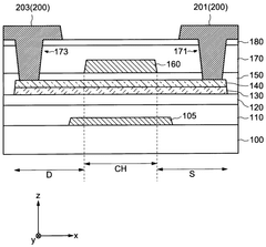
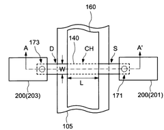
- Device structure optimization: The structural design of oxide semiconductor TFTs significantly influences carrier mobility. Various gate configurations (top-gate, bottom-gate, dual-gate), channel geometries, and electrode materials can be optimized to enhance carrier transport. The implementation of specific dielectric materials and interface engineering techniques reduces carrier scattering and trapping. Advanced structures such as multi-channel designs or heterojunction implementations further improve mobility characteristics for high-performance applications.
- Passivation and interface engineering: Interface quality between the oxide semiconductor and adjacent layers critically affects carrier mobility. Implementing effective passivation layers protects the semiconductor surface from environmental degradation and reduces interface trap states. Various passivation materials and techniques, including hydrogen incorporation, nitrogen treatment, or specific oxide capping layers, can significantly enhance mobility by reducing carrier scattering at interfaces. Controlling the formation of interface states through precise processing conditions further improves carrier transport properties.
- Stability and reliability enhancement: Maintaining high carrier mobility under various operational conditions is essential for practical applications. Techniques to enhance the stability of oxide semiconductor TFTs include stress compensation layers, bias stress mitigation strategies, and environmental protection methods. Addressing issues such as oxygen vacancy migration, hydrogen diffusion, and moisture sensitivity improves long-term reliability. Implementing specific buffer layers or compositional gradients within the device structure helps maintain consistent mobility characteristics throughout the operational lifetime.
02 Deposition techniques affecting mobility characteristics
The method of oxide semiconductor deposition significantly influences carrier mobility in the resulting thin-film transistors. Techniques such as sputtering, pulsed laser deposition, atomic layer deposition, and solution processing each produce films with different microstructures and defect densities. Process parameters including temperature, pressure, and gas composition during deposition directly impact the film quality. Optimized deposition conditions can reduce oxygen vacancies and other defects that act as scattering centers, thereby enhancing carrier mobility.Expand Specific Solutions03 Post-processing treatments to enhance mobility
Various post-deposition treatments can significantly improve carrier mobility in oxide semiconductor thin-film transistors. These include thermal annealing in different atmospheres (oxygen, nitrogen, forming gas), plasma treatments, and passivation layers. Such processes help reduce defects, optimize oxygen content, and improve the semiconductor-insulator interface quality. Specific annealing temperature profiles and durations are critical for achieving optimal electronic performance without degrading other device characteristics.Expand Specific Solutions04 Device structure optimization for mobility enhancement
The architecture of oxide semiconductor thin-film transistors significantly impacts carrier mobility. Key structural elements include gate dielectric material selection, electrode configurations, channel dimensions, and interface engineering. Bottom-gate vs. top-gate configurations offer different mobility advantages, while the choice of gate insulator material affects interface trap density. Novel structures such as dual-gate designs, recessed channels, or field-plate structures can further enhance carrier transport properties by optimizing electric field distribution within the device.Expand Specific Solutions05 Doping strategies to control carrier concentration and mobility
Strategic doping of oxide semiconductors can effectively modulate carrier concentration and mobility in thin-film transistors. Various dopants including hydrogen, nitrogen, metals (such as aluminum, titanium), and rare earth elements can be incorporated to control electronic properties. Co-doping approaches with multiple elements offer synergistic effects for mobility enhancement. The concentration and distribution of dopants must be precisely controlled to achieve optimal carrier transport while maintaining good stability and threshold voltage characteristics.Expand Specific Solutions
Leading Companies in Oxide Semiconductor Development
The oxide semiconductor market for thin-film transistors is currently in a growth phase, with increasing adoption driven by superior carrier mobility compared to traditional amorphous silicon. The global market is projected to reach significant scale as applications expand in display technologies and flexible electronics. Leading players include Semiconductor Energy Laboratory, which pioneered IGZO technology, alongside major display manufacturers like Samsung Display, LG Display, BOE Technology, and Japan Display who have commercialized oxide semiconductor TFTs. Research institutions such as University of Tokyo and Nara Institute of Science & Technology continue advancing fundamental understanding, while semiconductor manufacturers including SMIC and Intel are exploring integration possibilities. The technology has reached commercial maturity for display applications but remains in development for more advanced applications requiring higher mobility and stability.
Semiconductor Energy Laboratory Co., Ltd.
Technical Solution: Semiconductor Energy Laboratory (SEL) has pioneered oxide semiconductor technology with their CAAC (c-axis aligned crystalline) IGZO technology. Their approach involves creating highly crystalline oxide semiconductor films with improved carrier mobility exceeding 10 cm²/Vs, significantly higher than amorphous silicon. SEL's technology utilizes a unique deposition method that aligns the c-axis of IGZO crystals perpendicular to the substrate surface, creating ordered microstructure that reduces carrier scattering. They've developed proprietary sputtering techniques with precise oxygen partial pressure control during deposition, which minimizes oxygen vacancies that typically act as carrier traps. Additionally, SEL implements post-deposition annealing processes in controlled atmospheres to further optimize the semiconductor's electronic properties and stability.
Strengths: Industry-leading crystallinity control resulting in superior mobility; excellent stability against environmental stressors; low off-state leakage current. Weaknesses: More complex manufacturing process compared to conventional amorphous oxide semiconductors; requires specialized deposition equipment; higher production costs than standard a-Si TFTs.
Japan Display, Inc.
Technical Solution: Japan Display Inc. (JDI) has developed specialized oxide semiconductor technology focusing on high-mobility materials for advanced displays. Their approach centers on indium-gallium-zinc-oxide (IGZO) with proprietary modifications to the composition and structure. JDI employs a unique deposition method that creates a quasi-crystalline structure with improved short-range ordering compared to typical amorphous IGZO, resulting in reduced carrier scattering. Their technology incorporates carefully controlled hydrogen incorporation during deposition, which passivates oxygen vacancies and other defects that typically impede carrier movement. JDI has also developed specialized interface engineering techniques that minimize carrier trapping at the semiconductor-insulator boundary. Their manufacturing process includes precise control of oxygen partial pressure during sputtering and post-deposition treatments that optimize the semiconductor's electronic structure while maintaining process compatibility with existing manufacturing lines.
Strengths: Excellent balance between high mobility and manufacturing practicality; good stability under operational conditions; compatibility with both LCD and OLED display technologies. Weaknesses: Requires precise control of multiple process parameters; more sensitive to environmental contamination during manufacturing than conventional technologies; faces challenges with scaling to the highest mobility values reported in research settings.
Key Innovations in Oxide Semiconductor Materials
Thin-film transistor and electronic device
PatentWO2024195629A1
Innovation
- A thin film transistor is designed with an oxide semiconductor layer having a novel polycrystalline structure, characterized by a bixbite crystal structure and a large crystal grain length, achieved through a specific manufacturing process involving a metal oxide layer and TEM-ED mapping to optimize crystal orientation and grain boundaries, resulting in improved field effect mobility.

Thin film transistor comprising oxide semiconductor layer
PatentWO2017145695A1
Innovation
- A thin film transistor with an oxide semiconductor layer composed of In, Ga, Zn, and Sn, where the atomic ratio of In:Ga:Zn:Sn is optimized, and post-annealing treatments are used to increase the number of OH groups, resulting in improved carrier mobility and optical stress resistance by forming stable metal-oxygen bonds.
Manufacturing Scalability and Cost Analysis
The manufacturing scalability of oxide semiconductor thin-film transistors (TFTs) represents a significant advantage over traditional silicon-based technologies. Oxide semiconductors, particularly indium-gallium-zinc oxide (IGZO), can be deposited using conventional physical vapor deposition methods such as sputtering at relatively low temperatures (typically below 300°C). This compatibility with existing manufacturing infrastructure enables seamless integration into established production lines without requiring substantial capital investment in new equipment.
Cost analysis reveals that oxide semiconductor TFTs offer compelling economic benefits across the production chain. The raw material costs, while including relatively expensive elements like indium, remain competitive due to the extremely thin films required—typically in the range of 30-50 nm. This minimal material usage translates to significant cost savings compared to silicon-based alternatives that require more complex processing steps and thicker active layers.
The low-temperature processing capability of oxide semiconductors further reduces manufacturing costs by eliminating the need for expensive high-temperature annealing steps. This characteristic also enables compatibility with flexible substrates such as polyimide or PET, opening new market opportunities in flexible electronics while maintaining cost efficiency. Energy consumption during manufacturing is substantially lower than for polysilicon TFTs, contributing to both economic and environmental sustainability.
Yield rates for oxide semiconductor TFTs have steadily improved, now reaching industrial standards exceeding 95% in optimized production environments. This high yield is attributable to the amorphous nature of these materials, which provides greater tolerance to process variations and reduces defect sensitivity compared to crystalline alternatives. The resulting reduction in scrap rates directly impacts the final unit cost of devices incorporating these TFTs.
Scale economies are particularly favorable for oxide semiconductor technologies. As production volumes increase, the cost per unit decreases more rapidly than for competing technologies due to the relatively simple process flow and high throughput potential. Industry analysis indicates that at high-volume production, oxide semiconductor TFTs can achieve 30-40% cost reduction compared to LTPS (Low-Temperature Polysilicon) alternatives.
The supply chain for oxide semiconductor materials has matured significantly in recent years, with multiple suppliers now providing high-purity precursors and targets. This competition has stabilized prices and reduced supply risks, though concerns remain regarding indium availability for long-term, large-scale production. Several manufacturers are exploring indium-free alternatives such as zinc-tin oxide to mitigate these supply chain vulnerabilities while maintaining the carrier mobility advantages that make oxide semiconductors attractive.
Display Industry Integration Roadmap
The integration of oxide semiconductor technology into the display industry represents a significant technological evolution that is reshaping manufacturing processes and product capabilities. The display industry roadmap increasingly prioritizes oxide semiconductors, particularly indium gallium zinc oxide (IGZO) and related materials, as they enable higher resolution, lower power consumption, and improved performance in various display applications.
Major display manufacturers have established clear timelines for transitioning from conventional amorphous silicon (a-Si) to oxide semiconductor-based thin-film transistors (TFTs). This transition is occurring in phases, with high-end products adopting the technology first, followed by mid-range and eventually mainstream consumer displays. Industry projections indicate that by 2025, oxide semiconductors will dominate the premium display segment, with broader market penetration expected by 2028.
The fabrication infrastructure is evolving in parallel, with significant investments in production facilities capable of handling oxide semiconductor deposition and processing. Equipment manufacturers are developing specialized tools for uniform large-area deposition, precise patterning, and controlled annealing processes that are critical for optimizing carrier mobility in oxide semiconductors.
Supply chain considerations are also central to the integration roadmap. The industry is addressing potential bottlenecks related to indium availability and developing alternative compositions that reduce dependence on scarce elements while maintaining performance advantages. Vertical integration strategies are being implemented by major manufacturers to secure material supplies and specialized processing capabilities.
Standards organizations are working to establish unified specifications for oxide semiconductor performance metrics, testing protocols, and reliability requirements. These standardization efforts are crucial for ensuring consistency across the industry and facilitating broader adoption of the technology in diverse applications beyond traditional displays.
The roadmap also highlights the convergence of oxide semiconductor technology with other emerging display technologies, including micro-LED, quantum dot displays, and flexible/stretchable form factors. This convergence is creating new integration challenges but also opportunities for novel device architectures that leverage the unique properties of oxide semiconductors.
Environmental considerations are increasingly influencing the integration timeline, with manufacturers developing more sustainable production methods and exploring oxide semiconductor compositions with reduced environmental impact. This includes low-temperature processing techniques that decrease energy consumption during manufacturing and end-of-life recycling strategies for recovering valuable materials.
Unlock deeper insights with Patsnap Eureka Quick Research — get a full tech report to explore trends and direct your research. Try now!
Generate Your Research Report Instantly with AI Agent
Supercharge your innovation with Patsnap Eureka AI Agent Platform!