Oxide Semiconductor Application in UV and Visible Photodetectors
SEP 25, 20259 MIN READ
Generate Your Research Report Instantly with AI Agent
Patsnap Eureka helps you evaluate technical feasibility & market potential.
Oxide Semiconductor Photodetection Background and Objectives
Oxide semiconductors have emerged as promising materials for photodetection applications due to their unique electronic properties, wide bandgap tunability, and excellent optical transparency. The evolution of these materials can be traced back to the early 2000s when transparent conducting oxides (TCOs) like indium tin oxide (ITO) were primarily used as passive components in optoelectronic devices. The paradigm shifted significantly with the discovery of high-performance oxide semiconductor thin-film transistors, particularly those based on zinc oxide (ZnO) and its derivatives.
The technological trajectory has been marked by continuous improvements in material synthesis techniques, from conventional sputtering methods to advanced atomic layer deposition (ALD) and solution-processing approaches. These advancements have enabled precise control over the composition, stoichiometry, and defect states of oxide semiconductors, which are critical parameters for photodetection performance. The field has witnessed a transition from binary oxides (ZnO, SnO2) to more complex ternary and quaternary systems (InGaZnO, ZnSnO) that offer enhanced tunability of optoelectronic properties.
Recent years have seen increasing interest in oxide semiconductor photodetectors operating in the ultraviolet (UV) and visible spectral regions. This interest stems from their potential applications in environmental monitoring, biological sensing, security systems, and communication technologies. The inherent wide bandgap of many oxide semiconductors makes them naturally selective to UV radiation, addressing a significant technological gap in the photodetection spectrum where silicon-based devices show limited performance.
The research objectives in this field are multifaceted and ambitious. Primary goals include enhancing the responsivity and detectivity of oxide semiconductor photodetectors while maintaining their inherent advantages of transparency and stability. Researchers aim to extend the spectral response from the UV into the visible region through bandgap engineering, defect management, and heterojunction design. This would enable more versatile detection capabilities across a broader wavelength range.
Another critical objective is to improve the response speed of oxide semiconductor photodetectors, which has traditionally been limited by persistent photoconductivity effects and slow carrier dynamics. Strategies to address this challenge include interface engineering, novel device architectures, and hybrid material integration. Additionally, there is a growing emphasis on developing flexible and stretchable photodetectors to meet the demands of wearable electronics and Internet of Things (IoT) applications.
The ultimate technological goal is to establish oxide semiconductors as a viable alternative to conventional semiconductor materials in specific photodetection applications, particularly where transparency, UV sensitivity, and environmental stability are paramount. This requires not only advances in fundamental material science but also innovations in device design and manufacturing processes to ensure cost-effectiveness and scalability.
Market Analysis for UV-Visible Photodetector Applications
The global market for UV-visible photodetectors is experiencing robust growth, driven by increasing applications across multiple industries. The current market size is estimated at approximately 2.5 billion USD, with projections indicating a compound annual growth rate of 8.7% through 2028. This growth trajectory is supported by expanding applications in environmental monitoring, biomedical diagnostics, industrial quality control, and consumer electronics.
The healthcare and biomedical sector represents the largest market segment, accounting for nearly 30% of the total market share. Within this sector, oxide semiconductor-based photodetectors are gaining significant traction due to their superior performance in medical imaging, UV therapy monitoring, and point-of-care diagnostic devices. The ability of these devices to detect both UV and visible light makes them particularly valuable for applications requiring broad spectral response.
Industrial applications constitute the second-largest market segment, with approximately 25% market share. Manufacturing quality control, material analysis, and process monitoring systems increasingly rely on high-performance photodetectors. The automotive industry is also emerging as a significant consumer, incorporating these devices into advanced driver assistance systems and environmental sensors.
Consumer electronics represents a rapidly growing segment, particularly with the integration of photodetectors in smartphones, wearable devices, and smart home systems. This segment is expected to show the highest growth rate at 12.3% annually, driven by increasing consumer demand for devices with enhanced sensing capabilities.
Geographically, North America currently leads the market with approximately 35% share, followed by Europe (28%) and Asia-Pacific (25%). However, the Asia-Pacific region is expected to witness the fastest growth due to expanding manufacturing capabilities, increasing R&D investments, and growing adoption of advanced technologies in countries like China, Japan, and South Korea.
The market is characterized by varying requirements across different application segments. While consumer electronics prioritize miniaturization and cost-effectiveness, industrial and healthcare applications emphasize performance metrics such as sensitivity, response time, and reliability. This diversity in requirements is driving the development of specialized oxide semiconductor photodetectors tailored to specific application needs.
Key market drivers include increasing awareness of UV radiation hazards, growing demand for non-invasive medical diagnostics, stringent environmental monitoring regulations, and the expanding Internet of Things (IoT) ecosystem. These factors collectively contribute to the sustained market growth for oxide semiconductor-based UV and visible photodetectors across global markets.
Current Status and Technical Barriers in Oxide Semiconductor Photodetectors
Oxide semiconductor photodetectors have gained significant attention in recent years due to their unique properties and potential applications in UV and visible light detection. Currently, the field is dominated by several key materials including ZnO, TiO2, SnO2, In2O3, and Ga2O3, each offering distinct advantages for specific detection wavelengths and applications.
The global research landscape shows that Asia, particularly China, Japan, and South Korea, leads in oxide semiconductor photodetector development, with substantial contributions also coming from North America and Europe. Research institutions and companies in these regions have established strong patent portfolios and publication records in this domain.
Despite promising advancements, several technical barriers persist in oxide semiconductor photodetectors. The most significant challenge remains the trade-off between responsivity and response speed. High-performance devices often exhibit either excellent responsivity with slow response times or fast response with limited sensitivity, hindering their practical application in real-time monitoring systems.
Defect engineering represents another major hurdle. Native defects in oxide semiconductors, such as oxygen vacancies and metal interstitials, create unintended sub-bandgap states that affect device performance through persistent photoconductivity effects. These defects lead to long recovery times after light exposure, limiting the detectors' practical utility in applications requiring rapid cycling.
Stability issues under various environmental conditions pose additional challenges. Many oxide semiconductor photodetectors show performance degradation when exposed to humidity, temperature fluctuations, or prolonged operation. This instability stems from surface reactions with atmospheric species and structural changes within the material over time.
Fabrication consistency presents another barrier to commercialization. Current synthesis methods often produce materials with varying stoichiometry, crystallinity, and defect concentrations, resulting in device-to-device performance variations that complicate mass production and quality control.
The visible light detection capability of wide-bandgap oxide semiconductors remains limited without additional engineering. While naturally suited for UV detection, extending their sensitivity to the visible spectrum typically requires doping, heterostructure formation, or surface modification strategies that introduce complexity and potential performance compromises.
Integration challenges with existing semiconductor technologies also impede widespread adoption. Compatibility issues with silicon-based electronics, temperature constraints during processing, and interface quality control between oxide semiconductors and contact materials all present significant engineering challenges that must be overcome for practical device implementation.
Mainstream Oxide Material Solutions for UV-Visible Detection
01 Thin-film transistors using oxide semiconductors
Oxide semiconductors are widely used in thin-film transistors (TFTs) due to their excellent electrical properties, including high mobility and good stability. These materials enable the fabrication of transparent and flexible electronic devices. The oxide semiconductor layer typically consists of materials such as indium gallium zinc oxide (IGZO), which provides superior performance compared to conventional silicon-based semiconductors in certain applications.- Thin-film transistor applications of oxide semiconductors: Oxide semiconductors are widely used in thin-film transistors (TFTs) due to their excellent electrical properties, including high mobility and good stability. These materials enable the fabrication of transparent and flexible electronic devices with improved performance characteristics. The amorphous structure of certain oxide semiconductors allows for uniform electrical properties across large areas, making them suitable for display applications and other electronic devices.
- Fabrication methods for oxide semiconductor devices: Various fabrication techniques are employed to produce oxide semiconductor devices, including sputtering, chemical vapor deposition, and solution processing methods. These processes can be optimized to control the composition, crystallinity, and defect concentration in the oxide semiconductor layers. Post-deposition treatments such as annealing in different atmospheres can significantly improve the electrical properties and stability of the resulting devices.
- Material composition and doping of oxide semiconductors: The composition of oxide semiconductors can be tailored by incorporating various metal elements to achieve specific electrical and optical properties. Common oxide semiconductors include zinc oxide (ZnO), indium gallium zinc oxide (IGZO), and tin oxide (SnO2). Doping these materials with elements such as aluminum, gallium, or indium can modify their conductivity, carrier concentration, and band gap, enabling customization for specific applications.
- Sensing and detection applications of oxide semiconductors: Oxide semiconductors exhibit excellent gas sensing properties due to their surface reactivity with various gases, making them suitable for environmental monitoring and industrial safety applications. Their electrical properties change upon exposure to specific gases, allowing for the detection of pollutants, toxic gases, or volatile organic compounds. Additionally, oxide semiconductors can be used in biosensors, humidity sensors, and other detection devices due to their sensitivity to environmental changes.
- Memory and logic device applications of oxide semiconductors: Oxide semiconductors are increasingly being used in memory and logic devices due to their unique electrical properties and compatibility with existing semiconductor manufacturing processes. These materials can be incorporated into resistive random access memory (RRAM), ferroelectric field-effect transistors, and other emerging memory technologies. The ability to control the conductivity of oxide semiconductors through electric fields makes them promising candidates for low-power computing applications and neuromorphic systems.
02 Manufacturing processes for oxide semiconductor devices
Various manufacturing techniques are employed to produce oxide semiconductor devices, including sputtering, chemical vapor deposition, and solution processing methods. These processes control the composition, crystallinity, and defect concentration in the oxide semiconductor layer, which directly affects device performance. Post-deposition treatments such as annealing in specific atmospheres are often used to optimize the electrical properties of the oxide semiconductor films.Expand Specific Solutions03 Oxide semiconductor materials composition and properties
The composition of oxide semiconductor materials significantly influences their electrical and optical properties. Common oxide semiconductors include zinc oxide (ZnO), tin oxide (SnO2), indium oxide (In2O3), and multi-component oxides like IGZO. These materials exhibit wide bandgaps, high electron mobility, and optical transparency. Doping strategies are often employed to modify conductivity, carrier concentration, and stability of these materials for specific applications.Expand Specific Solutions04 Applications of oxide semiconductors in electronic devices
Oxide semiconductors are utilized in various electronic applications including display technologies, sensors, photovoltaics, and memory devices. Their unique combination of electrical conductivity and optical transparency makes them particularly valuable for transparent electronics. In display technologies, oxide semiconductor TFTs serve as pixel-driving elements in LCD and OLED displays, offering advantages such as high resolution and low power consumption.Expand Specific Solutions05 Stability and reliability improvements in oxide semiconductors
Enhancing the stability and reliability of oxide semiconductor devices is crucial for commercial applications. Various approaches include passivation layers, interface engineering, and compositional optimization to minimize defects and reduce threshold voltage shifts. Environmental factors such as humidity, temperature, and bias stress can degrade device performance over time, necessitating protective measures and robust device architectures to ensure long-term operational stability.Expand Specific Solutions
Leading Companies and Research Institutions in Oxide Semiconductor Field
The oxide semiconductor photodetector market is experiencing rapid growth, currently transitioning from early development to commercialization phase. The global market is expanding significantly due to increasing demand for high-performance UV and visible light detection across consumer electronics, healthcare, and environmental monitoring sectors. Technologically, the field shows varying maturity levels, with companies like Semiconductor Energy Laboratory, OSRAM Opto Semiconductors, and Seoul Viosys leading innovation in UV photodetection, while BOE Technology and Samsung SDI focus on visible spectrum applications. Research institutions including California Institute of Technology, ETRI, and NIMS are advancing fundamental materials science, creating a competitive ecosystem where industrial-academic partnerships drive commercialization. The market is characterized by strategic positioning between established semiconductor manufacturers and specialized optoelectronic companies developing proprietary oxide semiconductor technologies.
Semiconductor Energy Laboratory Co., Ltd.
Technical Solution: Semiconductor Energy Laboratory (SEL) has developed advanced oxide semiconductor photodetectors utilizing indium-gallium-zinc oxide (IGZO) thin-film technology. Their approach incorporates a unique multi-layer structure with optimized oxygen vacancy concentration to enhance UV and visible light detection sensitivity. SEL's photodetectors feature a bottom-gate thin-film transistor architecture with amorphous IGZO as the active layer, enabling high electron mobility (>10 cm²/Vs) while maintaining transparency in the visible spectrum[1]. The company has pioneered the integration of these photodetectors with readout circuitry on the same substrate, creating monolithic image sensors with high fill factors exceeding 70%. Their recent innovations include implementing bandgap engineering through compositional tuning of the oxide semiconductor layers to achieve wavelength selectivity between UV and visible regions[3], and developing self-powered photodetector arrays that generate photocurrent without external bias voltage.
Strengths: Superior integration capability with display and readout electronics; excellent stability under illumination stress; compatibility with large-area, low-temperature fabrication processes enabling flexible device applications. Weaknesses: Lower quantum efficiency compared to crystalline semiconductor alternatives; relatively slower response time in the millisecond range; challenges in achieving high sensitivity across the entire visible spectrum without additional filtering.
Electronics & Telecommunications Research Institute
Technical Solution: The Electronics & Telecommunications Research Institute (ETRI) has developed advanced oxide semiconductor photodetectors utilizing innovative material systems and device architectures. Their research focuses on amorphous oxide semiconductors (AOS) including indium-gallium-zinc oxide (IGZO), zinc-tin oxide (ZTO), and indium-zinc oxide (IZO) for both UV and visible light detection applications. ETRI's approach incorporates multilayer thin-film structures with engineered band alignments to optimize carrier generation, transport, and collection efficiency[6]. Their photodetectors feature a vertical architecture with transparent conducting oxide electrodes, enabling high optical transparency (>80%) in the visible region while maintaining excellent electrical conductivity. ETRI has pioneered the development of solution-processed oxide semiconductor photodetectors using novel sol-gel and hydrothermal synthesis methods, significantly reducing manufacturing costs while maintaining performance comparable to vacuum-deposited counterparts. Their recent innovations include the implementation of quantum dots and plasmonic nanostructures within the oxide semiconductor matrix to enhance light absorption and extend the spectral response range[8]. Additionally, ETRI has developed self-powered photodetectors based on oxide semiconductor heterojunctions that generate photocurrent without external bias, making them suitable for low-power IoT and environmental monitoring applications.
Strengths: Excellent compatibility with large-area electronics and display technologies; tunable spectral response through composition engineering; high stability under various environmental conditions; low-cost fabrication potential through solution processing. Weaknesses: Lower carrier mobility compared to crystalline counterparts limiting response speed; persistent photoconductivity effects in some material compositions; challenges in achieving uniform performance across large substrate areas.
Key Patents and Technical Innovations in Oxide Photodetectors
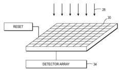
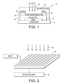
UV sensor with nonvolatile memory using oxide semiconductor films
PatentActiveUS9263124B2
Innovation
- A bottom gate architecture oxide semiconductor UV sensor with a reset mechanism, utilizing a transparent dielectric and conductive materials like indium zinc oxide, integrated into arrays for UV light detection, where the persistent photoconductivity is exploited for memory functionality and reset via positive gate bias or heating.
Oxide semiconductor device with oxide semiconductor layers of different oxygen concentrations and method of manufacturing the same
PatentInactiveUS8368067B2
Innovation
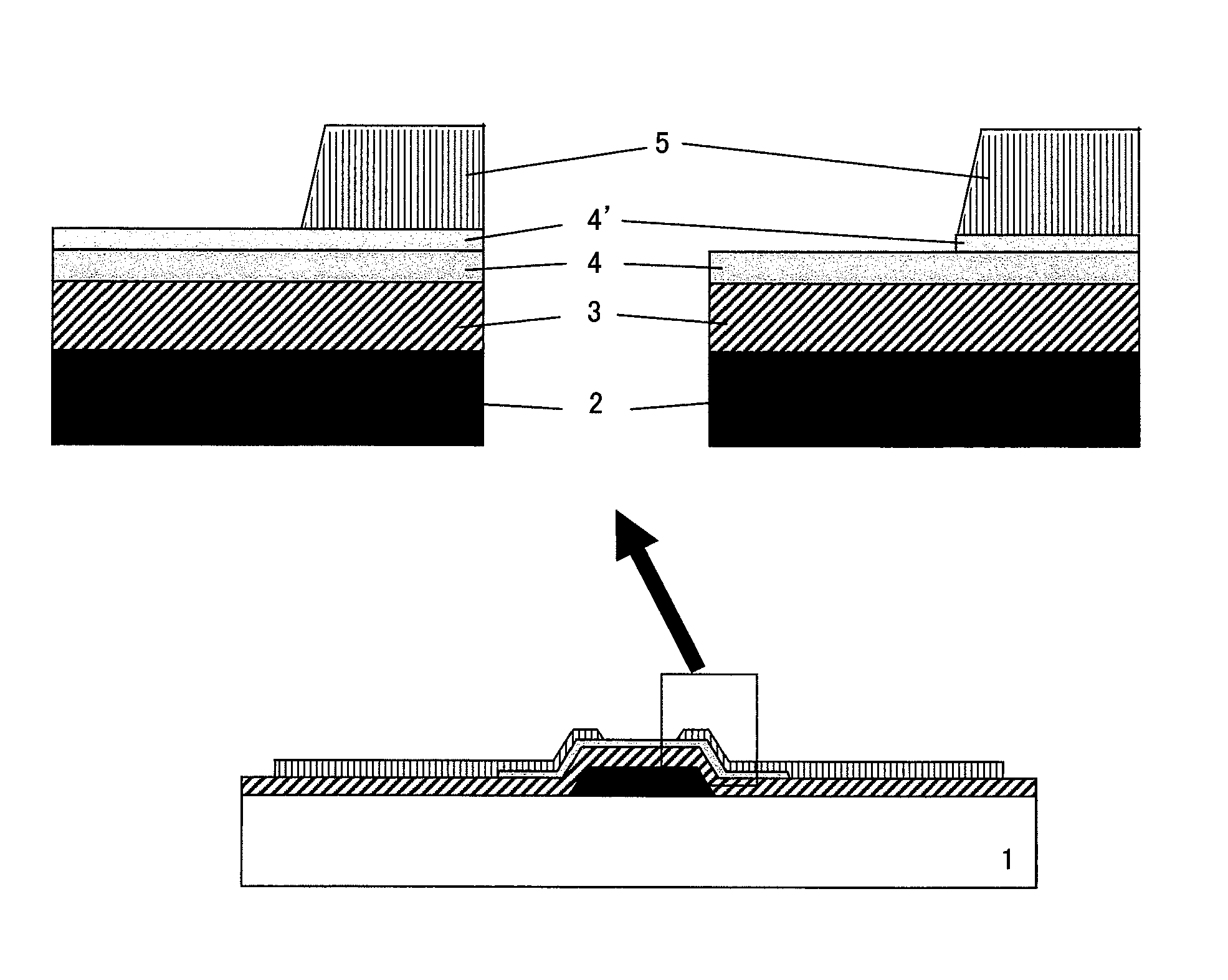
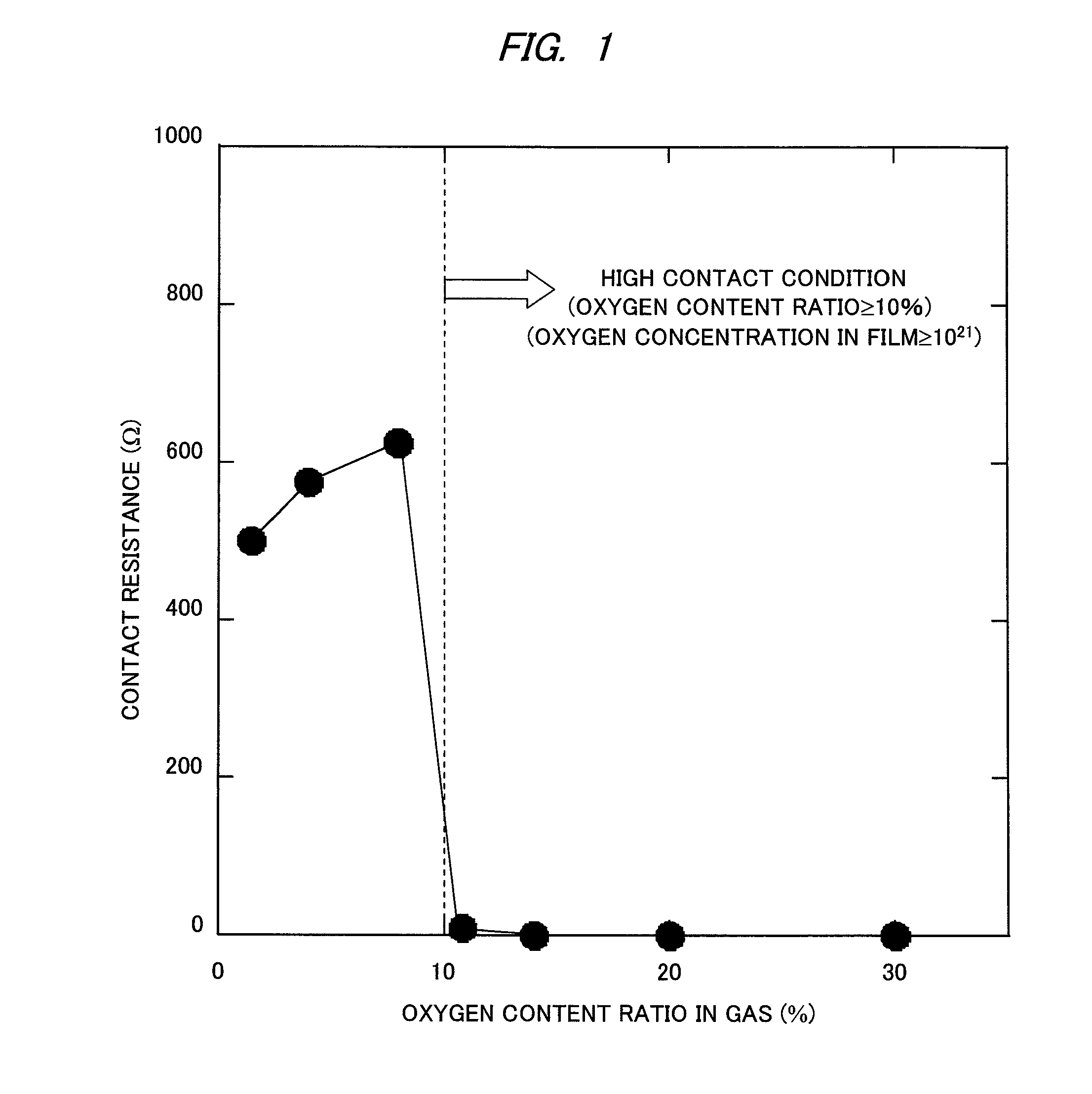
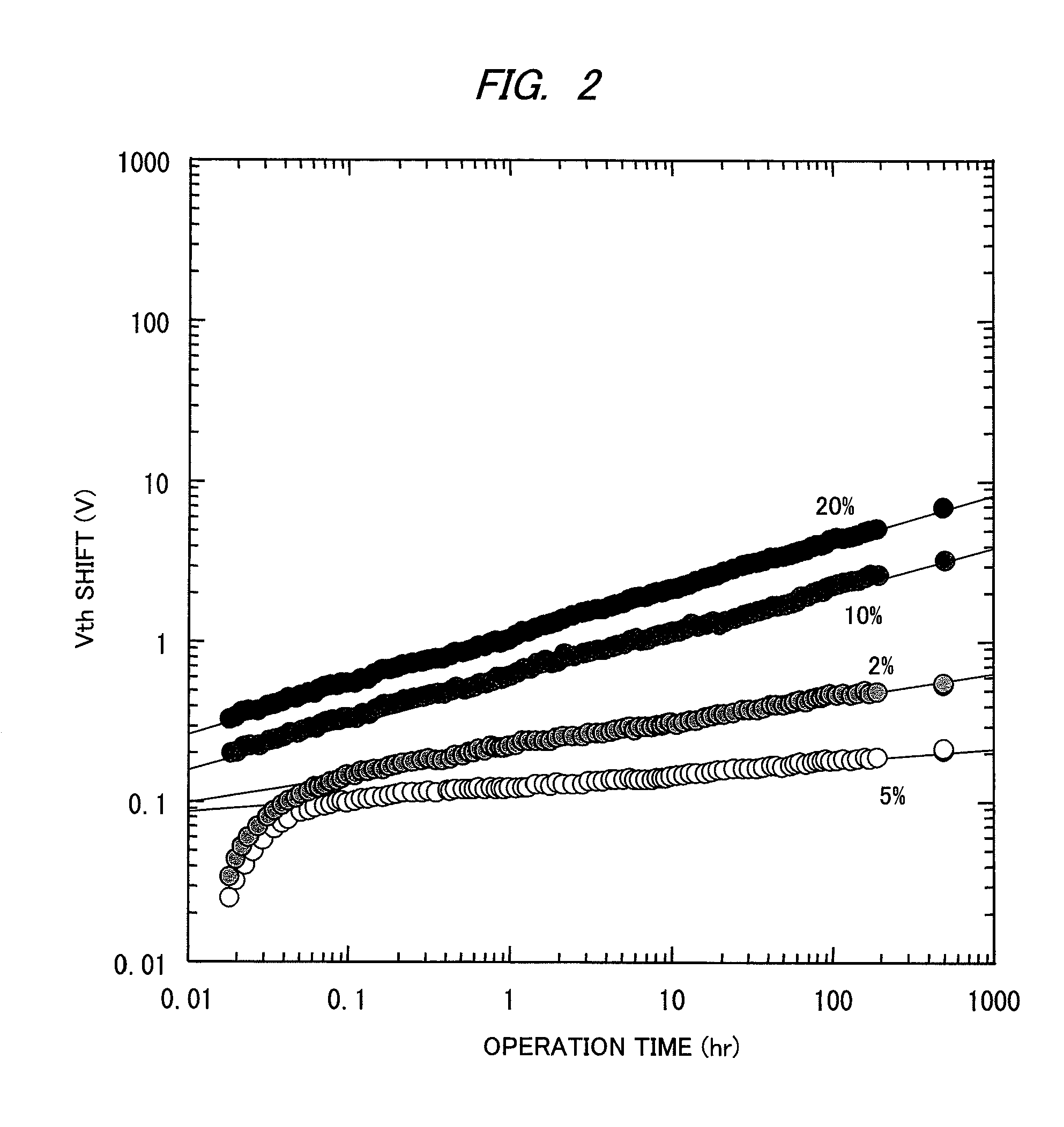
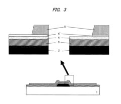
- A multilayered structure is implemented with an oxide semiconductor layer having a low oxygen content ratio near the gate insulating film and a high oxygen content ratio near the metal electrode, optimizing oxygen concentrations to balance contact resistance and threshold potential shift, ensuring effective ohmic contact and reliability.
Material Optimization Strategies for Spectral Selectivity
Spectral selectivity is a critical parameter for oxide semiconductor-based photodetectors, determining their ability to respond to specific wavelength ranges while rejecting others. Material optimization strategies for achieving precise spectral selectivity in UV and visible photodetectors involve several complementary approaches that can be tailored to specific application requirements.
Bandgap engineering represents the primary strategy for controlling spectral response in oxide semiconductors. By adjusting the composition of ternary and quaternary oxide systems such as ZnMgO, InGaZnO, or ZnSnO, researchers can precisely tune the bandgap energy to correspond with desired detection wavelengths. For instance, increasing the Mg content in ZnMgO systematically shifts the cutoff wavelength toward the UV region, enabling customized spectral windows.
Nanostructuring offers another powerful approach to enhance spectral selectivity. Quantum confinement effects in oxide nanostructures can modify the effective bandgap, while the geometry of nanowires, nanorods, and nanoparticles can be engineered to preferentially absorb specific wavelengths. Recent advances in controlled synthesis methods have enabled the fabrication of size-uniform oxide nanostructures with predictable spectral responses.
Surface modification techniques, including functionalization with organic molecules or plasmonic nanoparticles, provide additional mechanisms for spectral tuning. These surface treatments can introduce sub-bandgap states or localized surface plasmon resonance effects that enhance absorption at targeted wavelengths. For example, gold nanoparticle decoration on ZnO surfaces has demonstrated enhanced visible light response without compromising UV sensitivity.
Heterojunction engineering represents a sophisticated approach where multiple oxide semiconductors with different bandgaps are combined to create customized spectral responses. Type-II band alignments in particular can facilitate charge separation while enabling wavelength-selective detection. Notable examples include CuO/ZnO and NiO/TiO2 heterojunctions that exhibit enhanced visible light response.
Defect engineering has emerged as a promising strategy for introducing intermediate energy levels within the bandgap. Controlled introduction of oxygen vacancies, metal interstitials, or dopants can create sub-bandgap absorption bands that extend the spectral response into specific regions. However, this approach requires precise control over defect concentration and distribution to maintain detector performance metrics.
Recent advances in computational materials science have accelerated these optimization efforts through predictive modeling of electronic structures and optical properties. High-throughput screening methods combined with machine learning algorithms now enable rapid identification of promising oxide semiconductor compositions with tailored spectral selectivity for next-generation photodetector applications.
Environmental Impact and Sustainability of Oxide Semiconductor Manufacturing
The manufacturing processes of oxide semiconductors for photodetector applications present significant environmental considerations that must be addressed for sustainable development. Traditional semiconductor manufacturing often involves energy-intensive processes and hazardous materials, but oxide semiconductors offer several environmental advantages. Metal oxide materials such as ZnO, TiO2, and In2O3 generally require lower processing temperatures compared to silicon-based technologies, resulting in reduced energy consumption during fabrication.
However, certain oxide semiconductor manufacturing processes still utilize toxic precursors and solvents that pose environmental risks. For instance, indium-based compounds used in ITO (Indium Tin Oxide) production involve mining practices with substantial ecological footprints. The scarcity of indium also raises sustainability concerns regarding long-term supply chain viability for these materials.
Water consumption represents another critical environmental factor in oxide semiconductor production. Wet chemical methods commonly employed in synthesis require significant water resources and generate wastewater containing metal ions and chemical residues. Advanced water recycling systems and closed-loop manufacturing processes are being developed to mitigate these impacts, with some facilities reporting up to 80% reduction in water usage through implementation of such technologies.
Life cycle assessment (LCA) studies indicate that oxide semiconductor photodetectors generally have lower embodied energy compared to conventional silicon-based alternatives. This advantage becomes particularly pronounced when considering solution-processed oxide semiconductors, which can be manufactured using techniques like inkjet printing and spin coating that minimize material waste and energy requirements.
End-of-life management presents both challenges and opportunities for oxide semiconductor sustainability. While some metal oxides are potentially recoverable and recyclable, current infrastructure for reclaiming these materials from discarded photodetectors remains underdeveloped. Research into green chemistry approaches is advancing the development of environmentally benign synthesis routes using non-toxic precursors and bio-inspired processes.
Industry initiatives are increasingly focusing on replacing rare or toxic elements with earth-abundant alternatives. For example, aluminum-doped zinc oxide (AZO) and fluorine-doped tin oxide (FTO) are being explored as sustainable alternatives to ITO for transparent conducting oxide applications in photodetectors. These substitutions not only address resource scarcity concerns but often result in devices with comparable or enhanced performance characteristics.
Unlock deeper insights with Patsnap Eureka Quick Research — get a full tech report to explore trends and direct your research. Try now!
Generate Your Research Report Instantly with AI Agent
Supercharge your innovation with Patsnap Eureka AI Agent Platform!