Oxide Semiconductor Safety and Regulatory Guidelines for Electronics
SEP 25, 20259 MIN READ
Generate Your Research Report Instantly with AI Agent
Patsnap Eureka helps you evaluate technical feasibility & market potential.
Oxide Semiconductor Evolution and Safety Objectives
Oxide semiconductors have evolved significantly since their initial discovery in the early 20th century. The journey began with copper oxide semiconductors in the 1920s, followed by zinc oxide research in the 1950s. However, the field experienced a revolutionary transformation in 2004 when Hosono and colleagues demonstrated transparent amorphous oxide semiconductors (TAOS) with remarkable electron mobility. This breakthrough catalyzed intensive research and development, particularly in thin-film transistor (TFT) applications for display technologies.
The evolution of oxide semiconductors has been characterized by continuous improvements in material composition, deposition techniques, and device architectures. Indium gallium zinc oxide (IGZO) emerged as a dominant material due to its excellent electrical properties and stability. Recent years have witnessed the development of indium-free alternatives such as zinc tin oxide (ZTO) to address supply chain concerns related to indium scarcity.
As oxide semiconductors transition from research laboratories to mass production environments, safety considerations have become increasingly paramount. The primary safety objectives in this domain encompass several critical dimensions. First, ensuring occupational safety during manufacturing processes is essential, as the production often involves potentially hazardous materials and processes including high-temperature treatments and chemical etching.
Environmental safety represents another crucial objective, focusing on minimizing ecological impacts throughout the product lifecycle. This includes responsible sourcing of raw materials, reducing waste during manufacturing, and implementing effective end-of-life recycling strategies for oxide semiconductor components. The industry aims to develop comprehensive guidelines for proper disposal and recycling of devices containing these materials.
Consumer safety stands as a fundamental objective, particularly as oxide semiconductors find applications in wearable electronics and medical devices that maintain close contact with users. Understanding potential biocompatibility issues and long-term exposure effects has become a priority research area. The industry is working toward establishing standardized testing protocols to evaluate the safety of these materials in various application scenarios.
Regulatory compliance forms the fourth pillar of safety objectives. As oxide semiconductor technology matures, regulatory frameworks are evolving to address specific safety concerns. The industry aims to develop harmonized global standards that can facilitate international trade while ensuring consistent safety levels across different jurisdictions. This includes establishing clear guidelines for material characterization, risk assessment methodologies, and acceptable exposure limits.
The convergence of these safety objectives with technological advancement presents both challenges and opportunities. Future research directions will likely focus on developing inherently safer oxide semiconductor materials and processes while maintaining or enhancing performance characteristics.
Market Demand for Safe Oxide Semiconductor Electronics
The global market for oxide semiconductor-based electronics has witnessed substantial growth in recent years, driven primarily by increasing demand for high-performance, energy-efficient display technologies and power devices. Market research indicates that the oxide semiconductor market, particularly for indium gallium zinc oxide (IGZO) and related materials, is projected to grow at a compound annual growth rate of over 12% through 2028, reflecting strong industry confidence in these technologies.
Consumer electronics represents the largest application segment, with manufacturers increasingly adopting oxide semiconductor technologies in smartphones, tablets, and televisions to achieve higher resolution displays with lower power consumption. This trend is particularly evident in the premium device segment, where energy efficiency and display quality serve as key differentiators in a competitive marketplace.
The automotive sector has emerged as a rapidly expanding market for oxide semiconductor applications, particularly in advanced driver-assistance systems (ADAS) and infotainment displays. As vehicles become more electrified and autonomous, the demand for reliable, high-performance semiconductor components that can withstand harsh operating conditions continues to rise. Industry forecasts suggest that automotive applications of oxide semiconductors could grow at nearly 18% annually over the next five years.
Healthcare and medical device manufacturers are increasingly exploring oxide semiconductor technologies for wearable health monitors, medical imaging equipment, and implantable devices. The biocompatibility aspects of certain oxide materials make them particularly attractive for applications involving direct or indirect patient contact, creating a specialized market niche with stringent safety requirements.
Industrial automation and Internet of Things (IoT) applications represent another significant growth vector, with oxide semiconductors enabling more efficient sensors, control systems, and communication devices. The industrial sector particularly values the radiation hardness and temperature stability characteristics of many oxide semiconductor materials.
Market analysis reveals growing consumer and regulatory pressure for electronics manufacturers to demonstrate comprehensive safety compliance across their supply chains. This has created demand for standardized safety guidelines specific to oxide semiconductor technologies, as existing frameworks often fail to address the unique properties and potential hazards of these materials.
Regional market assessment shows Asia-Pacific dominating oxide semiconductor production, with Japan, South Korea, and Taiwan leading in technology development. However, significant market growth is occurring in North America and Europe, driven by applications in premium consumer electronics and specialized industrial systems where safety certifications carry substantial market value.
Current Safety Challenges in Oxide Semiconductor Technology
The oxide semiconductor industry faces several critical safety challenges that require immediate attention. The rapid adoption of these materials in consumer electronics, medical devices, and industrial applications has outpaced the development of comprehensive safety frameworks. Current regulatory guidelines remain fragmented across different regions, creating compliance difficulties for global manufacturers and potentially compromising user safety.
Material toxicity represents a significant concern, particularly regarding indium, gallium, and zinc compounds used in oxide semiconductors. Recent studies have identified potential health risks associated with nanoparticle exposure during manufacturing processes, with insufficient data on long-term occupational exposure effects. The industry lacks standardized protocols for handling these materials, especially during fabrication and disposal phases.
Electrical safety issues have emerged as oxide semiconductors increasingly power high-voltage applications. The unique electrical properties that make these materials valuable also create novel failure modes not adequately addressed by existing safety standards. Thermal runaway events, while rare, have been documented in devices utilizing certain oxide semiconductor configurations, highlighting the need for specialized testing methodologies.
Environmental contamination presents another challenge, as manufacturing byproducts contain potentially harmful compounds. Current waste management practices vary significantly across production facilities, with limited oversight regarding the disposal of chemical precursors and etching solutions. The environmental persistence of certain oxide compounds remains poorly understood, complicating risk assessment efforts.
Electromagnetic interference (EMI) characteristics of oxide semiconductor devices represent an evolving safety concern, particularly in medical and transportation applications. The industry lacks comprehensive testing standards to evaluate EMI susceptibility and emissions across the full operational range of these materials, creating potential safety vulnerabilities in critical systems.
Supply chain security has emerged as a safety consideration, with concerns about material authenticity and quality control. Counterfeit components incorporating substandard oxide semiconductors have been identified in various markets, potentially compromising device performance and safety. Traceability systems remain inadequate for ensuring material provenance throughout complex global supply networks.
Regulatory harmonization represents perhaps the most pressing challenge. Different jurisdictions have developed disparate approaches to oxide semiconductor safety, creating a complex compliance landscape. The European Union's emphasis on precautionary principles contrasts with more permissive frameworks in other regions, complicating global product development and potentially creating safety standard arbitrage opportunities that could undermine consumer protection.
Existing Safety Compliance Solutions
01 Safety regulations for oxide semiconductor manufacturing
Manufacturing processes for oxide semiconductors must adhere to specific safety guidelines to protect workers and the environment. These regulations cover handling of precursor materials, waste management, and exposure limits for potentially hazardous compounds used in production. Manufacturers must implement proper ventilation systems, personal protective equipment protocols, and regular monitoring of air quality in production facilities to ensure compliance with occupational health standards.- Safety regulations for oxide semiconductor manufacturing: Manufacturing processes for oxide semiconductors must adhere to specific safety guidelines to protect workers and the environment. These regulations cover handling of precursor materials, waste management, and exposure limits for potentially hazardous compounds used in the fabrication process. Proper ventilation systems, personal protective equipment, and emergency protocols are essential components of these safety frameworks to minimize health risks associated with chemical exposure during production.
- Environmental compliance for oxide semiconductor devices: Oxide semiconductor devices must meet environmental compliance standards throughout their lifecycle, from production to disposal. These guidelines address the reduction of harmful substances, energy efficiency requirements, and end-of-life management. Manufacturers must document material composition, ensure proper recycling protocols, and minimize environmental impact through sustainable practices. Compliance with international standards such as RoHS and REACH is mandatory for market access in many regions.
- Quality control and certification requirements: Oxide semiconductor products undergo rigorous quality control procedures and certification processes to ensure safety and reliability. These include standardized testing protocols for electrical performance, thermal stability, and mechanical durability. Third-party certification bodies verify compliance with industry standards and regulatory requirements. Documentation of testing methodologies, results, and quality management systems is essential for obtaining necessary certifications and maintaining market approval.
- Health risk assessment and mitigation strategies: Comprehensive health risk assessments are required for oxide semiconductor technologies to identify potential hazards and develop appropriate mitigation strategies. These assessments evaluate exposure pathways, toxicological profiles of materials, and potential long-term health effects. Risk mitigation includes engineering controls, administrative measures, and ongoing monitoring programs. Regular updates to safety data sheets and employee training programs ensure awareness of potential risks and proper handling procedures.
- Regulatory compliance monitoring and reporting: Organizations working with oxide semiconductors must implement systems for monitoring and reporting regulatory compliance. This includes tracking changes in applicable regulations across different jurisdictions, maintaining documentation of compliance activities, and submitting required reports to regulatory authorities. Digital compliance management systems help organizations stay current with evolving requirements and demonstrate due diligence through comprehensive record-keeping and timely reporting of safety incidents or compliance issues.
02 Environmental impact assessment of oxide semiconductor devices
Regulatory frameworks require environmental impact assessments for oxide semiconductor technologies throughout their lifecycle. These assessments evaluate resource consumption, energy efficiency, waste generation, and end-of-life disposal considerations. Manufacturers must document the environmental footprint of their oxide semiconductor products, including potential leaching of toxic materials, recyclability of components, and overall sustainability metrics to meet increasingly stringent global environmental standards.Expand Specific Solutions03 Compliance certification for oxide semiconductor applications
Oxide semiconductor devices require various compliance certifications before market entry, depending on their application and target region. These certifications verify adherence to electrical safety standards, electromagnetic compatibility requirements, and specific industry regulations. The certification process typically involves third-party testing, documentation of manufacturing processes, risk assessments, and regular audits to maintain compliance status as regulations evolve over time.Expand Specific Solutions04 Health risk assessment protocols for oxide semiconductors
Standardized protocols exist for assessing potential health risks associated with oxide semiconductor materials and devices. These protocols evaluate biocompatibility, potential toxicity through various exposure routes, and long-term health effects. Manufacturers must conduct appropriate testing based on the intended application, with more rigorous requirements for devices with direct human contact or those used in medical applications. Risk assessment data must be documented and made available to regulatory authorities.Expand Specific Solutions05 International standards harmonization for oxide semiconductors
Global efforts are underway to harmonize safety and regulatory standards for oxide semiconductor technologies across different regions. These initiatives aim to establish consistent testing methodologies, safety thresholds, and compliance requirements to facilitate international trade while maintaining high safety standards. Manufacturers must navigate complex regulatory landscapes that may include region-specific requirements while working toward compliance with internationally recognized standards and certification systems.Expand Specific Solutions
Key Industry Stakeholders and Regulatory Bodies
The oxide semiconductor safety and regulatory landscape is evolving within a maturing industry characterized by growing market demand for energy-efficient, high-performance electronics. Major players like Samsung Electronics, LG Display, and Taiwan Semiconductor Manufacturing Co. are driving technological advancements, while research institutions such as Semiconductor Energy Laboratory and North Carolina State University contribute to fundamental safety standards. The competitive environment includes specialized manufacturers like ROHM, Japan Display, and OSRAM Opto Semiconductors, who are developing proprietary safety protocols. As oxide semiconductor technology transitions from emerging to established status, regulatory frameworks are becoming more standardized, with companies increasingly focusing on environmental compliance and worker safety alongside performance improvements.
Semiconductor Energy Laboratory Co., Ltd.
Technical Solution: Semiconductor Energy Laboratory (SEL) has developed comprehensive safety protocols for oxide semiconductor manufacturing, focusing on indium gallium zinc oxide (IGZO) technology. Their approach includes rigorous material handling guidelines that address potential hazards associated with metal oxide precursors and processing chemicals. SEL has implemented advanced containment systems for volatile organic compounds (VOCs) released during deposition processes, reducing workplace exposure to below 1ppm for most compounds. Their safety framework incorporates specialized ventilation systems designed specifically for oxide semiconductor fabrication facilities, with redundant filtration to capture nanoparticulate matter. Additionally, SEL has pioneered waste management protocols for oxide semiconductor materials that comply with RoHS and REACH regulations, ensuring proper disposal of indium and gallium compounds that could pose environmental risks. The company regularly conducts toxicological assessments of their oxide semiconductor materials, with published studies demonstrating minimal bioaccumulation potential compared to traditional semiconductor materials.
Strengths: Industry-leading expertise in IGZO technology with extensive safety research data; comprehensive approach covering manufacturing, handling, and disposal; strong compliance with international regulations. Weaknesses: Safety protocols are primarily optimized for their proprietary manufacturing processes; implementation costs may be prohibitive for smaller manufacturers; some guidelines may be overly conservative, potentially limiting production efficiency.
LG Display Co., Ltd.
Technical Solution: LG Display has established a robust oxide semiconductor safety framework specifically tailored for large-scale production environments. Their approach centers on a three-tier safety system for oxide thin-film transistor (TFT) manufacturing that addresses chemical exposure, physical hazards, and environmental impact. For chemical safety, LG has developed specialized handling protocols for precursor materials like indium, gallium, and zinc compounds, implementing automated material transfer systems that minimize worker contact with potentially hazardous substances. Their facilities incorporate advanced air quality monitoring systems that continuously measure metal oxide particulate concentrations, maintaining levels below 0.05mg/m³ throughout production areas. LG Display has also pioneered thermal management systems for oxide semiconductor annealing processes, reducing fire and explosion risks associated with high-temperature processing. Their regulatory compliance program includes regular third-party verification of safety measures against standards including IEC 62368-1 for electronic equipment safety and various regional chemical regulations. LG has further developed specialized end-of-life recycling protocols for oxide semiconductor displays that recover over 90% of rare metals while preventing environmental contamination.
Strengths: Extensive real-world implementation in high-volume manufacturing environments; comprehensive monitoring systems with quantifiable safety metrics; strong integration with existing electronics industry safety standards. Weaknesses: Guidelines primarily focused on display applications rather than broader semiconductor uses; significant capital investment required for full implementation; some proprietary safety technologies not available to the broader industry.
Critical Safety Standards and Testing Protocols
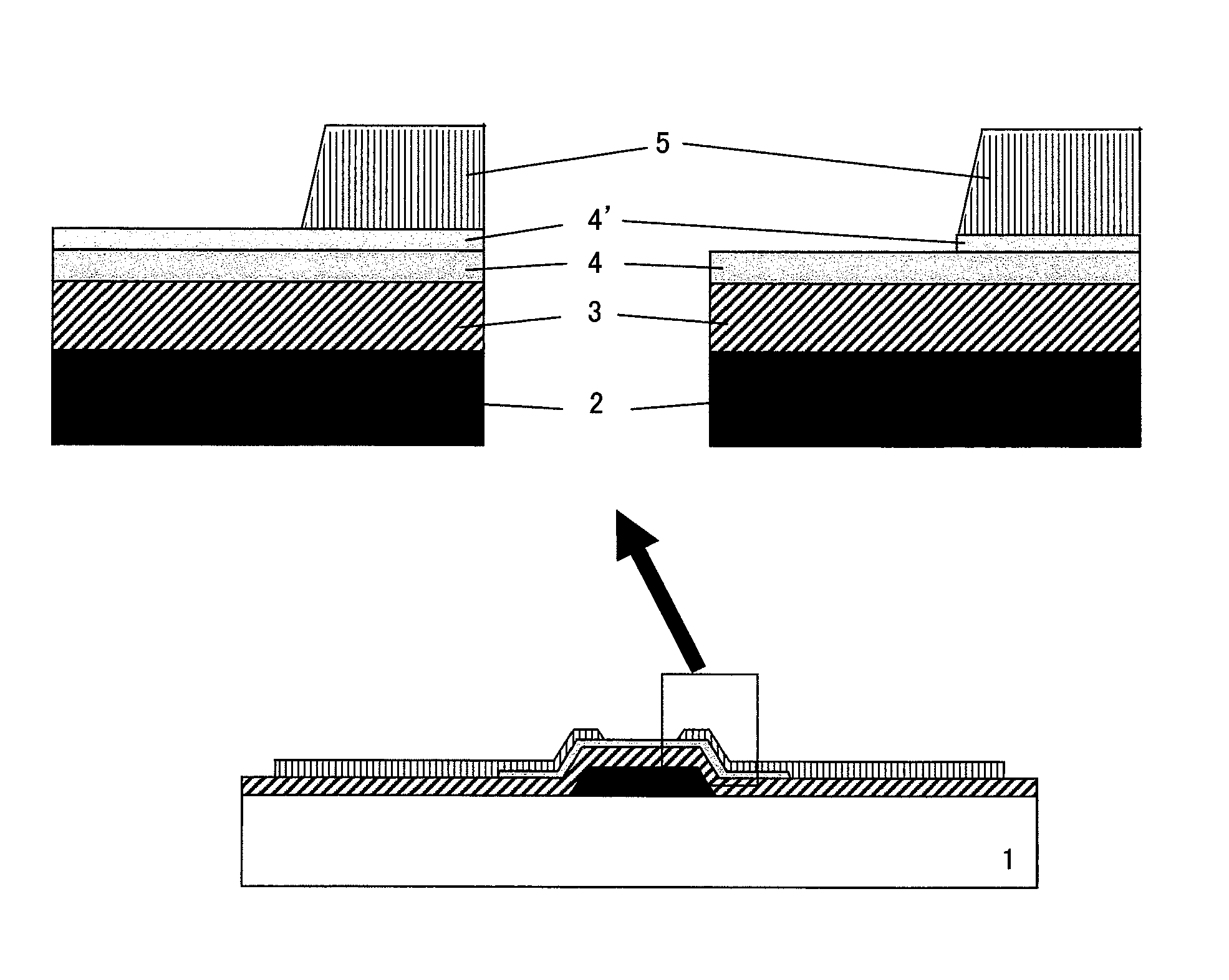
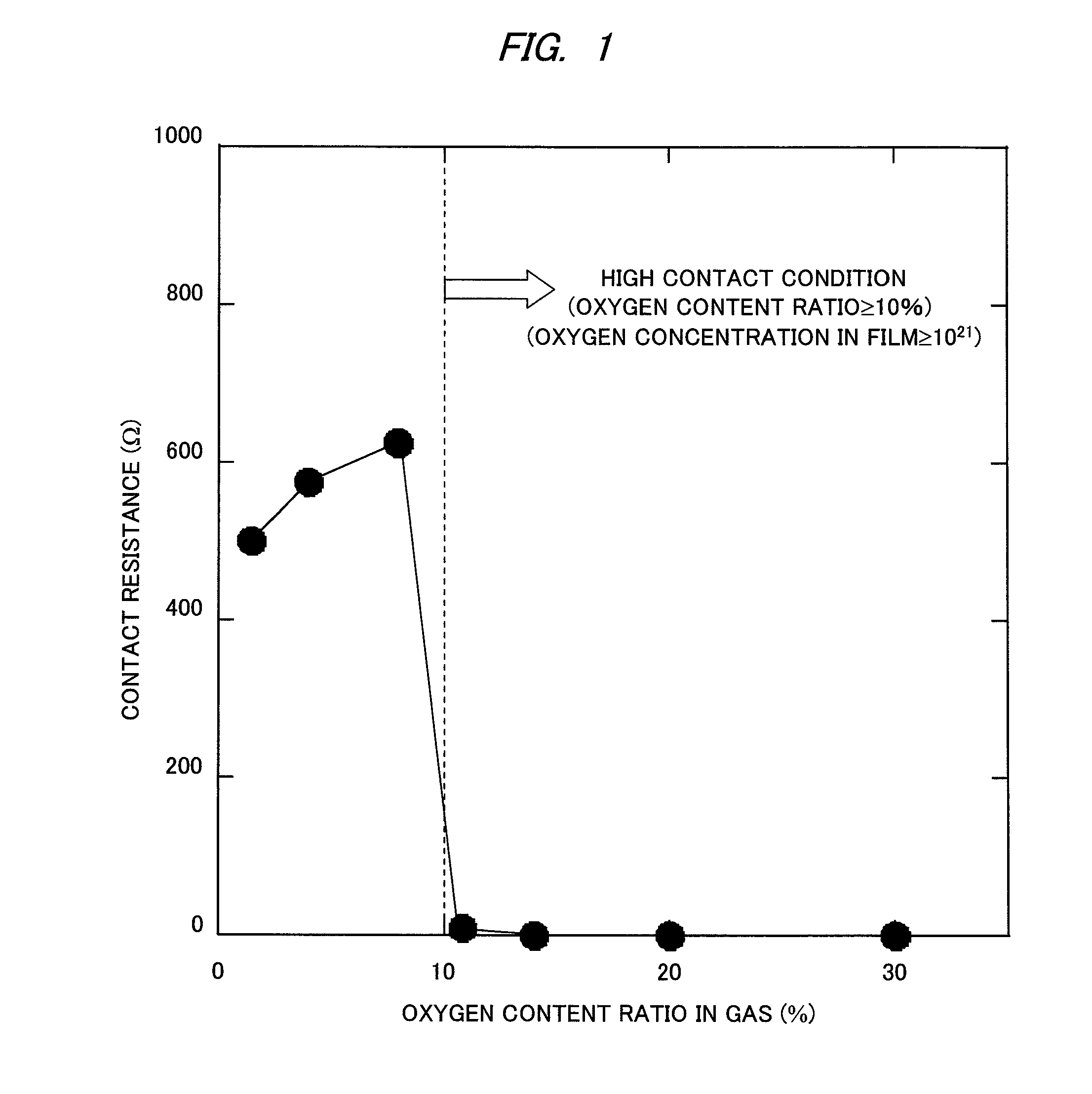
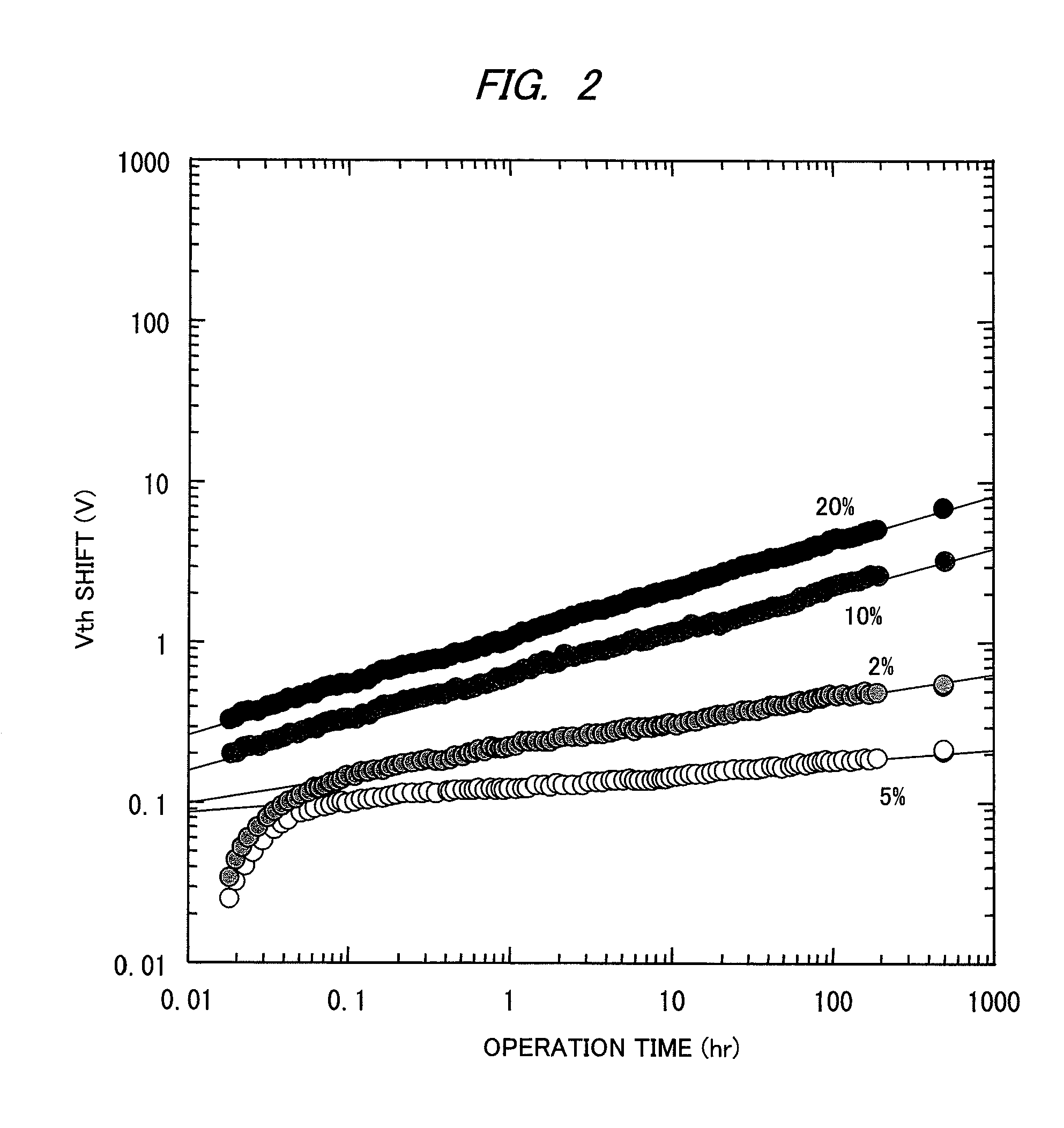
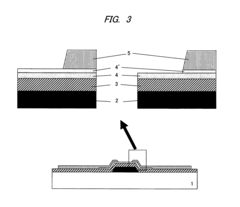
Oxide semiconductor device with oxide semiconductor layers of different oxygen concentrations and method of manufacturing the same
PatentInactiveUS8368067B2
Innovation
- A multilayered structure is implemented with an oxide semiconductor layer having a low oxygen content ratio near the gate insulating film and a high oxygen content ratio near the metal electrode, optimizing oxygen concentrations to balance contact resistance and threshold potential shift, ensuring effective ohmic contact and reliability.
Oxide Semiconductor Device and Surface Treatment Method of Oxide Semiconductor
PatentInactiveUS20140175437A1
Innovation
- A surface treatment method using oxygen group elements like sulfur or selenium is applied to passivate oxygen defects at the interface between the oxide semiconductor and gate insulator, reducing electron supplementing sites and stabilizing the device characteristics.
Environmental Impact Assessment
The environmental impact of oxide semiconductor technologies extends throughout their entire lifecycle, from raw material extraction to end-of-life disposal. Manufacturing processes for oxide semiconductors typically require fewer toxic materials compared to traditional silicon-based semiconductors, with reduced usage of arsenic and phosphorus compounds. This results in lower environmental contamination risks during production phases.
Energy consumption represents a significant environmental consideration for oxide semiconductor manufacturing. While these technologies generally operate at lower temperatures than silicon alternatives, reducing energy requirements by approximately 30%, the specific energy profile varies based on manufacturing techniques and facility efficiency. Companies implementing oxide semiconductor production should conduct comprehensive energy audits to establish baseline consumption metrics and identify optimization opportunities.
Water usage in oxide semiconductor fabrication presents both challenges and advantages. The manufacturing process typically consumes 20-40% less water than conventional semiconductor production, yet still requires substantial quantities for cleaning and cooling operations. Implementing closed-loop water recycling systems can significantly reduce consumption, with industry leaders achieving up to 80% water reuse rates in advanced facilities.
Waste management protocols for oxide semiconductor manufacturing must address both solid waste and chemical byproducts. Metal oxide residues, though generally less hazardous than traditional semiconductor waste, still require proper handling and disposal. Regulatory compliance frameworks vary by region, with the European Union's Restriction of Hazardous Substances (RoHS) and Waste Electrical and Electronic Equipment (WEEE) directives providing comprehensive guidelines for manufacturers operating in European markets.
End-of-life considerations for oxide semiconductor devices present recycling opportunities due to their relatively simpler material composition. Recovery rates for valuable metals from these components can reach 85-95% with appropriate recycling technologies, significantly higher than conventional semiconductor recovery rates. However, specialized recycling infrastructure remains limited in many regions, creating potential barriers to achieving optimal material recovery.
Carbon footprint assessments indicate that oxide semiconductor technologies can reduce lifecycle emissions by 15-25% compared to traditional alternatives when accounting for manufacturing, operation, and disposal phases. This advantage stems primarily from lower energy requirements during both production and operational stages, particularly in applications like display technologies where oxide semiconductors enable more energy-efficient designs.
Global Harmonization of Safety Standards
The global landscape of oxide semiconductor safety standards presents a fragmented regulatory environment that creates significant challenges for manufacturers, suppliers, and end-users in the electronics industry. Currently, major economic regions including the European Union, United States, China, Japan, and South Korea maintain distinct regulatory frameworks with varying requirements for material safety, testing protocols, and compliance documentation. This regulatory divergence increases compliance costs, extends time-to-market, and creates technical barriers to trade.
Efforts toward harmonization have gained momentum through international organizations such as the International Electrotechnical Commission (IEC) and the International Organization for Standardization (ISO). The IEC 62474 standard for material declaration in products of the electrotechnical industry represents a significant step toward establishing common reporting formats and substance identification protocols. Similarly, the Strategic Approach to International Chemicals Management (SAICM) provides a policy framework for promoting chemical safety globally.
Industry consortia have emerged as critical drivers of harmonization efforts. The International Electronics Manufacturing Initiative (iNEMI) and the Electronic Components Industry Association (ECIA) have established working groups specifically focused on oxide semiconductor materials standardization. These collaborative platforms facilitate knowledge sharing and consensus-building among stakeholders across the supply chain, from raw material suppliers to device manufacturers and recyclers.
Regional regulatory convergence programs demonstrate promising pathways toward global harmonization. The Mutual Recognition Agreements (MRAs) between the EU and several trading partners allow for conformity assessments conducted in one jurisdiction to be accepted in another. The Asia-Pacific Economic Cooperation (APEC) Chemical Dialogue has established frameworks for aligning chemical management systems across member economies, including those relevant to oxide semiconductor manufacturing.
Key challenges to harmonization include differing risk assessment methodologies, varying cultural and political approaches to environmental protection, and the rapid pace of technological innovation that outstrips regulatory development. The emergence of novel oxide semiconductor materials with unique properties requires adaptive regulatory frameworks that can accommodate scientific uncertainty while maintaining appropriate safety margins.
Moving forward, a multi-stakeholder approach combining technical standardization, regulatory cooperation, and industry self-regulation offers the most promising path toward global harmonization. Establishing international reference laboratories for testing methodology validation, developing shared substance databases, and implementing mutual recognition of compliance certifications would significantly reduce regulatory fragmentation while maintaining robust safety protections for human health and the environment.
Unlock deeper insights with Patsnap Eureka Quick Research — get a full tech report to explore trends and direct your research. Try now!
Generate Your Research Report Instantly with AI Agent
Supercharge your innovation with Patsnap Eureka AI Agent Platform!