

Research on Interface Engineering in Oxide Semiconductor Devices
SEP 25, 202510 MIN READ
Generate Your Research Report Instantly with AI Agent
PatSnap Eureka helps you evaluate technical feasibility & market potential.
Oxide Semiconductor Interface Engineering Background and Objectives
Oxide semiconductor interface engineering has emerged as a critical field in semiconductor technology over the past two decades. The evolution of this technology can be traced back to the early 2000s when transparent amorphous oxide semiconductors (TAOS) began gaining attention as alternatives to conventional silicon-based materials. The trajectory of development accelerated significantly after 2004 with the discovery of amorphous indium-gallium-zinc oxide (a-IGZO) by Hosono's group, which demonstrated remarkable electron mobility even in the amorphous state.
The interface between oxide semiconductors and adjacent materials plays a pivotal role in determining device performance, reliability, and functionality. These interfaces, whether with dielectrics, metals, or other semiconductors, govern charge transport, trap density, and ultimately the electrical characteristics of devices. Historical challenges in this domain have included interface instability, high defect densities, and inconsistent performance under bias stress conditions.
Current technological trends indicate a shift toward more sophisticated interface engineering approaches, including atomic layer deposition techniques, surface passivation strategies, and compositional gradient interfaces. These advancements aim to address persistent issues such as threshold voltage instability, hysteresis effects, and carrier mobility limitations that have historically constrained oxide semiconductor applications.
The primary objectives of research in oxide semiconductor interface engineering encompass several dimensions. First, to achieve atomically precise control over interface formation to minimize defect states and unwanted charge trapping. Second, to develop scalable and industry-compatible processes for interface modification that can be integrated into existing manufacturing workflows. Third, to establish comprehensive models that accurately describe charge transport mechanisms across these interfaces under various operational conditions.
Additionally, research aims to enhance device performance metrics through interface optimization, particularly focusing on mobility enhancement, subthreshold swing reduction, and operational stability improvement. The ultimate goal is to enable oxide semiconductor technologies to expand beyond their current applications in display backplanes toward more demanding applications including high-performance logic, memory, and sensing devices.
Understanding the fundamental physics and chemistry of these interfaces represents another critical objective, as theoretical insights can guide experimental approaches and accelerate innovation cycles. This includes investigating the role of oxygen vacancies, metal cation distributions, and structural disorder at interfaces, which collectively determine the electronic properties of the resulting devices.
Market Analysis for Oxide Semiconductor Device Applications
The oxide semiconductor device market has witnessed substantial growth in recent years, driven primarily by the expanding display industry and emerging applications in power electronics. The global market for oxide semiconductor devices reached approximately $5.2 billion in 2022 and is projected to grow at a CAGR of 12.3% through 2028, potentially reaching $10.4 billion by the end of the forecast period.
Display applications currently dominate the market landscape, accounting for over 70% of oxide semiconductor device consumption. This is largely attributed to the widespread adoption of IGZO (Indium Gallium Zinc Oxide) thin-film transistors in high-resolution displays, OLED panels, and flexible display technologies. Major display manufacturers including Samsung, LG Display, and BOE Technology have significantly increased their investment in oxide semiconductor technology to meet growing consumer demand for higher performance displays with lower power consumption.
The consumer electronics segment represents the largest end-user market, with applications spanning smartphones, tablets, televisions, and wearable devices. This segment is expected to maintain its dominant position through 2028, though its relative market share may decrease as other applications gain traction. The automotive sector is emerging as a particularly promising growth area, with oxide semiconductor devices increasingly incorporated into advanced driver-assistance systems, in-vehicle displays, and power management systems.
Geographically, East Asia leads the market with approximately 65% share, driven by the concentration of display manufacturing facilities and semiconductor production in countries like South Korea, Japan, China, and Taiwan. North America and Europe follow with smaller but growing market shares, primarily focused on research and development of next-generation applications.
From an application perspective, the market is witnessing diversification beyond displays. Power electronics applications are gaining significant momentum, with oxide semiconductor devices increasingly utilized in power conversion systems, renewable energy interfaces, and electric vehicle infrastructure. These applications value the wide bandgap properties and high electron mobility characteristics of oxide semiconductors.
The healthcare and industrial sectors represent emerging application areas with substantial growth potential. Medical imaging systems, biosensors, and industrial automation equipment are beginning to incorporate oxide semiconductor technology due to its stability, transparency, and performance advantages in specific operating environments.
Market analysts identify interface engineering as a critical factor influencing market adoption across all application segments. Improvements in interface quality directly correlate with device performance, reliability, and manufacturing yield – all key considerations for commercial deployment. Companies demonstrating superior interface engineering capabilities are positioned to capture premium market segments where performance requirements are most stringent.
Current Status and Technical Challenges in Interface Engineering
Interface engineering in oxide semiconductor devices has reached a critical juncture in its development trajectory. Currently, the field is experiencing significant advancements in controlling and optimizing the interfaces between oxide semiconductors and adjacent materials, which directly impacts device performance and reliability. Research institutions worldwide have demonstrated considerable progress in understanding the fundamental mechanisms governing interface formation and behavior, particularly in metal oxide semiconductor field-effect transistors (MOSFETs), thin-film transistors (TFTs), and emerging memory devices.
The state-of-the-art interface engineering techniques include atomic layer deposition (ALD), plasma-enhanced chemical vapor deposition (PECVD), and various post-deposition treatments such as thermal annealing and plasma processing. These methods have enabled precise control over interface properties at the atomic scale, resulting in improved carrier mobility, reduced interface trap density, and enhanced operational stability of oxide semiconductor devices.
Despite these advancements, several significant technical challenges persist. The most prominent issue is the presence of interface defects, including oxygen vacancies, metal interstitials, and dangling bonds, which create unwanted electronic states within the bandgap. These defects act as charge trapping centers, leading to threshold voltage instability, hysteresis effects, and degraded switching characteristics in transistor applications.
Another critical challenge lies in achieving uniform and reproducible interface properties across large-area substrates, which is essential for commercial manufacturing. The sensitivity of oxide interfaces to processing conditions creates variability issues that hamper mass production capabilities and yield rates, particularly for flexible electronics applications where substrate compatibility adds another layer of complexity.
The integration of oxide semiconductor interfaces with emerging materials such as 2D semiconductors, organic semiconductors, and ferroelectric materials presents additional challenges related to lattice matching, band alignment, and chemical compatibility. These heterogeneous integration efforts are crucial for next-generation devices but require innovative approaches to mitigate interface-related degradation mechanisms.
Environmental stability remains a persistent concern, as many oxide semiconductor interfaces exhibit sensitivity to ambient conditions, including humidity, oxygen, and light exposure. This susceptibility leads to time-dependent performance drift and reliability issues that must be addressed through effective passivation strategies and encapsulation techniques.
From a geographical perspective, research leadership in oxide semiconductor interface engineering is distributed across Asia (particularly Japan, South Korea, and China), North America, and Europe, with each region focusing on different application domains and technological approaches. This global distribution of expertise has created a competitive landscape that drives innovation but also fragments knowledge and intellectual property across multiple research ecosystems.
Current Interface Engineering Solutions and Methodologies
01 Interface engineering in oxide semiconductor devices
Interface engineering plays a crucial role in oxide semiconductor devices, particularly in managing the boundary between different materials. Proper interface design can significantly improve device performance by reducing defects, controlling charge transfer, and enhancing carrier mobility. Various techniques such as surface treatments, buffer layers, and controlled deposition methods are employed to optimize these interfaces for better electrical characteristics and device reliability.- Interface engineering in oxide semiconductor devices: Interface engineering plays a crucial role in oxide semiconductor devices, focusing on optimizing the boundary between different materials to enhance device performance. This includes controlling defects, charge trapping, and carrier transport at interfaces. Proper interface engineering can significantly improve electron mobility, reduce threshold voltage shifts, and enhance overall device stability. Various techniques such as surface treatments, buffer layers, and passivation methods are employed to modify interface properties.
- Metal oxide semiconductor field-effect transistor (MOSFET) gate interfaces: The gate interface in metal oxide semiconductor field-effect transistors is critical for device operation. This interface typically consists of a gate dielectric layer between the semiconductor channel and the gate electrode. The quality of this interface affects key parameters such as threshold voltage, subthreshold swing, and carrier mobility. Advanced processing techniques are used to minimize interface states, reduce fixed charges, and prevent impurity diffusion across the interface, resulting in improved electrical characteristics and reliability.
- Transparent oxide semiconductor interfaces for display applications: Transparent oxide semiconductors, such as indium gallium zinc oxide (IGZO), are widely used in display technologies. The interfaces between these oxide semiconductors and other materials (electrodes, insulators) significantly impact display performance. Optimizing these interfaces helps achieve high transparency, good electrical conductivity, and stable switching characteristics. Special attention is given to reducing contact resistance, improving carrier injection, and enhancing long-term stability under various operating conditions.
- Characterization and analysis of oxide semiconductor interfaces: Various analytical techniques are employed to characterize oxide semiconductor interfaces at the atomic and electronic levels. These include scanning probe microscopy, X-ray photoelectron spectroscopy, transmission electron microscopy, and electrical measurements. Such characterization helps understand interface phenomena such as band alignment, defect formation, and charge distribution. This knowledge is essential for developing models that predict device behavior and guide the design of improved interfaces with enhanced electrical properties.
- Passivation and stability of oxide semiconductor interfaces: Passivation techniques are crucial for stabilizing oxide semiconductor interfaces against environmental factors and operational stress. Various materials and processes are used to neutralize dangling bonds, remove contaminants, and create protective barriers. Effective passivation reduces interface trap density, prevents moisture ingress, and mitigates bias stress instability. This results in devices with improved reliability, longer operational lifetimes, and consistent performance under various environmental conditions.
02 Gate dielectric interfaces for oxide semiconductor transistors
The interface between gate dielectrics and oxide semiconductors is critical for transistor performance. This interface affects channel formation, carrier concentration, and threshold voltage stability. High-quality gate dielectric interfaces with minimal trap states and defects are essential for achieving high mobility, low leakage current, and stable operation in oxide semiconductor transistors. Various dielectric materials and deposition techniques are employed to optimize this interface region.Expand Specific Solutions03 Contact interfaces and electrode structures
The contact interfaces between oxide semiconductors and metal electrodes significantly impact device performance. These interfaces determine contact resistance, carrier injection efficiency, and overall device reliability. Various approaches including metal selection, interface modification layers, and annealing treatments are used to create ohmic contacts with low resistance. Proper design of source/drain electrodes and their interfaces with oxide semiconductors is essential for achieving high-performance devices.Expand Specific Solutions04 Multilayer oxide semiconductor interfaces
Multilayer structures involving different oxide semiconductor compositions create internal interfaces that can be engineered to enhance device performance. These heterojunction interfaces allow for band engineering, carrier confinement, and improved stability. By carefully designing the composition and thickness of each layer, properties such as carrier mobility, off-state current, and bias stress stability can be optimized. These multilayer approaches enable more sophisticated device architectures with enhanced functionality.Expand Specific Solutions05 Passivation and encapsulation interfaces
The external interfaces of oxide semiconductor devices with passivation and encapsulation layers are crucial for long-term stability and reliability. These interfaces protect the active device regions from environmental factors such as moisture, oxygen, and contaminants that can degrade performance. Various passivation materials and techniques are employed to minimize interface states, prevent ion migration, and maintain stable electrical characteristics throughout the device lifetime.Expand Specific Solutions
Key Industry Players in Oxide Semiconductor Device Development
The interface engineering landscape in oxide semiconductor devices is currently in a growth phase, with the market expanding due to increasing demand for high-performance electronics. The global competition is intensifying as major players like Taiwan Semiconductor Manufacturing Co., GLOBALFOUNDRIES, and Micron Technology invest heavily in research. Japanese companies including Semiconductor Energy Laboratory, Japan Display, and KIOXIA are particularly strong in oxide semiconductor innovation. Academic institutions such as University of Tokyo and Vanderbilt University collaborate with industry leaders to advance fundamental research. The technology is approaching maturity for display applications but remains in development for advanced computing and power electronics, with companies like Applied Materials and NXP USA focusing on manufacturing process improvements to enhance device performance and reliability.
Semiconductor Energy Laboratory Co., Ltd.
Technical Solution: Semiconductor Energy Laboratory (SEL) has pioneered advanced interface engineering techniques for oxide semiconductor devices, particularly focusing on IGZO (Indium Gallium Zinc Oxide) technology. Their approach involves precise control of oxygen vacancies at semiconductor-insulator interfaces through innovative passivation methods and thermal treatments. SEL has developed proprietary hydrogen-based passivation techniques that effectively neutralize dangling bonds at interfaces, significantly reducing trap states and enhancing carrier mobility[1]. Their research extends to multi-layer oxide structures with carefully engineered compositional gradients at interfaces to minimize lattice mismatch and reduce interface defect density. SEL has also implemented advanced atomic layer deposition (ALD) processes for creating high-quality gate insulators with controlled interface formation, resulting in devices with exceptional stability under bias stress conditions and reduced hysteresis effects[2].
Strengths: Industry-leading expertise in IGZO technology with superior interface control techniques resulting in higher mobility and stability. Extensive patent portfolio covering interface engineering methods. Weaknesses: Their advanced processes may require specialized equipment with higher manufacturing costs compared to conventional silicon-based technologies.
Applied Materials, Inc.
Technical Solution: Applied Materials has developed comprehensive interface engineering solutions for oxide semiconductor manufacturing through their advanced deposition and treatment systems. Their approach centers on integrated process solutions that address the entire interface formation sequence. Applied Materials' Endura® platform incorporates specialized pre-deposition surface preparation chambers that use controlled plasma treatments to create optimal surface conditions before oxide semiconductor deposition[5]. They have pioneered advanced reactive sputtering techniques with real-time plasma monitoring to precisely control oxygen incorporation at interfaces. Their research extends to post-deposition interface modification using proprietary remote plasma nitridation and oxidation processes that selectively modify interface chemistry without damaging the underlying layers. Applied Materials has also developed specialized annealing systems with precise temperature and atmosphere control that enable interface reconstruction and defect passivation through carefully controlled thermal budgets[6]. Their holistic approach addresses both the semiconductor-dielectric and semiconductor-contact interfaces.
Strengths: Comprehensive equipment portfolio covering the entire interface engineering process chain. Strong position as equipment supplier to major semiconductor manufacturers enables broad industry impact. Weaknesses: As an equipment manufacturer, they depend on adoption of their specific tools by device manufacturers, which may limit implementation of some advanced techniques.
Critical Patents and Technical Literature in Interface Engineering
Metal oxide semiconductor device and method of manufacturing semiconductor device
PatentInactiveJP2016105502A
Innovation
- A method involving interfacial interaction control through material selection and surface treatment at the lower and upper interfaces of the metal oxide active layer, using inert and active materials to adjust oxygen content and carrier density, and deposition methods to modify oxygen levels in the metal oxide.
Semiconductor device having reduced oxidation interface
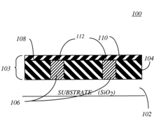
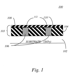
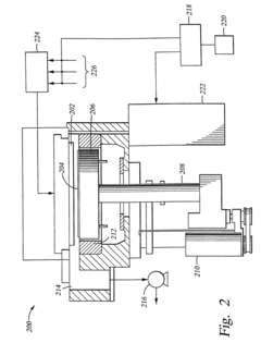
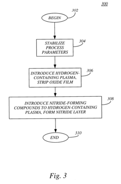
PatentInactiveUS6700202B2
Innovation
- A method involving a hydrogen-containing plasma treatment with ammonia, followed by the introduction of silane and nitrogen to form a continuous plasma-enhanced CVD process, which reduces oxidation and promotes adhesion of subsequent insulating layers on semiconductor devices, specifically using a power range of 50-500 W and flow rates of 50-300 sccm for ammonia and 220 sccm for silane, performed in a controlled environment to minimize cross-contamination.
Materials Science Advancements for Enhanced Interface Properties
Recent advancements in materials science have significantly contributed to enhancing interface properties in oxide semiconductor devices. The development of novel deposition techniques has enabled precise control over interface formation at the atomic level. Atomic Layer Deposition (ALD) has emerged as a particularly valuable method, allowing for angstrom-level precision in creating uniform and conformal thin films with minimal defects at critical interfaces.
High-k dielectric materials have revolutionized interface engineering by providing superior insulating properties while maintaining good compatibility with oxide semiconductors. Materials such as HfO2, Al2O3, and ZrO2 have demonstrated excellent capacitance characteristics while minimizing leakage current, addressing one of the fundamental challenges in oxide semiconductor device performance.
Surface passivation techniques have evolved substantially, with hydrogen, nitrogen, and sulfur-based treatments showing remarkable effectiveness in reducing interface trap densities. These treatments neutralize dangling bonds at interfaces, significantly decreasing electron scattering and improving carrier mobility across device junctions. The introduction of self-assembled monolayers (SAMs) as interface modifiers has further enhanced this approach by providing customizable surface properties.
Two-dimensional materials integration represents another breakthrough in interface engineering. Materials like graphene, MoS2, and h-BN have been successfully incorporated at oxide semiconductor interfaces, creating atomically sharp junctions with minimal lattice mismatch. These 2D materials serve as effective buffer layers, reducing strain and preventing unwanted diffusion between adjacent materials.
Computational materials science has accelerated interface optimization through density functional theory (DFT) and molecular dynamics simulations. These computational approaches enable researchers to predict interface behaviors, identify optimal material combinations, and understand atomic-level interactions before experimental implementation, significantly reducing development cycles.
Defect engineering strategies have been refined to manipulate interface states deliberately. Controlled introduction of specific defects or dopants at interfaces can create beneficial band alignments, enhance carrier transport, or establish desirable electrical characteristics. This approach transforms traditionally problematic defects into functional elements of device design.
Advanced characterization techniques, including high-resolution transmission electron microscopy (HRTEM), X-ray photoelectron spectroscopy (XPS), and scanning tunneling microscopy (STM), have provided unprecedented insights into interface structures and properties, enabling more targeted materials development and process optimization for next-generation oxide semiconductor devices.
Sustainability and Environmental Impact of Oxide Semiconductor Fabrication
The environmental impact of oxide semiconductor fabrication processes has become increasingly important as these technologies gain wider adoption in consumer electronics, displays, and power devices. Traditional semiconductor manufacturing processes are known for their significant resource consumption and environmental footprint, making sustainability a critical consideration for the oxide semiconductor industry.
Manufacturing processes for oxide semiconductors typically involve vacuum deposition techniques such as sputtering, pulsed laser deposition, and atomic layer deposition. These methods generally require less energy and fewer toxic chemicals compared to conventional silicon-based semiconductor fabrication. However, they still present environmental challenges that must be addressed through careful engineering and process optimization.
Water usage represents a significant environmental concern in oxide semiconductor production. The industry has been implementing water recycling systems and developing dry etching processes to reduce consumption. Recent advancements have demonstrated up to 30% reduction in water usage through closed-loop systems that purify and recirculate process water, significantly reducing the environmental burden on local water resources.
Energy efficiency improvements have been achieved through optimized deposition processes that operate at lower temperatures. While traditional oxide semiconductor fabrication often required high-temperature annealing (400-600°C), newer interface engineering approaches have enabled processing temperatures below 300°C, reducing energy consumption and allowing for compatibility with flexible substrates.
Chemical waste management presents another sustainability challenge. The industry has been transitioning away from toxic precursors and etchants containing heavy metals and fluorinated compounds. Alternative, environmentally benign materials are being developed, including water-based solutions and biodegradable chemicals that maintain performance while reducing environmental impact.
Life cycle assessment studies indicate that oxide semiconductor devices generally have a lower carbon footprint than conventional silicon technologies when considering the entire product lifecycle. This advantage stems from lower processing temperatures, fewer fabrication steps, and reduced material requirements. However, end-of-life recycling remains challenging due to the complex material interfaces in these devices.
Future sustainability improvements will likely focus on circular economy approaches, including design for disassembly and material recovery. Research into biologically derived precursors and green chemistry principles is showing promise for further reducing the environmental impact of interface engineering in oxide semiconductor fabrication, potentially enabling truly sustainable electronics manufacturing processes.
Unlock deeper insights with PatSnap Eureka Quick Research — get a full tech report to explore trends and direct your research. Try now!
Generate Your Research Report Instantly with AI Agent
Supercharge your innovation with PatSnap Eureka AI Agent Platform!