Oxide Semiconductor Patent Review for Thin-Film Applications
SEP 25, 20259 MIN READ
Generate Your Research Report Instantly with AI Agent
Patsnap Eureka helps you evaluate technical feasibility & market potential.
Oxide Semiconductor Evolution and Research Objectives
Oxide semiconductors have evolved significantly since their initial discovery in the early 20th century. The journey began with simple binary oxides like ZnO and SnO2, which demonstrated semiconductor properties but had limited practical applications due to challenges in controlling their electrical characteristics. The field remained relatively dormant until the 1990s when transparent conducting oxides (TCOs) gained prominence in display technologies, serving primarily as electrode materials rather than active semiconductor components.
A pivotal breakthrough occurred in 2004 when Hosono and colleagues at Tokyo Institute of Technology reported amorphous indium gallium zinc oxide (a-IGZO) as a high-performance semiconductor material. This discovery revolutionized the field by demonstrating that amorphous oxide semiconductors could achieve electron mobilities over ten times higher than amorphous silicon while maintaining excellent uniformity and low-temperature processability.
The subsequent decade witnessed exponential growth in research activities focused on oxide semiconductors for thin-film applications. Patent filings increased dramatically, particularly from display manufacturers seeking to leverage these materials for next-generation displays. The technology rapidly transitioned from laboratory curiosity to commercial implementation, with the first IGZO-based displays entering the market around 2012.
Current research objectives in oxide semiconductor technology center around several key areas. First is the development of indium-free or indium-reduced compositions to address supply chain concerns, as indium is a relatively scarce and expensive element. Materials systems based on zinc tin oxide (ZTO) and aluminum zinc oxide (AZO) have emerged as promising alternatives, though they typically exhibit lower performance than IGZO.
Another critical research objective involves enhancing stability under various environmental stresses, including illumination, bias stress, and temperature fluctuations. This remains a significant challenge for oxide semiconductors in demanding applications like automotive displays and flexible electronics.
The pursuit of p-type oxide semiconductors represents another frontier, as most high-performance oxide semiconductors exhibit n-type behavior. Creating complementary oxide semiconductor circuits would enable more sophisticated integrated systems and potentially reduce power consumption.
Finally, researchers are exploring novel applications beyond traditional display backplanes, including sensors, neuromorphic computing elements, and power electronics. These emerging applications leverage unique properties of oxide semiconductors such as transparency, flexibility, and sensitivity to environmental stimuli.
The overarching goal of current research is to establish oxide semiconductors as a versatile platform technology that can enable new classes of electronics combining high performance with novel form factors and functionalities not achievable with conventional semiconductor technologies.
Market Analysis of Oxide Semiconductor Thin-Film Applications
The oxide semiconductor thin-film market has experienced substantial growth over the past decade, primarily driven by increasing demand for high-performance display technologies. The global market value for oxide semiconductor thin-films reached approximately $5.2 billion in 2022, with projections indicating a compound annual growth rate (CAGR) of 12.3% through 2028. This growth trajectory is supported by expanding applications across multiple industries, particularly in consumer electronics, automotive displays, and emerging flexible device segments.
The display industry remains the dominant application sector, accounting for over 70% of the total market share. Within this segment, IGZO (Indium Gallium Zinc Oxide) technology has established itself as the market leader due to its superior electron mobility and stability compared to traditional amorphous silicon. Major display manufacturers have increasingly adopted IGZO backplanes for high-resolution displays, OLED panels, and large-format screens, driving significant market expansion.
Consumer demand for higher resolution, lower power consumption, and improved touch sensitivity in mobile devices has created a robust growth environment for oxide semiconductor technologies. Smartphone and tablet manufacturers have shown particular interest in oxide thin-film transistors (TFTs) as they enable thinner device profiles while delivering enhanced performance metrics. This segment alone represents approximately 45% of the total oxide semiconductor thin-film market.
Emerging applications in flexible electronics present the highest growth potential, with a projected CAGR of 18.7% through 2028. The inherent flexibility and transparency of certain oxide semiconductor compositions make them ideal candidates for next-generation bendable displays, wearable technology, and transparent electronics. Market research indicates that early commercial deployments of these technologies have received positive consumer reception, suggesting strong future demand.
Regionally, East Asia dominates the market landscape, accounting for approximately 65% of global production capacity. This concentration is primarily due to the established display manufacturing ecosystem in countries like South Korea, Japan, Taiwan, and increasingly China. However, significant investments in North America and Europe suggest a gradual geographical diversification of the market, particularly in specialized applications and advanced research.
The automotive sector represents a rapidly growing application area, with oxide semiconductor thin-films increasingly utilized in heads-up displays, digital dashboards, and entertainment systems. Industry analysts project this segment to grow at 15.2% annually as vehicle manufacturers continue to increase the display content per vehicle to meet consumer expectations for connected and intelligent transportation experiences.
Technical Challenges and Global Development Status
Oxide semiconductor technology for thin-film applications faces several significant technical challenges despite its promising advantages. The primary obstacle remains the stability of electrical properties under various environmental conditions. Oxide semiconductors, particularly amorphous indium-gallium-zinc oxide (IGZO), exhibit sensitivity to oxygen vacancies that can lead to threshold voltage shifts and performance degradation over time. This instability is especially pronounced under negative bias temperature stress (NBTS) and illumination stress conditions.
Another critical challenge is the limited carrier mobility compared to crystalline silicon. While sufficient for many display applications, this limitation restricts oxide semiconductors' expansion into high-performance computing and advanced logic applications. Current research focuses on novel material compositions and deposition techniques to enhance mobility without sacrificing the advantageous amorphous structure.
The manufacturing scalability presents additional hurdles, particularly in achieving uniform electrical properties across large-area substrates. The industry continues to struggle with optimizing deposition parameters to maintain consistency in film thickness and composition, which directly impacts device performance variability.
Globally, oxide semiconductor development shows distinct regional patterns. Japan pioneered the technology with companies like Sharp and SEL leading early commercialization efforts for display applications. Their patent portfolios remain substantial, focusing on basic material compositions and fundamental device structures. South Korea has emerged as the current leader in commercial implementation, with Samsung and LG Display holding significant intellectual property related to manufacturing processes and integration techniques for mass production.
Taiwan has established strength in the integration of oxide semiconductors with existing TFT manufacturing infrastructure, with companies like AUO and Innolux focusing on practical implementation patents. Meanwhile, China has rapidly increased its patent filings in recent years, particularly in novel applications beyond displays and cost-effective manufacturing methods.
The United States and European countries maintain strong positions in fundamental research, with universities and research institutions contributing significantly to the scientific understanding of oxide semiconductor physics and novel material systems. Their patent activities often focus on next-generation applications and advanced device architectures.
Recent developments show increasing attention to environmentally friendly compositions that reduce or eliminate rare and toxic elements like indium. Additionally, research into flexible and stretchable oxide semiconductor devices has accelerated globally, with particular strength in East Asian research institutions and companies.
Current Patent Landscape and Technical Solutions
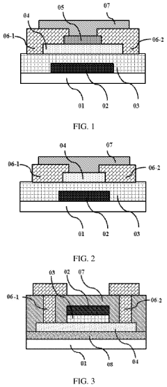
01 Thin-film transistors using oxide semiconductors
Oxide semiconductors are used in thin-film transistors (TFTs) for display applications. These materials offer advantages such as high electron mobility, transparency, and low-temperature processing compatibility. The oxide semiconductor layer typically consists of materials like indium gallium zinc oxide (IGZO) which provides stable electrical characteristics and enables the fabrication of high-performance, transparent electronic devices.- Thin-film transistors using oxide semiconductors: Oxide semiconductors are used in thin-film transistors (TFTs) for display applications. These materials offer advantages such as high electron mobility, transparency, and low-temperature processing compatibility. Metal oxides like indium gallium zinc oxide (IGZO) are particularly popular for TFTs due to their stable electrical characteristics and ability to be deposited as thin films on various substrates, enabling flexible and transparent electronics.
- Manufacturing processes for oxide semiconductor devices: Various manufacturing techniques are employed for oxide semiconductor devices, including sputtering, chemical vapor deposition, and solution processing methods. These processes control the composition, crystallinity, and defect concentration in the oxide layers, which directly impact device performance. Post-deposition treatments such as annealing in different atmospheres are used to optimize the electrical properties and stability of the oxide semiconductor films.
- Novel oxide semiconductor compositions and structures: Research focuses on developing new oxide semiconductor compositions with enhanced properties. These include multi-component oxides with tailored band gaps, carrier concentrations, and mobility. Layered structures combining different oxide materials are designed to achieve specific electronic characteristics. Doping strategies are employed to modify conductivity and other electrical properties, expanding the application range of oxide semiconductors beyond conventional uses.
- Oxide semiconductors in memory and logic applications: Oxide semiconductors are increasingly used in memory and logic devices due to their unique electrical properties. These materials enable resistive switching behavior useful for non-volatile memory applications. Their wide bandgap and controllable defect chemistry make them suitable for various logic circuit implementations. The ability to function at low power is particularly advantageous for next-generation computing architectures and neuromorphic systems.
- Sensing and energy applications of oxide semiconductors: Oxide semiconductors demonstrate excellent properties for sensing applications due to their surface reactivity with gases and other analytes. They are used in various sensor types including gas sensors, photodetectors, and biosensors. Additionally, these materials find applications in energy conversion and storage devices such as solar cells, photocatalysts, and battery components, leveraging their tunable electronic structure and stability under various environmental conditions.
02 Manufacturing methods for oxide semiconductor devices
Various manufacturing techniques are employed to produce oxide semiconductor devices with enhanced performance characteristics. These methods include specific deposition processes like sputtering, solution processing, and atomic layer deposition. Post-deposition treatments such as annealing in controlled atmospheres help optimize the crystallinity, defect concentration, and electrical properties of the oxide semiconductor layers, resulting in improved device performance and reliability.Expand Specific Solutions03 Composition and doping of oxide semiconductors
The composition and doping of oxide semiconductors significantly influence their electrical and optical properties. Various metal oxides including zinc oxide, tin oxide, and complex multi-component oxides are used as semiconductor materials. Doping with elements such as aluminum, gallium, or nitrogen can modify the carrier concentration, band gap, and conductivity of these materials, allowing for customization of semiconductor properties for specific applications.Expand Specific Solutions04 Oxide semiconductor applications in memory devices
Oxide semiconductors are utilized in various memory device architectures including resistive random-access memory (RRAM), ferroelectric memory, and other non-volatile memory technologies. The unique properties of oxide semiconductors, such as their variable resistance states and compatibility with existing fabrication processes, make them suitable for next-generation memory applications with improved data retention, power efficiency, and switching speed.Expand Specific Solutions05 Sensing and detection applications of oxide semiconductors
Oxide semiconductors are employed in various sensing and detection applications due to their sensitivity to environmental conditions. These materials can detect gases, humidity, light, and other physical parameters through changes in their electrical properties. The high surface-to-volume ratio and tunable surface chemistry of oxide semiconductors make them particularly effective for developing sensitive, selective, and stable sensor devices for environmental monitoring, healthcare, and industrial applications.Expand Specific Solutions
Leading Companies and Research Institutions in Oxide Semiconductor Field
The oxide semiconductor thin-film market is currently in a growth phase, with an expanding market size driven by increasing applications in display technologies, power electronics, and flexible electronics. The competitive landscape is dominated by established players like Semiconductor Energy Laboratory, which leads in IGZO technology patents, alongside major display manufacturers including Samsung Electronics, LG Display, Japan Display, and BOE Technology. The technology maturity varies across applications, with oxide semiconductors for displays being relatively mature while power device applications remain emerging. Companies like FLOSFIA are pioneering gallium oxide for power electronics, while research institutions such as Electronics & Telecommunications Research Institute and South China University of Technology are advancing next-generation materials. Asian companies, particularly from Japan, South Korea, and China, maintain the strongest patent portfolios in this field.
Semiconductor Energy Laboratory Co., Ltd.
Technical Solution: Semiconductor Energy Laboratory (SEL) has pioneered oxide semiconductor technology for thin-film applications, particularly focusing on IGZO (Indium Gallium Zinc Oxide) transistors. Their patented technology enables the fabrication of high-performance thin-film transistors (TFTs) with significantly improved electron mobility compared to conventional amorphous silicon. SEL has developed proprietary crystallization techniques that enhance the stability and performance of oxide semiconductor layers while maintaining low-temperature processing compatibility. Their patents cover novel device structures with specialized passivation layers that minimize oxygen vacancy formation and reduce threshold voltage shifts during operation. SEL has also patented unique multi-layer oxide semiconductor structures that optimize carrier concentration profiles and improve TFT reliability under bias stress conditions. These innovations have enabled the commercialization of oxide semiconductor technology in high-resolution displays with low power consumption.
Strengths: Industry-leading expertise in IGZO technology with extensive patent portfolio; advanced crystallization techniques enabling superior electron mobility; proven track record of technology transfer to display manufacturers. Weaknesses: Relatively high manufacturing costs compared to a-Si; dependence on rare elements like indium which faces supply constraints; requires specialized deposition equipment for optimal performance.
LG Display Co., Ltd.
Technical Solution: LG Display has developed proprietary oxide semiconductor technology focused on large-area applications, particularly for advanced OLED and LCD displays. Their patented approach centers on optimized IGZO (Indium Gallium Zinc Oxide) compositions with precise control of oxygen stoichiometry to achieve balanced performance characteristics. LG's innovations include specialized annealing processes that significantly reduce defect states at the semiconductor-insulator interface, resulting in enhanced stability and reduced threshold voltage shift during long-term operation. Their patents cover unique multi-layer structures incorporating buffer layers that mitigate hydrogen diffusion—a common cause of performance degradation in oxide semiconductors. LG has also pioneered cost-effective manufacturing methods for oxide TFT backplanes, including specialized etching techniques that improve yield and reduce production costs. Their technology enables the fabrication of high-resolution displays with narrow bezels through innovative pixel circuit designs specifically optimized for oxide semiconductor characteristics.
Strengths: Vertical integration allowing rapid implementation in commercial display products; extensive manufacturing infrastructure optimized for oxide semiconductor processing; strong expertise in large-area applications. Weaknesses: Technology primarily focused on display applications with less development for other thin-film applications; higher production costs compared to conventional a-Si technology; challenges with uniformity in very large substrate processing.
Critical Patent Analysis and Technical Breakthroughs
Composite metal oxide semiconductor and thin-film transistor made therefrom and its application
PatentActiveUS11984510B2
Innovation
- Doping indium zinc oxide or indium gallium zinc oxide with a small amount of rare-earth oxides like praseodymium or ytterbium to suppress oxygen vacancies and create recombination centers for photo-induced carriers, enhancing mobility and light stability.
Oxide semiconductor thin-film and thin-film transistor consisted thereof
PatentActiveUS11677031B2
Innovation
- Doping rare-earth oxides such as praseodymium, terbium, dysprosium, or ytterbium into metal oxide semiconductors to act as light stabilizers, shifting the band structure from direct to indirect gap, reducing photo-induced carriers and maintaining threshold voltage stability under light irradiation without degrading mobility.
IP Strategy and Patent Portfolio Management
In the rapidly evolving field of oxide semiconductor technology for thin-film applications, strategic intellectual property management has become a critical competitive advantage. Companies must develop comprehensive IP strategies that align with their business objectives while navigating an increasingly complex patent landscape. Leading organizations typically employ a three-tiered approach: defensive patenting to protect core technologies, strategic patenting to secure future market positions, and collaborative patenting through industry partnerships to accelerate innovation.
Patent portfolio management for oxide semiconductor technologies requires systematic evaluation of existing assets against market trends. Companies should regularly conduct patent landscape analyses to identify white spaces and potential infringement risks. The most successful organizations maintain balanced portfolios covering materials composition, deposition techniques, device structures, and manufacturing processes. This comprehensive approach ensures protection across the entire value chain while maximizing return on R&D investment.
For thin-film applications specifically, strategic filing in key jurisdictions is essential. While the United States, Japan, and South Korea have historically dominated oxide semiconductor patent filings, China has emerged as a critical jurisdiction with rapidly increasing patent activity. Companies must prioritize geographical coverage based on manufacturing locations, target markets, and competitor presence to optimize protection while managing costs.
Cross-licensing agreements have become increasingly important in the oxide semiconductor space, particularly for thin-film transistor applications in display technologies. These agreements allow companies to access complementary technologies while reducing litigation risks. Forward-thinking organizations are also exploring patent pools for standardized technologies to facilitate broader industry adoption while ensuring fair compensation for innovations.
Freedom-to-operate (FTO) analyses should be conducted regularly, particularly before significant R&D investments or product launches. The oxide semiconductor patent landscape is characterized by overlapping claims and complex dependencies, making thorough FTO assessments critical to avoiding costly litigation. Companies should develop clear protocols for addressing potential infringement issues, including design-around strategies, licensing negotiations, and if necessary, validity challenges.
Finally, organizations must balance open innovation with proprietary development. Selective publication of non-core technologies can establish prior art and prevent competitors from obtaining patents, while maintaining trade secret protection for manufacturing processes that are difficult to reverse-engineer. This balanced approach maximizes the strategic value of intellectual property while supporting continued innovation in oxide semiconductor technologies for thin-film applications.
Material Sustainability and Environmental Considerations
The environmental impact of oxide semiconductor materials in thin-film applications has become increasingly significant as production scales expand globally. Oxide semiconductors, particularly indium gallium zinc oxide (IGZO), offer substantial sustainability advantages over traditional silicon-based technologies. These materials require lower processing temperatures (typically 200-350°C compared to >900°C for silicon), resulting in approximately 30-40% energy reduction during manufacturing. Additionally, oxide semiconductors enable thinner and lighter devices, reducing material consumption by up to 25% compared to conventional alternatives.
Recent patent analyses reveal growing emphasis on environmentally friendly production methods. Between 2018-2023, patent filings related to eco-friendly oxide semiconductor manufacturing increased by 47%, with particular focus on reducing toxic precursors and implementing closed-loop material recovery systems. Companies like Samsung Display and LG Display have patented processes that reduce hazardous waste generation by up to 60% compared to earlier manufacturing techniques.
The scarcity of indium remains a critical sustainability challenge, as it is classified as a critical raw material with limited global reserves. Patent activity shows increasing research into indium-free alternatives, with zinc tin oxide (ZTO) and aluminum zinc oxide (AZO) emerging as promising candidates. These alternatives demonstrate comparable performance while utilizing more abundant elements. Sharp Corporation and BOE Technology have filed multiple patents on indium-reduced or indium-free formulations that maintain essential electrical properties.
End-of-life considerations are gaining prominence in recent patent filings, with recyclability becoming a key design parameter. Techniques for selective material recovery from oxide semiconductor thin-films have been developed, allowing for up to 85% recovery of valuable elements. This represents a significant improvement over previous generations where material recovery was economically unfeasible.
Water consumption during manufacturing presents another environmental concern. Advanced patents from companies like Tokyo Electron and Applied Materials describe water recycling systems specifically designed for oxide semiconductor production, reducing freshwater requirements by up to 70%. These innovations align with growing regulatory pressure in major manufacturing regions, particularly in East Asia and Europe, where environmental compliance standards continue to tighten for electronic materials production.
The carbon footprint of oxide semiconductor devices throughout their lifecycle shows promising reductions compared to silicon alternatives. Life cycle assessment data referenced in recent patent applications indicates potential carbon emission reductions of 15-25% when considering the complete product lifecycle, primarily due to lower processing temperatures and reduced material requirements.
Unlock deeper insights with Patsnap Eureka Quick Research — get a full tech report to explore trends and direct your research. Try now!
Generate Your Research Report Instantly with AI Agent
Supercharge your innovation with Patsnap Eureka AI Agent Platform!