

Oxide Semiconductor Material Optimization for Transparent Electronics
SEP 25, 20259 MIN READ
Generate Your Research Report Instantly with AI Agent
PatSnap Eureka helps you evaluate technical feasibility & market potential.
Oxide Semiconductor Evolution and Objectives
Oxide semiconductors have evolved significantly since their initial discovery in the early 20th century. The journey began with the identification of basic oxide materials like zinc oxide (ZnO) and tin oxide (SnO2), which demonstrated semiconductor properties but had limited practical applications due to poor stability and performance characteristics. The field remained relatively dormant until the 1960s when transparent conducting oxides (TCOs) began gaining attention for applications in optoelectronic devices.
A pivotal moment occurred in 2004 when Hosono and colleagues at the Tokyo Institute of Technology reported on amorphous indium gallium zinc oxide (a-IGZO) thin-film transistors with remarkably high electron mobility compared to conventional amorphous silicon. This breakthrough catalyzed renewed interest in oxide semiconductors for transparent electronics, marking the beginning of the modern era of oxide semiconductor development.
The evolution accelerated in the 2010s with the emergence of solution-processed oxide semiconductors, enabling low-cost manufacturing techniques compatible with large-area electronics. Simultaneously, researchers began exploring alternative material compositions to address the scarcity and cost concerns associated with indium, leading to the development of indium-free oxide semiconductors such as zinc tin oxide (ZTO) and aluminum zinc oxide (AZO).
Recent years have witnessed significant advancements in understanding the fundamental physics and defect chemistry of oxide semiconductors. Researchers have identified the critical role of oxygen vacancies, metal interstitials, and hydrogen incorporation in determining carrier concentration and mobility. This deeper understanding has enabled more precise control over material properties through composition engineering and processing optimization.
The primary objectives in oxide semiconductor material optimization for transparent electronics center around several key performance metrics. First is achieving high electron mobility (>10 cm²/Vs) while maintaining optical transparency (>80% in the visible spectrum). Second is enhancing stability under various environmental conditions, particularly addressing bias stress instability and sensitivity to ambient gases. Third is developing materials compatible with low-temperature processing (<300°C) to enable integration with flexible substrates.
Additional objectives include reducing the variability in device performance, minimizing hysteresis effects, and extending the operational lifetime of devices. For commercial viability, researchers aim to develop materials that can be manufactured using existing infrastructure with minimal modifications, while also addressing sustainability concerns through reduced reliance on scarce elements like indium.
The ultimate goal is to create oxide semiconductor materials that combine excellent electrical performance, optical transparency, mechanical flexibility, and long-term stability—all while being environmentally friendly and economically viable for mass production in next-generation display technologies, transparent circuits, and optoelectronic applications.
Market Analysis for Transparent Electronic Applications
The transparent electronics market has witnessed substantial growth in recent years, driven primarily by increasing demand for advanced display technologies and smart devices. The global transparent electronics market was valued at approximately $2.1 billion in 2022 and is projected to reach $4.7 billion by 2028, growing at a CAGR of 14.3% during the forecast period. This growth trajectory is supported by expanding applications across multiple industries including consumer electronics, automotive, healthcare, and energy sectors.
Transparent display technologies represent the largest segment within this market, accounting for nearly 45% of the total market share. The demand for transparent OLED and LCD displays continues to rise, particularly in retail, automotive HUDs (Head-Up Displays), and augmented reality applications. Oxide semiconductor materials, especially IGZO (Indium Gallium Zinc Oxide), have become critical components in these display technologies due to their superior electron mobility and transparency characteristics.
The consumer electronics sector remains the dominant end-user of transparent electronic components, with smartphones, tablets, and wearable devices incorporating transparent touch panels and displays. This sector alone contributes approximately 38% to the overall market revenue. However, the automotive industry is emerging as the fastest-growing application area, with a projected CAGR of 17.8% through 2028, driven by increasing integration of transparent displays in windshields and side windows for enhanced driver information systems.
Geographically, Asia-Pacific dominates the transparent electronics market, accounting for over 60% of global production and consumption. This regional dominance is attributed to the strong presence of display manufacturers and electronic component suppliers in countries like South Korea, Japan, Taiwan, and China. North America and Europe follow with market shares of approximately 20% and 15% respectively, primarily driven by research activities and early adoption of innovative technologies.
The optimization of oxide semiconductor materials presents significant market opportunities, particularly in addressing current limitations such as stability issues and manufacturing costs. Industry analysts estimate that advancements in material optimization could potentially reduce production costs by 25-30% while improving device performance by up to 40%, thereby accelerating market penetration across various applications.
Emerging applications in smart windows, transparent solar cells, and flexible electronics are expected to create new market segments with compound annual growth rates exceeding 20%. These applications will further drive demand for optimized oxide semiconductor materials with enhanced electrical properties, improved transparency, and greater environmental stability.
Current Challenges in Oxide Semiconductor Development
Despite significant advancements in oxide semiconductor technology, several critical challenges continue to impede the optimization of these materials for transparent electronics applications. The most pressing issue remains the trade-off between carrier mobility and optical transparency. While materials like IGZO (Indium Gallium Zinc Oxide) offer reasonable mobility (10-20 cm²/Vs), achieving the higher mobility values necessary for advanced applications (>50 cm²/Vs) typically compromises transparency or requires complex processing techniques.
Stability under various environmental conditions presents another major hurdle. Oxide semiconductors, particularly those based on zinc oxide, exhibit sensitivity to ambient conditions including humidity, oxygen, and light exposure. This environmental sensitivity leads to threshold voltage shifts and performance degradation over time, severely limiting device reliability in commercial applications. The mechanisms behind these instabilities remain incompletely understood, complicating efforts to develop effective mitigation strategies.
The scarcity and rising costs of critical elements pose significant sustainability challenges. Indium, a key component in high-performance oxide semiconductors, faces supply constraints due to limited natural reserves and growing demand from the display industry. This has driven research toward indium-free alternatives, but these typically demonstrate inferior electrical performance, creating a difficult compromise between material availability and device performance.
Uniformity and reproducibility in large-area manufacturing represent substantial technical barriers. Variations in film composition, thickness, and microstructure across large substrates lead to device-to-device performance inconsistencies. These variations become particularly problematic as display sizes increase and pixel densities grow, demanding tighter performance tolerances across larger areas.
Interface engineering remains a complex challenge, as the performance of oxide semiconductor devices is heavily influenced by the quality of interfaces with dielectrics, electrodes, and passivation layers. Defects at these interfaces create trap states that degrade carrier transport and device stability. Current passivation techniques often involve trade-offs between performance enhancement and process complexity.
Doping control presents another significant obstacle. Unlike silicon technology, where precise doping techniques are well-established, controlling carrier concentration in oxide semiconductors through intentional doping remains difficult. The self-compensating nature of many oxide materials complicates efforts to achieve stable p-type conductivity, limiting the development of complementary device architectures that could significantly reduce power consumption in transparent electronic circuits.
State-of-the-Art Oxide Semiconductor Solutions
01 Composition optimization of oxide semiconductor materials
Optimization of oxide semiconductor materials involves adjusting the chemical composition to enhance electrical properties. This includes doping with specific elements, controlling stoichiometry, and creating compound structures to achieve desired conductivity, mobility, and band gap characteristics. These compositional modifications can significantly improve semiconductor performance in various electronic applications.- Composition optimization of oxide semiconductor materials: Optimization of oxide semiconductor materials involves adjusting the chemical composition to enhance electrical properties. This includes doping with specific elements to modify carrier concentration, mobility, and band gap. The composition can be fine-tuned to achieve desired conductivity, transparency, and stability characteristics for various applications such as thin-film transistors and electronic devices.
- Processing techniques for oxide semiconductor fabrication: Various processing techniques are employed to optimize oxide semiconductor materials, including sol-gel methods, sputtering, atomic layer deposition, and thermal annealing. These techniques control crystallinity, grain size, interface quality, and defect concentration. Post-deposition treatments such as annealing in different atmospheres can significantly improve the performance of oxide semiconductor films by reducing oxygen vacancies and other defects.
- Multilayer and heterostructure oxide semiconductor designs: Advanced oxide semiconductor devices utilize multilayer structures and heterointerfaces to optimize performance. By combining different oxide materials with complementary properties, enhanced carrier mobility and controlled channel characteristics can be achieved. These designs often incorporate buffer layers, passivation layers, or gradient compositions to manage band alignment and reduce interface trapping, resulting in improved device stability and performance.
- Defect engineering and passivation strategies: Defect engineering is crucial for oxide semiconductor optimization, focusing on controlling oxygen vacancies, interstitials, and grain boundaries. Various passivation strategies are employed to neutralize detrimental defects, including hydrogen passivation, surface treatments, and incorporation of specific elements that can occupy defect sites. These approaches minimize electron trapping, reduce threshold voltage instability, and improve overall device reliability.
- Environmental stability and encapsulation methods: Enhancing the environmental stability of oxide semiconductors involves developing effective encapsulation methods and protective layers. These techniques shield the semiconductor material from moisture, oxygen, and other atmospheric contaminants that can degrade performance. Specialized barrier films, hermetic sealing approaches, and composite structures are utilized to extend device lifetime while maintaining optimal electrical characteristics under various operating conditions.
02 Processing techniques for oxide semiconductor fabrication
Various processing techniques are employed to optimize oxide semiconductor materials, including specialized deposition methods, annealing processes, and surface treatments. These techniques control crystallinity, grain size, interface quality, and defect concentration, which directly impact the semiconductor's performance. Advanced processing methods can produce oxide semiconductors with superior electrical characteristics and stability.Expand Specific Solutions03 Thin film optimization for device applications
Optimization of oxide semiconductor thin films focuses on achieving specific properties required for device applications. This includes controlling film thickness, uniformity, and microstructure to enhance performance in transistors, sensors, and display technologies. Techniques for creating high-quality interfaces between the semiconductor and other device layers are crucial for minimizing defects and improving overall device efficiency.Expand Specific Solutions04 Novel oxide semiconductor material structures
Development of novel oxide semiconductor structures includes multilayer configurations, nanostructures, and composite materials. These innovative structures can exhibit enhanced electrical properties, stability, and functionality compared to conventional oxide semiconductors. Research in this area focuses on creating materials with tailored properties for specific applications, such as transparent electronics, flexible displays, and high-performance sensors.Expand Specific Solutions05 Environmental stability and reliability enhancement
Improving the environmental stability and reliability of oxide semiconductor materials involves developing strategies to mitigate degradation under various operating conditions. This includes protection against moisture, oxygen, temperature variations, and electrical stress. Techniques such as passivation layers, encapsulation methods, and compositional modifications can significantly enhance the long-term performance and reliability of oxide semiconductor devices.Expand Specific Solutions
Leading Companies and Research Institutions
The transparent electronics market, driven by oxide semiconductor material optimization, is currently in a growth phase with increasing market adoption across display and sensor applications. The global market size is expanding rapidly, projected to reach significant value by 2030 due to rising demand for transparent devices. Technologically, the field shows varying maturity levels, with companies like Samsung Electronics, LG Display, and BOE Technology leading commercial implementation in displays. Semiconductor Energy Laboratory and Sharp Corp. have made substantial advances in IGZO technology, while research institutions like Industrial Technology Research Institute and universities (Fudan, Peking) are developing next-generation materials. TCL China Star and Wuhan China Star Optoelectronics are emerging as significant players in the Asian market, focusing on specialized applications and manufacturing innovations.
Semiconductor Energy Laboratory Co., Ltd.
Technical Solution: Semiconductor Energy Laboratory (SEL) has pioneered advanced oxide semiconductor materials, particularly focusing on IGZO (Indium Gallium Zinc Oxide) technology for transparent electronics. Their approach involves precise control of oxygen vacancy concentration and metal cation ratios to optimize carrier mobility and stability. SEL has developed proprietary deposition techniques that enable ultra-thin film formation with exceptional uniformity across large substrates. Their c-axis aligned crystalline oxide semiconductor technology (CAAC-OS) represents a significant breakthrough, offering dramatically improved stability against environmental stressors while maintaining high electron mobility exceeding 10 cm²/Vs. SEL has also implemented novel passivation layers and thermal treatment processes to reduce defect states at interfaces, resulting in devices with significantly lower threshold voltage shifts during prolonged operation.
Strengths: Industry-leading expertise in IGZO technology with superior stability and reliability; proprietary crystalline oxide semiconductor structures that resist degradation; extensive patent portfolio covering material composition and processing. Weaknesses: Higher manufacturing costs compared to conventional amorphous silicon; requires specialized deposition equipment; some compositions rely on relatively scarce indium resources.
LG Display Co., Ltd.
Technical Solution: LG Display has developed a comprehensive oxide semiconductor optimization strategy centered on multi-component metal oxide systems for transparent display applications. Their approach focuses on IGZO (Indium Gallium Zinc Oxide) variants with carefully engineered dopant concentrations to enhance carrier mobility while maintaining optical transparency above 90% in the visible spectrum. LG has implemented a proprietary hydrogen incorporation technique during sputtering deposition that passivates oxygen vacancies, significantly reducing threshold voltage instability in transistor devices. Their material system employs a unique dual-layer structure with different oxygen partial pressures during deposition, creating a gradient that optimizes both channel conductivity and contact resistance. LG has also pioneered high-temperature annealing processes under controlled atmospheres that dramatically improve the microstructure of oxide films, resulting in field-effect mobility values exceeding 20 cm²/Vs while maintaining excellent transparency for next-generation display products.
Strengths: Extensive manufacturing infrastructure for large-scale production; proven track record of commercializing oxide semiconductor displays; strong vertical integration from materials to finished products. Weaknesses: Heavy reliance on indium, which faces supply constraints; relatively high processing temperatures that limit compatibility with some flexible substrates; challenges in achieving uniform electrical properties across very large substrates.
Key Patents and Scientific Breakthroughs
Electrode for oxide semiconductor, method of forming the same, and oxide semiconductor device provided with the electrode
PatentInactiveUS9123821B2
Innovation
- A copper electrode structure is developed with a metallic oxide layer and an indium-rich layer, where the metallic oxide layer is formed by oxidizing a metal film on an oxide semiconductor layer, and an indium-rich layer is created between the metallic oxide and metal layers, optimizing the concentration gradient to reduce electrical contact resistance.
P-type transparent oxide semiconductor, transistor having the same, and manufacture method of the same
PatentInactiveUS9236493B2
Innovation
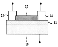
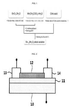
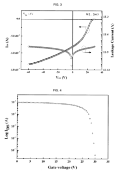
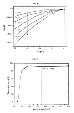
- A p-type transparent oxide semiconductor with a tin oxide compound (Sn1-xMxO2) doped with tri-valent metals like Rh, Al, Mn, Fe, Co, Cr, or Ga, which can be synthesized using a sol-gel method with a rutile structure, enabling lower temperature heat treatment and improved carrier mobility and light transmittance.
Environmental Impact and Sustainability Considerations
The environmental footprint of oxide semiconductor materials in transparent electronics represents a critical consideration in the industry's sustainable development. Traditional semiconductor manufacturing processes often involve toxic chemicals, high energy consumption, and rare earth elements that pose significant environmental challenges. In contrast, oxide semiconductors such as IGZO (Indium Gallium Zinc Oxide) can be fabricated using relatively lower temperature processes, reducing energy requirements by up to 30% compared to conventional silicon-based technologies.
Material selection plays a pivotal role in environmental sustainability. While indium remains a key component in many oxide semiconductors, its limited global supply raises concerns about resource depletion. Recent research has focused on developing alternative compositions that reduce or eliminate dependence on scarce elements. Zinc-tin oxide and aluminum-doped zinc oxide systems have emerged as promising candidates with reduced environmental impact while maintaining acceptable electrical performance.
Manufacturing processes for oxide semiconductors have evolved toward more environmentally friendly approaches. Solution-based deposition methods, including sol-gel and spin coating techniques, significantly reduce chemical waste compared to vacuum-based processes. Additionally, these methods typically operate at temperatures below 500°C, further decreasing the carbon footprint of device fabrication. Life cycle assessments indicate that solution-processed oxide semiconductors can reduce greenhouse gas emissions by up to 45% compared to conventional vacuum deposition techniques.
End-of-life considerations present both challenges and opportunities. The integration of oxide semiconductors in transparent electronics creates complex material systems that can be difficult to separate and recycle. However, the inherent stability of metal oxides may extend device lifespans, reducing electronic waste generation. Emerging recycling technologies specifically designed for oxide-based electronics show potential for recovering up to 80% of valuable materials, though commercial implementation remains limited.
Water usage represents another significant environmental factor. Traditional semiconductor manufacturing can consume thousands of liters of ultra-pure water per wafer. Oxide semiconductor processes typically require 40-60% less water, particularly when employing solution-based fabrication methods. Several research groups have demonstrated closed-loop water recycling systems specifically optimized for oxide semiconductor production, further reducing the water footprint.
Regulatory frameworks increasingly influence material selection and processing choices. The European Union's Restriction of Hazardous Substances (RoHS) directive and similar regulations worldwide have accelerated the transition toward environmentally benign materials and processes in transparent electronics. Industry leaders have responded by establishing sustainability metrics specifically for oxide semiconductor technologies, creating standardized environmental impact assessment methodologies that facilitate meaningful comparisons between competing material systems.
Manufacturing Scalability and Cost Analysis
The scalability of oxide semiconductor manufacturing processes represents a critical factor in the widespread adoption of transparent electronics. Current production methods for high-quality oxide semiconductors, particularly indium gallium zinc oxide (IGZO), involve sophisticated physical vapor deposition techniques such as sputtering and pulsed laser deposition. While these methods yield excellent material properties, they face significant challenges when scaled to mass production levels, particularly regarding uniformity across large substrates and throughput limitations.
Cost analysis reveals that material expenses constitute approximately 30-40% of total production costs for oxide semiconductor-based devices. Indium, a key component in many high-performance oxide semiconductors, presents particular concerns due to its limited global supply and price volatility. Recent market data indicates indium prices fluctuating between $200-350/kg over the past five years, creating uncertainty in long-term cost projections for manufacturers.
Solution-based processing methods, including sol-gel and chemical bath deposition, offer promising alternatives for cost reduction, with potential manufacturing cost savings of 40-60% compared to vacuum-based techniques. However, these methods currently struggle to achieve the same level of performance consistency as vacuum deposition processes, particularly regarding carrier mobility and threshold voltage stability.
Roll-to-roll manufacturing compatibility represents another crucial aspect of scalability for transparent electronics. Recent advancements in low-temperature processing have enabled deposition on flexible substrates at temperatures below 200°C, opening pathways for continuous production methods. Industry analysis suggests that successful implementation of roll-to-roll manufacturing could reduce production costs by up to 70% while increasing throughput by an order of magnitude.
Equipment depreciation and maintenance costs also significantly impact the economic viability of oxide semiconductor production. Vacuum-based systems require substantial capital investment ($1-5 million per production line) and ongoing maintenance expenses. Emerging atmospheric pressure spatial atomic layer deposition (AP-SALD) techniques show promise in reducing these capital costs by 40-60% while maintaining material quality comparable to conventional methods.
Yield rates present another critical economic factor, with current industrial processes achieving approximately 80-90% yield for small-to-medium sized displays. Defect density reduction remains a primary challenge, particularly for large-area applications. Recent research indicates that optimized process parameters and in-line quality monitoring systems can potentially increase yields to 95%, significantly improving cost-effectiveness for mass production scenarios.
Unlock deeper insights with PatSnap Eureka Quick Research — get a full tech report to explore trends and direct your research. Try now!
Generate Your Research Report Instantly with AI Agent
Supercharge your innovation with PatSnap Eureka AI Agent Platform!