Comparison of Oxide Semiconductor Conductivity with Metal Oxides
SEP 25, 20259 MIN READ
Generate Your Research Report Instantly with AI Agent
Patsnap Eureka helps you evaluate technical feasibility & market potential.
Oxide Semiconductor Conductivity Background and Objectives
Oxide semiconductors have emerged as a significant class of materials in the field of electronics and optoelectronics over the past several decades. The evolution of these materials can be traced back to the 1960s when initial research on zinc oxide (ZnO) and tin oxide (SnO2) began to reveal their unique semiconductor properties. However, it wasn't until the early 2000s that oxide semiconductors gained substantial attention with the development of transparent conducting oxides (TCOs) and the subsequent discovery of amorphous oxide semiconductors (AOS).
The technological trajectory of oxide semiconductors has been marked by continuous improvements in material synthesis, characterization techniques, and device fabrication processes. From the initial focus on binary oxides like ZnO and In2O3, the field has expanded to include more complex multicomponent systems such as InGaZnO (IGZO) and ZnSnO (ZTO), which offer enhanced electrical performance and stability.
A fundamental aspect that distinguishes oxide semiconductors from conventional metal oxides is their conductivity mechanism. While metal oxides typically exhibit insulating or highly resistive behavior due to their large bandgaps and localized electron states, oxide semiconductors possess unique electronic structures that enable moderate to high conductivity. This distinction arises from the specific orbital configurations and overlaps that facilitate electron mobility despite the presence of oxygen atoms, which traditionally act as electron traps.
The primary objective of studying oxide semiconductor conductivity in comparison with metal oxides is to establish a comprehensive understanding of the electronic transport mechanisms that govern their behavior. This includes investigating the roles of oxygen vacancies, cation defects, and band structure in determining conductivity. Additionally, the research aims to identify optimal compositional and structural parameters that can enhance conductivity while maintaining other desirable properties such as optical transparency and environmental stability.
From an application perspective, the goal is to develop oxide semiconductor materials with tailored conductivity profiles suitable for various electronic applications, ranging from thin-film transistors (TFTs) and transparent electrodes to gas sensors and photovoltaic devices. The ability to precisely control conductivity through doping, annealing, and compositional engineering represents a key technological target in this field.
Current research trends indicate a growing interest in exploring novel oxide semiconductor compositions, particularly those based on earth-abundant and environmentally friendly elements, as alternatives to indium-based materials which face supply constraints. Furthermore, there is an increasing focus on understanding and exploiting the unique advantages of amorphous oxide semiconductors, which offer uniform properties over large areas and compatibility with flexible substrates.
Market Applications and Demand Analysis
The global market for oxide semiconductors has witnessed substantial growth in recent years, driven primarily by the expanding electronics industry and increasing demand for high-performance display technologies. The market size for oxide semiconductor materials reached approximately $3.2 billion in 2022 and is projected to grow at a CAGR of 12.5% through 2028, reflecting the rising adoption across multiple application domains.
The display industry represents the largest application segment for oxide semiconductors, particularly for thin-film transistors (TFTs) in flat panel displays. IGZO (Indium Gallium Zinc Oxide) has emerged as the dominant material in this sector due to its superior electron mobility compared to traditional amorphous silicon. Major display manufacturers have increasingly incorporated IGZO-based TFTs in premium OLED and LCD panels, enhancing resolution while reducing power consumption.
Consumer electronics constitutes another significant market segment, with oxide semiconductors finding applications in smartphones, tablets, and wearable devices. The demand is primarily driven by the need for higher performance, lower power consumption, and thinner form factors. Apple's adoption of IGZO displays in iPads marked a pivotal moment for market expansion, demonstrating the commercial viability of this technology in high-volume consumer products.
The automotive sector represents a rapidly growing application area, particularly for transparent conductive oxides in smart windows, heads-up displays, and touch panels. As vehicles become more electrified and digitalized, the demand for advanced display technologies and sensors incorporating oxide semiconductors is expected to surge, with projections indicating a market growth of 15% annually in this segment.
Photovoltaics and energy harvesting applications have also begun to leverage the unique properties of oxide semiconductors. Transparent conducting oxides like ITO (Indium Tin Oxide) and FTO (Fluorine-doped Tin Oxide) are essential components in solar cells, while emerging research explores zinc oxide and titanium dioxide for next-generation photovoltaic technologies.
Healthcare and medical devices represent an emerging application area with significant potential. Transparent and flexible oxide semiconductor-based sensors are being developed for wearable health monitoring devices, point-of-care diagnostics, and biomedical imaging. This segment is expected to grow substantially as healthcare continues its digital transformation.
Regional analysis indicates that Asia-Pacific dominates the market, accounting for over 60% of global demand, primarily due to the concentration of display manufacturing and electronics production in countries like South Korea, Japan, China, and Taiwan. North America and Europe follow, with growing applications in specialized sectors including aerospace, defense, and advanced medical technologies.
Current State and Technical Challenges
Oxide semiconductor technology has evolved significantly over the past two decades, with substantial advancements in understanding their conductivity mechanisms compared to traditional metal oxides. Currently, the field is dominated by several key oxide semiconductor materials including indium gallium zinc oxide (IGZO), zinc tin oxide (ZTO), and zinc oxide (ZnO), each exhibiting unique conductivity characteristics that differentiate them from conventional metal oxides like titanium dioxide (TiO2) and aluminum oxide (Al2O3).
The global research landscape shows concentration of expertise in East Asia, particularly Japan, South Korea, and Taiwan, where major display manufacturers have invested heavily in oxide semiconductor research. European research institutions focus more on fundamental physics of these materials, while North American efforts are primarily directed toward novel applications beyond display technologies.
A significant technical challenge in this field remains the stability of conductivity under various environmental conditions. Unlike metals with their free electron model, oxide semiconductors exhibit complex carrier transport mechanisms that are highly sensitive to oxygen vacancies and structural defects. Recent studies indicate that humidity, temperature fluctuations, and prolonged light exposure can significantly alter the conductivity profiles of many oxide semiconductors, creating reliability issues for commercial applications.
Another critical challenge is the trade-off between transparency and conductivity. While metal oxides typically sacrifice optical transparency as conductivity increases, oxide semiconductors must maintain both properties simultaneously for many applications. This fundamental materials science challenge has prompted extensive research into band structure engineering and doping strategies.
The scalability of manufacturing processes presents another significant hurdle. Current deposition techniques for high-quality oxide semiconductor films include sputtering, pulsed laser deposition, and solution processing methods. However, achieving uniform electrical properties across large-area substrates remains problematic, with edge effects and compositional variations leading to inconsistent conductivity profiles.
Computational modeling of oxide semiconductor conductivity has advanced substantially but still lacks the predictive power achieved in silicon-based semiconductor modeling. The complex interplay between structural defects, oxygen stoichiometry, and electronic properties creates significant challenges for accurate simulation of these materials' behavior under operating conditions.
Recent breakthroughs in characterization techniques, particularly in-situ transmission electron microscopy combined with electrical measurements, have provided unprecedented insights into the dynamic nature of conductivity in these materials. These advances have revealed that the metal-semiconductor interface plays a more critical role than previously understood, with band alignment and contact resistance significantly influencing overall device performance.
Current Conductivity Enhancement Solutions
01 Doping and composition control for conductivity enhancement
Controlling the conductivity of oxide semiconductors and metal oxides through doping with specific elements or adjusting their composition. This approach involves introducing impurities or modifying the stoichiometry to create charge carriers, thereby enhancing electrical conductivity. Various dopants such as transition metals, rare earth elements, or non-metals can be incorporated to tune the electronic properties of the oxide materials for specific applications in electronics and optoelectronics.- Doping strategies for controlling oxide semiconductor conductivity: Doping is a key strategy for modifying the electrical conductivity of oxide semiconductors. By introducing specific impurities into the crystal structure, the carrier concentration and mobility can be precisely controlled. Various dopants such as metals, non-metals, and rare earth elements can be used to create n-type or p-type semiconductors with tailored conductivity properties. The doping concentration and distribution significantly impact the resulting electronic properties, allowing for customization of oxide semiconductors for specific applications.
- Thin film deposition techniques for oxide semiconductor fabrication: Various deposition techniques are employed to fabricate oxide semiconductor thin films with controlled conductivity. Methods include physical vapor deposition (PVD), chemical vapor deposition (CVD), atomic layer deposition (ALD), and solution-based processes. The deposition parameters such as temperature, pressure, and precursor composition significantly influence the microstructure, stoichiometry, and defect concentration in the resulting films, which in turn affect their electrical conductivity. Post-deposition treatments like annealing can further modify the conductivity by altering the crystal structure and oxygen vacancy concentration.
- Oxygen vacancy engineering in metal oxides: Oxygen vacancies play a crucial role in determining the conductivity of metal oxide semiconductors. These point defects act as electron donors, significantly increasing the carrier concentration and thus the conductivity. The concentration of oxygen vacancies can be controlled through processing conditions such as annealing in reducing or oxidizing atmospheres, controlling oxygen partial pressure during synthesis, or through electrochemical methods. By precisely engineering oxygen vacancy concentration, the electrical properties of metal oxides can be tuned from insulating to highly conductive states.
- Nanostructured metal oxides for enhanced conductivity: Nanostructuring of metal oxides offers a pathway to enhance their electrical conductivity. By creating nanoscale architectures such as nanoparticles, nanowires, nanotubes, or nanosheets, the surface-to-volume ratio increases dramatically, altering the electronic band structure and charge carrier transport mechanisms. Quantum confinement effects in nanoscale dimensions can modify the bandgap and carrier mobility. Additionally, the increased grain boundary density in nanostructured materials can either enhance or impede conductivity depending on the specific material system and processing conditions.
- Composite and heterojunction oxide semiconductor systems: Composite materials combining different metal oxides or metal oxides with other materials can exhibit unique conductivity characteristics. These heterogeneous systems often display synergistic effects where the overall conductivity exceeds that of the individual components. Interfaces between dissimilar materials create band bending and charge transfer, leading to the formation of conductive channels. Multilayer structures and heterojunctions can be designed to control carrier transport pathways. These composite approaches enable the development of oxide semiconductor systems with tailored conductivity profiles for specific electronic applications.
02 Thin film deposition techniques for oxide semiconductors
Methods for depositing thin films of oxide semiconductors and metal oxides with controlled conductivity properties. These techniques include physical vapor deposition, chemical vapor deposition, atomic layer deposition, and solution-based processes. The deposition parameters significantly influence the crystallinity, microstructure, and interfacial properties of the oxide films, which in turn affect their electrical conductivity and performance in electronic devices such as thin-film transistors and transparent conductive electrodes.Expand Specific Solutions03 Post-treatment processes to modify oxide conductivity
Various post-deposition treatments to modify and enhance the conductivity of oxide semiconductors and metal oxides. These processes include thermal annealing in different atmospheres, plasma treatments, laser processing, and chemical treatments. Such post-treatments can modify the oxygen vacancy concentration, crystalline structure, and defect states in the oxide materials, thereby tailoring their electrical properties for specific applications in sensors, catalysts, and electronic components.Expand Specific Solutions04 Novel oxide semiconductor compositions and structures
Development of novel oxide semiconductor materials and composite structures with enhanced or tunable conductivity. These include multi-component oxides, nanostructured oxides, and heterostructures combining different oxide materials. The innovative compositions and structures enable precise control over electronic properties, leading to improved performance in applications such as gas sensors, photocatalysts, energy storage devices, and next-generation electronic components.Expand Specific Solutions05 Measurement and characterization of oxide conductivity
Methods and systems for measuring and characterizing the electrical conductivity of oxide semiconductors and metal oxides. These techniques include impedance spectroscopy, Hall effect measurements, four-point probe testing, and temperature-dependent conductivity analysis. Advanced characterization approaches help understand the fundamental mechanisms governing charge transport in oxide materials, enabling the development of materials with optimized conductivity properties for various technological applications.Expand Specific Solutions
Key Industry Players and Competition Landscape
The oxide semiconductor conductivity market is in a growth phase, with increasing applications in display technologies and power electronics. The market is expanding due to demand for high-performance, energy-efficient devices, with a projected CAGR of 12% through 2025. Technologically, metal oxide semiconductors are advancing rapidly, with companies at different maturity levels. Samsung Electronics and TSMC lead with commercial production capabilities, while Semiconductor Energy Laboratory specializes in IGZO technology. Tianma Microelectronics and CEC-PANDA focus on display applications, with research institutions like UCLouvain and Peking University driving fundamental innovations. Toshiba and Ricoh are developing specialized applications, creating a competitive landscape balanced between established manufacturers and emerging research-driven entities.
Semiconductor Energy Laboratory Co., Ltd.
Technical Solution: Semiconductor Energy Laboratory (SEL) has pioneered advanced oxide semiconductor technology, particularly focusing on IGZO (Indium Gallium Zinc Oxide) semiconductors. Their proprietary c-axis aligned crystalline IGZO (CAAC-IGZO) technology demonstrates superior conductivity characteristics compared to conventional metal oxides. SEL's research has shown that CAAC-IGZO exhibits electron mobility of 10-100 cm²/Vs, significantly higher than amorphous silicon (0.5-1 cm²/Vs) while maintaining lower off-state current. Their technology enables precise control of oxygen vacancy concentration, which directly affects carrier concentration and conductivity. SEL has developed specialized deposition techniques that create highly ordered crystalline structures while maintaining the advantages of amorphous materials, resulting in stable electrical properties even under environmental stress conditions like temperature fluctuation and light exposure.
Strengths: Superior stability against environmental stressors compared to other oxide semiconductors; excellent scalability for large-area electronics; compatibility with low-temperature processing. Weaknesses: Higher manufacturing complexity than conventional metal oxides; requires precise control of deposition parameters; higher material costs due to indium content.
Samsung Electronics Co., Ltd.
Technical Solution: Samsung Electronics has developed proprietary oxide semiconductor technology focusing on optimizing conductivity for display applications. Their research compares various metal oxide compositions, particularly focusing on IGZO and zinc tin oxide (ZTO) systems. Samsung's approach involves precise control of oxygen partial pressure during sputtering deposition to manipulate carrier concentration and mobility. Their comparative studies have demonstrated that optimized ZTO can achieve conductivity values of 10^2-10^3 S/cm, approaching some metallic conductors while maintaining semiconductor properties. Samsung has pioneered the implementation of oxide semiconductors in commercial display products, developing specialized annealing processes that enhance crystallinity while maintaining low processing temperatures compatible with flexible substrates. Their technology enables precise modulation of the metal-to-oxygen ratio, directly affecting band structure and conductivity properties.
Strengths: Extensive manufacturing infrastructure allowing rapid commercialization; excellent integration with existing display technologies; demonstrated reliability in consumer products. Weaknesses: Proprietary formulations limit academic collaboration; primarily focused on display applications rather than broader semiconductor applications.
Critical Patents and Research in Oxide Semiconductors
Method of producing metal oxides with increased electrical conductivity
PatentActiveUS11739438B2
Innovation
- A method involving modulated annealing, where single crystal oxides are alternately exposed to nitrogen and oxygen gases at controlled temperatures to increase conductivity, altering the bulk and surface electronic properties by modifying the number of accessible bonding states.
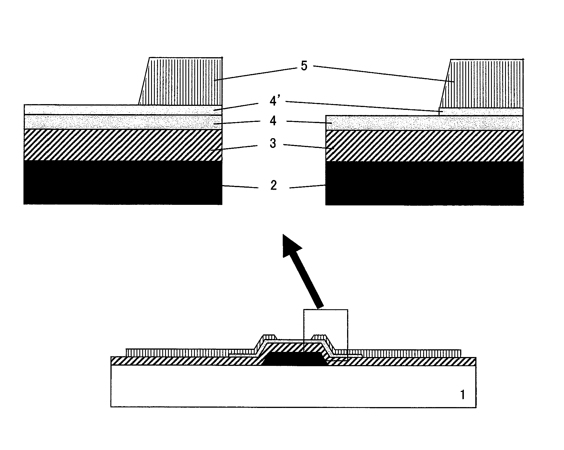
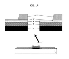
Oxide semiconductor device with oxide semiconductor layers of different oxygen concentrations and method of manufacturing the same
PatentInactiveUS8368067B2
Innovation
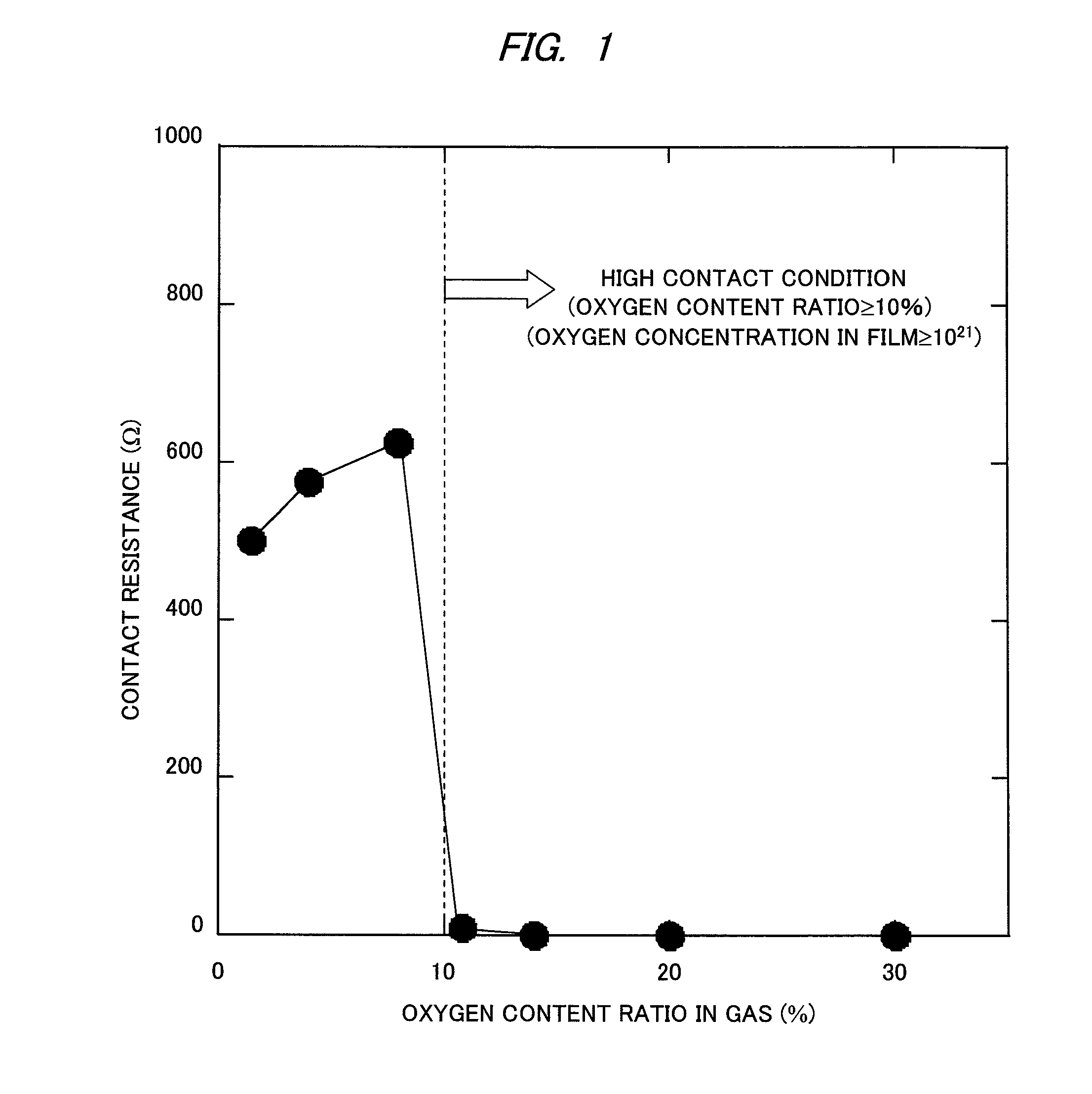
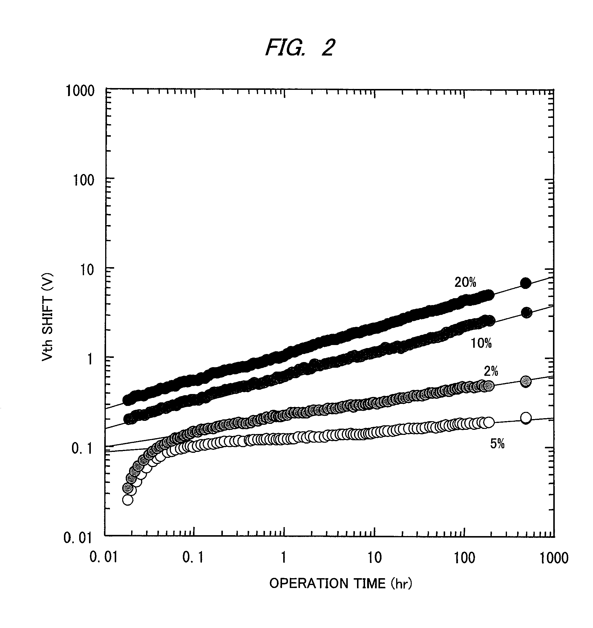
- A multilayered structure is implemented with an oxide semiconductor layer having a low oxygen content ratio near the gate insulating film and a high oxygen content ratio near the metal electrode, optimizing oxygen concentrations to balance contact resistance and threshold potential shift, ensuring effective ohmic contact and reliability.
Material Sustainability and Environmental Impact
The sustainability profile of oxide semiconductors presents significant environmental advantages compared to traditional metal oxide materials. Oxide semiconductors typically require lower processing temperatures and fewer toxic precursors during manufacturing, resulting in reduced energy consumption and carbon footprint. For instance, amorphous indium-gallium-zinc oxide (IGZO) can be processed at temperatures below 300°C, whereas conventional silicon-based semiconductors often require temperatures exceeding 1000°C.
Material extraction considerations reveal important distinctions between oxide semiconductors and metal oxides. While both rely on metal extraction processes with environmental impacts, oxide semiconductors often utilize smaller quantities of rare elements. However, indium, a common component in transparent oxide semiconductors, faces supply constraints and geopolitical challenges that may affect long-term sustainability.
Life cycle assessment (LCA) studies demonstrate that oxide semiconductor devices generally exhibit lower environmental impact scores across multiple categories including global warming potential, acidification, and resource depletion. This advantage stems primarily from their reduced energy requirements during manufacturing and extended operational lifetimes compared to conventional metal oxide alternatives.
Recyclability represents another critical sustainability factor. Oxide semiconductor devices typically contain fewer toxic components than traditional electronics, facilitating end-of-life processing. However, the complex integration of these materials into multilayer electronic structures continues to present recycling challenges that require innovative separation techniques and recovery processes.
Water consumption during manufacturing deserves particular attention, as semiconductor fabrication traditionally demands significant ultrapure water resources. Oxide semiconductor production processes have demonstrated potential for reduced water intensity, with some manufacturing techniques requiring up to 30% less water than conventional metal oxide processing.
Emerging research in bio-compatible and biodegradable oxide semiconductors offers promising pathways toward truly sustainable electronics. Recent developments in zinc oxide and iron oxide-based semiconductors derived from sustainable precursors demonstrate the potential for environmentally benign electronic materials with minimal ecological footprint throughout their lifecycle.
Regulatory frameworks worldwide increasingly emphasize materials sustainability, with directives like the European Union's Restriction of Hazardous Substances (RoHS) and Registration, Evaluation, Authorization and Restriction of Chemicals (REACH) influencing material selection. Oxide semiconductors generally align well with these regulatory trends, positioning them favorably for future market adoption as sustainability requirements intensify across global supply chains.
Manufacturing Scalability and Cost Analysis
The manufacturing scalability of oxide semiconductors presents significant advantages over traditional silicon-based technologies, particularly in large-area electronics applications. Oxide semiconductors can be deposited using relatively low-temperature processes (typically below 400°C), enabling compatibility with a wide range of substrates including flexible polymers. This temperature advantage translates directly to reduced energy consumption and processing costs compared to silicon technologies requiring high-temperature processing (>1000°C).
From a capital expenditure perspective, oxide semiconductor manufacturing facilities require substantially lower investment than silicon fabs. While a modern silicon semiconductor fab may cost $10-20 billion, facilities for oxide semiconductor production can be established for a fraction of this amount, often in the hundreds of millions range. This lower barrier to entry has allowed more manufacturers to enter the market, particularly in regions with developing economies.
Material costs for oxide semiconductors vary significantly based on composition. Indium-containing compounds (like IGZO) face supply chain challenges due to indium's relative scarcity and price volatility. Recent market data indicates indium prices fluctuating between $200-500/kg, impacting production economics. Alternative zinc-tin oxide formulations offer more stable supply chains with raw material costs approximately 30-40% lower than indium-based alternatives.
Deposition techniques significantly impact both scalability and cost structures. Sputtering remains the dominant industrial method, offering excellent uniformity across large substrates with material utilization efficiency of 40-60%. Solution processing methods (spin-coating, inkjet printing) demonstrate promising cost reductions in R&D settings but face challenges in achieving consistent electrical properties at industrial scales. Recent advances in spatial atomic layer deposition show potential for combining high-quality film formation with improved throughput.
Yield considerations remain critical to manufacturing economics. Current industrial processes for oxide semiconductors achieve yields of 85-95% for display applications, comparing favorably to early implementation stages but still trailing mature silicon technologies. Defect densities typically range from 0.1-1.0 defects/cm², with primary failure modes relating to compositional non-uniformity and interface quality issues.
When comparing total production costs, oxide semiconductor TFT backplanes demonstrate a 30-50% cost advantage over LTPS (Low-Temperature Polysilicon) alternatives for large-area applications, while maintaining adequate performance for most consumer electronics applications. This cost advantage has been instrumental in enabling the rapid market penetration of oxide semiconductor technologies in display applications and positions them favorably for emerging flexible electronics markets.
Unlock deeper insights with Patsnap Eureka Quick Research — get a full tech report to explore trends and direct your research. Try now!
Generate Your Research Report Instantly with AI Agent
Supercharge your innovation with Patsnap Eureka AI Agent Platform!