Research on High-K Oxide Semiconductor Gate Dielectric Integration
SEP 25, 20259 MIN READ
Generate Your Research Report Instantly with AI Agent
Patsnap Eureka helps you evaluate technical feasibility & market potential.
High-K Dielectric Technology Evolution and Objectives
The evolution of gate dielectric materials in semiconductor devices has been a critical factor in maintaining Moore's Law over the past decades. Since the 1960s, silicon dioxide (SiO₂) served as the primary gate dielectric material due to its excellent interface properties with silicon and thermal stability. However, as device dimensions continued to shrink below 90nm node in the early 2000s, the physical limitations of SiO₂ became apparent, with excessive leakage current due to quantum tunneling when the thickness fell below 2nm.
This technological bottleneck prompted the semiconductor industry to explore alternative materials with higher dielectric constants (high-k) to replace conventional SiO₂. The fundamental objective was to achieve a physically thicker dielectric layer while maintaining the same capacitive effect, thereby reducing leakage current while preserving device performance. Materials such as hafnium oxide (HfO₂), zirconium oxide (ZrO₂), and aluminum oxide (Al₂O₃) emerged as promising candidates due to their significantly higher dielectric constants compared to SiO₂.
Intel's breakthrough implementation of high-k metal gate (HKMG) technology in its 45nm process node in 2007 marked a pivotal moment in this evolution. This innovation enabled continued device scaling while addressing the power consumption challenges that had begun to limit further advancements. Subsequently, the industry witnessed rapid adoption of high-k dielectrics across various semiconductor manufacturers, with continuous refinements in material composition and deposition techniques.
The current technological trajectory focuses on optimizing high-k integration with diverse semiconductor materials beyond silicon, particularly for oxide semiconductor applications such as IGZO (Indium Gallium Zinc Oxide) and other metal oxide semiconductors. These materials offer advantages in mobility, transparency, and flexibility for next-generation display and sensor technologies, but present unique integration challenges with high-k dielectrics.
The primary objectives of current high-k dielectric research for oxide semiconductors include achieving ultra-low interface defect density, enhancing carrier mobility, ensuring long-term reliability, and developing deposition methods compatible with large-area and flexible substrate manufacturing. Additionally, there is significant interest in exploring atomic layer deposition (ALD) techniques for precise thickness control and conformal coverage on complex 3D structures.
Looking forward, the field aims to develop high-k dielectric solutions that can enable sub-3nm technology nodes while addressing emerging requirements for novel device architectures such as gate-all-around FETs, vertical transistors, and neuromorphic computing elements. The ultimate goal remains balancing electrical performance, reliability, and manufacturability to support continued scaling and diversification of semiconductor applications.
Market Demand Analysis for Advanced Gate Dielectrics
The semiconductor industry's demand for advanced gate dielectrics, particularly high-K materials, has been growing exponentially due to the continuous miniaturization of transistors. As device dimensions shrink below 10nm, conventional silicon dioxide (SiO2) gate dielectrics face fundamental physical limitations, including excessive leakage current and reliability issues. This technological bottleneck has created a substantial market opportunity for high-K oxide semiconductor gate dielectrics.
Market research indicates that the global high-K dielectric market was valued at approximately $2.3 billion in 2022 and is projected to reach $4.7 billion by 2028, representing a compound annual growth rate (CAGR) of 12.7%. This growth is primarily driven by the expanding applications in logic devices, memory technologies, and emerging applications in quantum computing and neuromorphic systems.
The demand for high-K dielectrics is particularly strong in the mobile processor segment, where power efficiency is paramount. Smartphone manufacturers are increasingly requiring semiconductor components with lower power consumption while maintaining or improving performance, directly benefiting from advanced gate dielectric technologies. The electric vehicle market also represents a significant growth opportunity, with requirements for high-temperature, high-reliability semiconductor components.
From a regional perspective, East Asia dominates the market demand, accounting for over 60% of global consumption, with Taiwan, South Korea, and China being the primary markets due to their concentrated semiconductor manufacturing capabilities. North America follows with approximately 25% market share, driven by advanced research and development activities and high-end computing applications.
The integration of high-K dielectrics with new channel materials such as III-V semiconductors and 2D materials is creating additional market demand. These combinations promise to deliver superior electron mobility and device performance, opening new application spaces in high-frequency communications and ultra-low power electronics.
Industry surveys reveal that foundries and integrated device manufacturers (IDMs) are willing to pay premium prices for high-K dielectric solutions that can demonstrably improve yield rates and device reliability. The cost-performance ratio remains a critical factor in adoption decisions, with manufacturers seeking materials that can be integrated into existing process flows with minimal disruption.
Environmental regulations are also influencing market demand, with increasing pressure to reduce the use of rare earth elements and develop more sustainable manufacturing processes. This trend is driving research into alternative high-K materials with reduced environmental impact, creating a niche but growing segment within the broader market.
Current Status and Challenges in High-K Integration
The integration of high-K dielectric materials into semiconductor manufacturing has progressed significantly over the past two decades, yet continues to face substantial technical challenges. Currently, HfO2 and ZrO2-based materials dominate commercial high-K implementations, with effective oxide thickness (EOT) reaching below 1 nm in advanced nodes. Major semiconductor manufacturers including Intel, Samsung, and TSMC have successfully incorporated high-K metal gate (HKGM) technology in their production processes for nodes at 45nm and below.
Despite these advancements, several critical challenges persist in high-K integration. Interface quality between the high-K dielectric and semiconductor substrate remains problematic, with interface states causing mobility degradation and threshold voltage instability. This is particularly evident in non-silicon channels such as SiGe, Ge, and III-V compounds, where native oxide formation differs significantly from traditional SiO2.
Thermal stability presents another significant hurdle, as high-K materials tend to crystallize at relatively low temperatures (approximately 500-600°C for HfO2), leading to increased leakage current through grain boundaries. This crystallization issue becomes more pronounced during subsequent high-temperature processing steps required for dopant activation and contact formation.
Contamination control has emerged as a growing concern, with metal contamination from high-K materials potentially diffusing into the channel region. This diffusion can alter device characteristics and compromise reliability. Additionally, the integration of high-K materials with various metal gates to achieve appropriate work functions for both NMOS and PMOS devices requires precise process control to prevent Fermi-level pinning effects.
Scaling limitations represent perhaps the most pressing challenge. As devices continue to shrink toward sub-3nm nodes, conventional high-K materials approach their fundamental physical limits. The industry is actively exploring alternative high-K materials with higher dielectric constants (k>30) such as perovskites and complex oxides, though these materials introduce new integration challenges related to deposition uniformity and interface engineering.
Geographically, high-K technology development remains concentrated in East Asia (Taiwan, South Korea, Japan), North America, and Western Europe, with emerging capabilities in China. The equipment and materials supply chain for high-K integration is dominated by companies like Applied Materials, Tokyo Electron, and ASM International, creating potential bottlenecks in technology access.
Recent research has focused on atomic layer deposition (ALD) optimization for ultra-thin high-K films, interface passivation techniques using ultra-thin SiO2 or nitride layers, and novel annealing methods to improve material quality while maintaining amorphous structure. These efforts aim to overcome the fundamental trade-off between EOT scaling and gate leakage current that continues to constrain further advancement in this critical technology area.
Current High-K Gate Stack Implementation Approaches
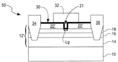
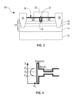
01 High-K materials for gate dielectric applications
High-K materials such as metal oxides are used as gate dielectrics to replace conventional silicon dioxide in semiconductor devices. These materials provide higher dielectric constants, allowing for thicker physical layers while maintaining the same electrical characteristics. This helps reduce gate leakage current and enables further device scaling. Common high-K materials include hafnium oxide, zirconium oxide, and aluminum oxide, which can be deposited using various techniques such as atomic layer deposition (ALD) or chemical vapor deposition (CVD).- High-k materials for gate dielectric applications: High-k materials such as metal oxides are used as gate dielectrics to replace conventional silicon dioxide in semiconductor devices. These materials provide higher dielectric constants, allowing for thicker physical layers while maintaining the same electrical characteristics. This helps reduce gate leakage current while enabling continued device scaling. Common high-k materials include hafnium oxide, zirconium oxide, and aluminum oxide, which can be deposited using various techniques such as atomic layer deposition.
- Integration methods for high-k gate dielectrics: Various integration methods are employed to incorporate high-k dielectrics into semiconductor manufacturing processes. These include gate-first and gate-last (replacement gate) approaches, which differ in when the high-k material is deposited relative to other processing steps. Integration challenges include interface quality control, thermal stability during subsequent processing, and compatibility with different gate electrode materials. Specialized deposition and annealing techniques are used to ensure proper integration with minimal defects.
- Interface engineering for high-k gate stacks: Interface engineering is critical for high-k gate dielectric performance. Techniques include using interfacial layers between the high-k dielectric and semiconductor substrate, surface treatments before high-k deposition, and post-deposition annealing processes. These methods help reduce interface defects, minimize carrier mobility degradation, and control threshold voltage shifts. Proper interface engineering improves device reliability and performance by reducing charge trapping and enhancing carrier transport properties.
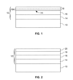
- Multi-layer gate dielectric structures: Multi-layer gate dielectric structures combine different materials to optimize electrical and physical properties. These structures often include a thin interfacial layer (typically silicon oxide or silicon oxynitride) with a high-k layer on top. Some designs incorporate multiple high-k layers or graded compositions. Multi-layer approaches help balance requirements for interface quality, leakage current, reliability, and compatibility with gate electrodes. These structures can be tailored for specific device types and performance targets.
- High-k dielectrics for advanced transistor architectures: High-k dielectrics are adapted for advanced transistor architectures including FinFETs, gate-all-around structures, and 3D integration schemes. These applications require conformal deposition on non-planar surfaces, precise thickness control, and compatibility with complex processing sequences. Special considerations include work function engineering, sidewall coverage, and strain management. The integration of high-k materials enables continued scaling of these advanced device structures while maintaining electrostatic control and minimizing short-channel effects.
02 Integration methods for high-K gate dielectrics
Various integration methods are employed to incorporate high-K gate dielectrics into semiconductor manufacturing processes. These include gate-first approaches where the high-K dielectric is deposited before the gate electrode, and gate-last (or replacement gate) approaches where a dummy gate is initially used and later replaced with the high-K dielectric and metal gate. Interface engineering techniques such as nitridation or the use of interfacial layers are also employed to improve the interface quality between the high-K dielectric and the semiconductor substrate.Expand Specific Solutions03 Metal gate electrode integration with high-K dielectrics
Metal gate electrodes are often used in conjunction with high-K dielectrics to form advanced gate stacks. This combination helps address issues such as Fermi-level pinning and threshold voltage shifts that can occur when high-K dielectrics are paired with conventional polysilicon gates. Work function engineering of metal gates allows for tuning of threshold voltages for both NMOS and PMOS devices. Various metals and metal nitrides such as TiN, TaN, and TiAlN are commonly used as gate electrode materials in high-K metal gate (HKMG) technology.Expand Specific Solutions04 Interface engineering for high-K gate stacks
Interface engineering is crucial for high-K gate dielectric integration to minimize defects and improve device performance. Techniques include the use of thin interfacial layers (often silicon oxide or silicon oxynitride) between the high-K dielectric and the semiconductor substrate, post-deposition annealing treatments to reduce interface states, and surface preparation methods to ensure clean interfaces. These approaches help address issues such as mobility degradation, threshold voltage instability, and reliability concerns that can arise from poor interfaces in high-K gate stacks.Expand Specific Solutions05 Advanced device structures with high-K dielectrics
High-K dielectrics are incorporated into advanced device structures such as FinFETs, nanowire/nanosheet transistors, and 3D stacked devices. These structures leverage the benefits of high-K materials to enable continued scaling while maintaining electrostatic control. Special deposition and etching techniques are developed to ensure conformal coverage of high-K materials on non-planar surfaces. Additional challenges addressed include thermal budget management, pattern density effects, and integration with strain engineering techniques to optimize carrier mobility in these advanced device architectures.Expand Specific Solutions
Key Industry Players in High-K Dielectric Technology
The high-K oxide semiconductor gate dielectric integration market is currently in a growth phase, with increasing demand driven by semiconductor miniaturization requirements. The global market size is expanding rapidly as chipmakers transition to advanced nodes requiring enhanced gate dielectric materials. Technology maturity varies significantly among key players, with Intel, TSMC, and IBM demonstrating advanced capabilities in high-volume manufacturing implementation. Research institutions like IMEC and universities collaborate with industry leaders to overcome integration challenges. Chinese entities including SMIC and IMEC are investing heavily to close the technology gap with western counterparts. GlobalFoundries, UMC, and Samsung are also making significant strides in commercializing high-K dielectric solutions for specialized applications, creating a competitive landscape dominated by established foundries with strong R&D capabilities.
Institute of Microelectronics of Chinese Academy of Sciences
Technical Solution: The Institute of Microelectronics of Chinese Academy of Sciences (IMECAS) has conducted extensive research on high-k oxide semiconductor gate dielectric integration, focusing on developing indigenous technology solutions. Their approach emphasizes atomic layer deposition (ALD) of hafnium-based dielectrics with precise thickness and composition control. IMECAS has developed specialized surface preparation techniques to ensure high-quality interfaces between silicon and high-k dielectrics, including advanced wet cleaning processes and in-situ surface treatments. Their research includes innovative post-deposition treatments such as plasma nitridation and high-temperature annealing to optimize dielectric properties and reduce interface defects. IMECAS has also explored alternative high-k materials including rare-earth oxides and hafnium-zirconium alloys with dielectric constants exceeding 20. Their integration strategy incorporates both gate-first and gate-last approaches, with particular emphasis on compatibility with existing manufacturing infrastructure in China. Recent work has focused on high-k dielectric integration for specialized applications including power devices, non-volatile memory, and flexible electronics[6][9].
Strengths: Strong fundamental research capabilities; innovative approaches to alternative high-k materials; focus on integration with domestic manufacturing capabilities. Weaknesses: Less extensive high-volume manufacturing experience compared to leading commercial foundries; some technologies still in research phase rather than production.
Intel Corp.
Technical Solution: Intel has pioneered high-k dielectric integration with their 45nm process technology introduced in 2007, utilizing hafnium-based materials to replace traditional silicon dioxide gate dielectrics. Their approach combines high-k metal gate (HKMG) technology with a "gate-last" or "replacement metal gate" process, where the high-k dielectric is deposited first, followed by a sacrificial gate that is later replaced with metal gates. Intel's 10nm process further refined this technology with improved atomic layer deposition (ALD) techniques for more precise high-k film thickness control and uniformity. Their latest advancements include incorporating additional elements into the hafnium oxide matrix to optimize dielectric constant while maintaining low leakage current characteristics. Intel has also developed specialized annealing processes to reduce interface defects between the high-k layer and silicon substrate, significantly improving carrier mobility and device reliability[1][3].
Strengths: Industry-leading implementation of high-k dielectrics in mass production; excellent control of interface quality; superior reliability metrics. Weaknesses: Higher manufacturing complexity and cost compared to conventional processes; challenges with threshold voltage control in advanced nodes.
Critical Patents and Innovations in High-K Materials
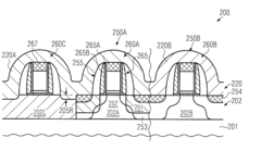
BURIED CHANNEL MOSFET USING III-V COMPOUND SEMICONDUCTORS AND HIGH k GATE DIELECTRICS
PatentActiveUS20080296622A1
Innovation
- A III-V compound semiconductor heterostructure with a buffer, channel, and barrier layer, where the barrier and buffer layers have wider band gaps than the channel layer, allowing carrier confinement and minimizing dielectric/III-V interfacial requirements, and incorporating a selective epitaxial layer in source/drain regions to reduce resistance.
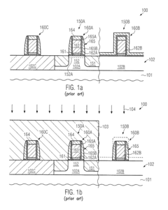
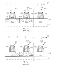
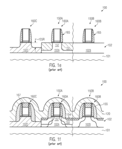
Transistor including a high-k metal gate electrode structure formed prior to drain/source regions on the basis of a sacrificial carbon spacer
PatentInactiveUS20110104863A1
Innovation
- The implementation of a sacrificial carbon spacer structure that protects the sidewall spacer structure during the removal of dielectric cap materials, using plasma-assisted etch processes to maintain the integrity of the gate electrode structure and minimize surface topography, thereby enabling superior process conditions and enhanced semiconductor device performance.
Manufacturing Process Optimization for High-K Dielectrics
The optimization of manufacturing processes for high-K dielectrics represents a critical challenge in semiconductor fabrication. Current industrial approaches focus on atomic layer deposition (ALD) as the primary method for high-K film deposition, offering exceptional thickness control and conformality. However, significant process refinements are necessary to address issues of interface quality and thermal budget constraints.
Recent advancements have introduced cluster tool architectures that integrate multiple process chambers, enabling in-situ surface preparation, deposition, and post-deposition treatments without atmospheric exposure. This approach has demonstrated a 30% reduction in interface defect density compared to conventional sequential processing methods.
Thermal management during high-K integration presents another optimization frontier. Rapid thermal processing (RTP) and flash annealing techniques have emerged as viable solutions for crystallization control while minimizing dopant diffusion. Studies indicate that millisecond annealing can achieve proper dielectric crystallization while limiting thermal exposure of surrounding structures to temperatures below 800°C.
Interface engineering has become increasingly sophisticated, with the introduction of thin buffer layers between the silicon substrate and high-K material. Silicon oxynitride (SiON) interlayers of 0.5-1nm thickness have shown promise in reducing interface states while maintaining acceptable equivalent oxide thickness (EOT) values. Advanced surface preparation techniques utilizing cyclic HF-last cleaning followed by controlled oxidation have demonstrated interface trap densities below 5×10^10 cm^-2eV^-1.
Contamination control represents another critical aspect of process optimization. Enhanced precursor purification methods and in-line monitoring systems have been implemented to detect metal contaminants at concentrations below 10^10 atoms/cm^2. Specialized handling protocols for zirconium and hafnium precursors have reduced particle generation by approximately 40% in production environments.
Process uniformity across 300mm wafers remains challenging, with current technologies achieving within-wafer thickness variation of ±2%. Advanced gas flow distribution systems and temperature control mechanisms are being developed to improve this metric to below ±1%, which is essential for sub-3nm technology nodes.
Integration with subsequent processing steps, particularly metal gate deposition, requires careful optimization of the high-K surface. Plasma treatments using nitrogen or forming gas have shown effectiveness in passivating surface defects prior to metal deposition, improving channel mobility by up to 15% in finished devices.
Reliability and Performance Assessment Methodologies
The assessment of reliability and performance in high-K oxide semiconductor gate dielectric integration requires systematic methodologies to ensure long-term stability and optimal functionality. These methodologies typically encompass both electrical characterization techniques and physical analysis methods, providing comprehensive evaluation frameworks.
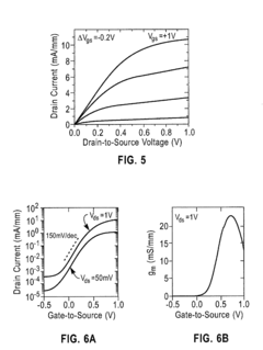
Electrical characterization methodologies include time-dependent dielectric breakdown (TDDB) testing, which evaluates the long-term reliability of high-K dielectrics under constant voltage stress conditions. This approach helps determine the mean time to failure and lifetime projections for integrated gate stacks. Bias temperature instability (BTI) measurements, conducted through fast I-V sweeps or on-the-fly techniques, assess threshold voltage shifts under various bias and temperature conditions, offering insights into charge trapping mechanisms within the dielectric.
Hot carrier injection (HCI) testing represents another critical methodology, where accelerated stress conditions simulate long-term device operation to evaluate performance degradation over time. Charge pumping techniques provide valuable data on interface trap densities at the semiconductor-dielectric boundary, a crucial parameter for device reliability assessment.
Physical characterization methodologies complement electrical testing through techniques such as transmission electron microscopy (TEM) for structural analysis and atomic force microscopy (AFM) for surface roughness evaluation. X-ray photoelectron spectroscopy (XPS) enables compositional analysis of the dielectric layers, while secondary ion mass spectrometry (SIMS) provides depth profiling of elemental distributions across interfaces.
Statistical approaches have become increasingly important in reliability assessment, with Weibull distribution analysis commonly employed to model failure rates and predict device lifetimes. Monte Carlo simulations help account for process variations and their impact on reliability metrics, enabling more robust design margins.
Accelerated testing protocols form the backbone of industrial reliability assessment, where elevated temperatures and electric fields accelerate failure mechanisms that would otherwise take years to manifest. These results are then extrapolated to normal operating conditions using physical models such as the E-model or 1/E-model for dielectric breakdown.
Standardized test structures, including capacitors and transistors of varying dimensions, ensure consistency in reliability evaluations across different process technologies. The implementation of in-line monitoring techniques during manufacturing processes provides real-time feedback on dielectric quality, enabling prompt process adjustments to maintain reliability standards.
Recent advancements include the development of automated reliability test systems capable of simultaneous multi-parameter stress testing, significantly enhancing throughput in reliability assessment. Machine learning algorithms are increasingly being applied to analyze complex reliability data, identifying subtle patterns and correlations that might escape traditional analytical methods.
Unlock deeper insights with Patsnap Eureka Quick Research — get a full tech report to explore trends and direct your research. Try now!
Generate Your Research Report Instantly with AI Agent
Supercharge your innovation with Patsnap Eureka AI Agent Platform!