Comparison of Oxide Semiconductor with Organic Semiconductors
SEP 25, 20259 MIN READ
Generate Your Research Report Instantly with AI Agent
Patsnap Eureka helps you evaluate technical feasibility & market potential.
Semiconductor Evolution and Research Objectives
Semiconductor technology has evolved significantly since the invention of the first transistor in 1947. Traditional silicon-based semiconductors dominated the industry for decades, establishing the foundation for modern electronics. However, as demands for flexible, lightweight, and cost-effective electronic devices increased, alternative semiconductor materials emerged. Among these alternatives, oxide semiconductors and organic semiconductors represent two distinct technological approaches that have gained substantial attention in recent years for their unique properties and potential applications.
Oxide semiconductors, particularly metal oxide semiconductors like IGZO (Indium Gallium Zinc Oxide), have demonstrated remarkable progress since the early 2000s. These materials offer higher electron mobility compared to amorphous silicon while maintaining good uniformity and stability. Their transparency and ability to be processed at relatively low temperatures make them particularly suitable for display technologies and transparent electronics.
Organic semiconductors, conversely, evolved from early discoveries in conductive polymers in the 1970s to become viable electronic materials by the 1990s. These carbon-based materials offer unprecedented mechanical flexibility, solution processability, and potential for low-cost manufacturing through printing techniques. Their development has enabled innovations in flexible displays, wearable electronics, and disposable electronic devices.
The technological trajectory of both semiconductor types reveals complementary rather than competing paths. Oxide semiconductors excel in applications requiring higher performance and stability, while organic semiconductors offer advantages in flexibility and potentially lower manufacturing costs. This complementarity suggests that future electronic ecosystems may incorporate both technologies in hybrid solutions tailored to specific application requirements.
Current research objectives in this field focus on addressing the limitations of each technology while capitalizing on their inherent strengths. For oxide semiconductors, key objectives include improving carrier mobility, enhancing stability under environmental stresses, and developing more environmentally friendly compositions with reduced reliance on rare elements like indium. For organic semiconductors, research aims to overcome challenges related to operational stability, carrier mobility limitations, and developing more robust manufacturing processes suitable for mass production.
The convergence of these research paths points toward a future where electronic devices may incorporate both technologies in complementary roles. This hybrid approach could potentially unlock new applications that benefit from the high performance of oxide semiconductors in critical components while leveraging the flexibility and cost advantages of organic semiconductors for other elements. Understanding the comparative advantages and limitations of these technologies is therefore essential for guiding strategic research investments and product development roadmaps.
Market Analysis for Semiconductor Technologies
The semiconductor market is experiencing a significant shift with the emergence of alternative semiconductor technologies beyond traditional silicon. Oxide semiconductors and organic semiconductors represent two promising categories that are gaining traction in various applications, particularly in display technologies, flexible electronics, and low-power devices.
The global semiconductor market, valued at approximately $573 billion in 2022, is projected to reach $1 trillion by 2030, with alternative semiconductor technologies accounting for an increasing share. Oxide semiconductors, particularly indium gallium zinc oxide (IGZO), have already established a substantial presence in the display market, capturing over 20% of the thin-film transistor (TFT) market for high-resolution displays. This segment is growing at a compound annual growth rate (CAGR) of 15.7%, driven by demand for higher performance and energy efficiency in mobile devices and large-format displays.
Organic semiconductors, while currently occupying a smaller market share of about $4.5 billion, are experiencing rapid growth with a CAGR of 22.3%, primarily in OLED displays, organic photovoltaics, and printed electronics applications. The flexible electronics market, where organic semiconductors excel, is expected to reach $42 billion by 2027, presenting significant opportunities for expansion.
Regional analysis reveals distinct market dynamics. Asia-Pacific dominates manufacturing of oxide semiconductor-based products, with South Korea and Japan leading in display applications. China is rapidly expanding its production capacity, investing heavily in both technologies. North America and Europe lead in research and development, particularly in organic semiconductor innovations, with strong academic-industrial partnerships driving commercialization.
Application-specific market trends show oxide semiconductors gaining prominence in high-performance displays, transparent electronics, and power devices, while organic semiconductors are capturing market share in flexible displays, wearable technology, and low-cost printed electronics. The healthcare sector represents an emerging market for both technologies, with biosensors and medical imaging devices utilizing their unique properties.
Customer demand is increasingly driven by sustainability considerations, with organic semiconductors offering advantages in biodegradability and reduced environmental impact. However, oxide semiconductors currently maintain an edge in performance reliability and manufacturing scalability, factors that significantly influence enterprise procurement decisions.
Current Status and Technical Barriers
Oxide semiconductors and organic semiconductors represent two distinct material classes that have gained significant attention in the electronics industry. Currently, oxide semiconductors, particularly amorphous indium-gallium-zinc oxide (IGZO), have achieved commercial success in display technologies, with major manufacturers implementing them in thin-film transistor (TFT) backplanes for high-resolution displays. These materials demonstrate electron mobilities typically ranging from 5-20 cm²/Vs, significantly outperforming amorphous silicon (0.5-1 cm²/Vs) while maintaining cost advantages over polycrystalline silicon.
In contrast, organic semiconductors have made limited commercial inroads, primarily in OLED displays and some niche applications. Their electron mobilities generally remain below 5 cm²/Vs, with most commercial materials achieving only 1-2 cm²/Vs. However, recent laboratory breakthroughs have demonstrated values approaching 10 cm²/Vs for specific compounds under optimized conditions.
The geographical distribution of technology development shows clear regional specialization. East Asian countries, particularly Japan, South Korea, and Taiwan, dominate oxide semiconductor research and production, with companies like Sharp, Samsung, and LG leading commercial implementation. Organic semiconductor research maintains stronger representation in Europe and North America, with significant academic contributions and startup activity, though commercial scale remains limited.
Despite their progress, both technologies face substantial technical barriers. For oxide semiconductors, key challenges include limited p-type conductivity options, restricting complementary circuit designs; stability issues under prolonged bias stress or illumination; and environmental concerns regarding indium scarcity and toxicity. Manufacturing scalability also presents challenges, as high-performance oxide semiconductors typically require carefully controlled deposition environments.
Organic semiconductors confront more fundamental obstacles, including inherent stability limitations with degradation under ambient conditions; batch-to-batch reproducibility issues affecting device performance consistency; and significant carrier trapping at grain boundaries. Their temperature sensitivity also restricts processing options and operating environments, limiting application scope.
Interface engineering remains a critical challenge for both technologies. For oxide semiconductors, controlling the semiconductor-dielectric interface is essential for stable threshold voltages. Organic semiconductors face similar interface challenges, with additional complications from their sensitivity to surface treatments and processing solvents.
The development trajectory suggests oxide semiconductors will continue dominating near-term commercial applications requiring higher performance, while organic semiconductors may find growing niches where mechanical flexibility, biocompatibility, or solution processing offer compelling advantages despite lower electrical performance.
Technical Solutions Comparison
01 Oxide semiconductor materials and properties
Oxide semiconductors are materials that combine oxygen with one or more metallic elements to form compounds with semiconductor properties. These materials typically exhibit high electron mobility, good transparency in the visible spectrum, and can be processed at relatively low temperatures. Common oxide semiconductors include zinc oxide (ZnO), indium gallium zinc oxide (IGZO), and tin oxide (SnO2). Their unique properties make them suitable for applications in transparent electronics, thin-film transistors, and display technologies.- Oxide semiconductor device structures and fabrication: Oxide semiconductors are used in various electronic devices due to their unique properties such as high electron mobility and transparency. These materials can be fabricated using techniques like chemical vapor deposition or sputtering to create thin-film transistors (TFTs) and other semiconductor devices. The fabrication process often involves precise control of oxygen content and post-deposition treatments to optimize electrical performance and stability.
- Organic semiconductor materials and applications: Organic semiconductors are carbon-based materials that exhibit semiconducting properties. They are valued for their flexibility, solution processability, and tunable electronic properties. These materials are used in applications such as organic light-emitting diodes (OLEDs), organic photovoltaics, and organic field-effect transistors (OFETs). The development of new organic semiconductor materials focuses on improving charge carrier mobility, stability, and processability.
- Hybrid semiconductor devices combining oxide and organic materials: Hybrid semiconductor devices integrate both oxide and organic semiconductor materials to leverage the advantages of each. These hybrid structures can offer improved performance characteristics such as enhanced charge transport, better stability, or novel functionalities. Applications include flexible electronics, sensors, and energy conversion devices. The interface between the organic and inorganic components plays a crucial role in determining device performance.
- Semiconductor characterization and testing methods: Various techniques are employed to characterize and test both oxide and organic semiconductor materials and devices. These methods include electrical measurements to determine carrier mobility and threshold voltage, optical spectroscopy to analyze bandgap and absorption properties, and structural analysis to examine morphology and crystallinity. Advanced characterization techniques help in understanding the fundamental properties of these semiconductors and optimizing their performance in devices.
- Manufacturing processes and device integration: Manufacturing processes for semiconductor devices involve multiple steps including material synthesis, deposition, patterning, and integration with other components. For oxide semiconductors, techniques such as atomic layer deposition and annealing are common, while organic semiconductors often utilize solution processing methods like spin-coating or printing. The integration of these semiconductors into functional devices requires careful consideration of process compatibility, interface engineering, and encapsulation strategies to ensure long-term stability and performance.
02 Organic semiconductor materials and applications
Organic semiconductors are carbon-based materials that exhibit semiconducting properties. These materials include polymers and small molecules with conjugated π-electron systems that enable charge transport. Organic semiconductors offer advantages such as mechanical flexibility, solution processability, and tunable electronic properties through molecular design. They are widely used in organic light-emitting diodes (OLEDs), organic photovoltaics (OPVs), and organic field-effect transistors (OFETs), enabling flexible and printable electronics.Expand Specific Solutions03 Hybrid semiconductor devices combining oxide and organic materials
Hybrid semiconductor devices integrate both oxide and organic semiconductor materials to leverage the complementary advantages of each material system. These hybrid structures can achieve enhanced performance characteristics such as improved charge transport, better stability, and expanded functionality. Applications include complementary circuits, sensors, and optoelectronic devices where the high mobility of oxide semiconductors can be combined with the flexibility and processability of organic semiconductors to create novel device architectures with superior performance.Expand Specific Solutions04 Fabrication techniques for semiconductor devices
Various fabrication techniques are employed for both oxide and organic semiconductor devices, including solution processing, vapor deposition, and printing methods. Solution processing techniques such as spin coating, inkjet printing, and spray coating are particularly advantageous for organic semiconductors due to their solubility in common solvents. For oxide semiconductors, techniques like sputtering, atomic layer deposition, and sol-gel processing are commonly used. These fabrication methods enable low-cost, large-area manufacturing of semiconductor devices on various substrates including flexible platforms.Expand Specific Solutions05 Sensing and detection applications using semiconductor materials
Both oxide and organic semiconductors are utilized in various sensing and detection applications due to their unique electrical and optical properties. These materials can detect changes in their environment through alterations in their electrical conductivity, optical absorption, or other physical properties. Applications include gas sensors, biosensors, photodetectors, and chemical sensors. The high surface-to-volume ratio of nanostructured oxide semiconductors makes them particularly sensitive to gas molecules, while organic semiconductors offer biocompatibility advantages for biosensing applications.Expand Specific Solutions
Industry Leaders and Competitive Landscape
The oxide semiconductor market is currently in a growth phase, with increasing adoption in display technologies and power electronics due to superior electron mobility and stability compared to organic semiconductors. The global market size for oxide semiconductors is expanding rapidly, projected to reach significant value by 2030, while organic semiconductors maintain a niche position in flexible electronics. Technologically, oxide semiconductors led by IGZO (Indium Gallium Zinc Oxide) have reached commercial maturity, with companies like Semiconductor Energy Laboratory, BOE Technology, and Samsung Electronics leading innovation. Meanwhile, organic semiconductor development continues through research efforts at Merck Patent GmbH, Raynergy Tek, and FlexEnable Technology, though challenges in stability and manufacturing scalability persist compared to their oxide counterparts.
Semiconductor Energy Laboratory Co., Ltd.
Technical Solution: Semiconductor Energy Laboratory (SEL) has pioneered oxide semiconductor technology, particularly focusing on IGZO (Indium Gallium Zinc Oxide) thin-film transistors. Their approach involves creating highly stable amorphous oxide semiconductors with superior electron mobility (10-20 cm²/Vs) compared to amorphous silicon (0.5-1 cm²/Vs). SEL's technology enables transparent, flexible displays with significantly lower power consumption. Their proprietary c-axis aligned crystalline (CAAC) IGZO structure provides exceptional stability against environmental stressors and bias stress, allowing for ultra-low leakage current and retention of signal charges for extended periods. This technology has been implemented in various display applications including LCD, OLED, and e-paper, demonstrating excellent uniformity across large areas and compatibility with existing manufacturing infrastructure[1][3].
Strengths: Superior electron mobility compared to organic semiconductors; excellent stability and reliability; low off-state current; compatibility with existing manufacturing processes. Weaknesses: Higher processing temperatures than some organic semiconductors; limited flexibility compared to certain organic materials; higher initial manufacturing costs.
Merck Patent GmbH
Technical Solution: Merck has developed advanced organic semiconductor materials through their lisicon® portfolio, focusing on solution-processable small molecules and polymers for printed electronics applications. Their technology involves highly engineered π-conjugated organic molecules with optimized molecular packing to achieve charge carrier mobilities of 1-5 cm²/Vs in thin-film transistors. Merck's organic semiconductors can be processed at low temperatures (below 150°C) using various printing techniques including inkjet, gravure, and screen printing. Their materials incorporate specialized side-chain engineering to enhance solubility while maintaining electronic performance and stability. Merck has developed comprehensive formulation expertise, creating complete material systems including semiconductors, dielectrics, and interface materials optimized to work together. Their organic semiconductor technology has been demonstrated in various applications including flexible displays, printed RFID tags, and sensor arrays. Merck's materials show significant advantages in processing versatility, with the ability to create patterned semiconductor layers without traditional photolithography, potentially reducing manufacturing complexity and cost[9][11]. Their latest generation materials demonstrate improved environmental stability through encapsulation strategies and molecular design.
Strengths: Excellent solution processability; compatibility with printing techniques; low-temperature processing; potential for lower manufacturing costs through simplified patterning. Weaknesses: Lower mobility compared to oxide semiconductors; more limited operational stability and lifetime; higher sensitivity to environmental factors; challenges in batch-to-batch consistency.
Key Patents and Scientific Breakthroughs
Semiconductor device provided with oxide semiconductor TFT
PatentActiveUS11043600B2
Innovation
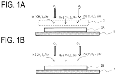
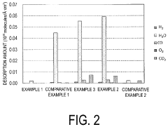
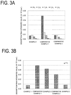
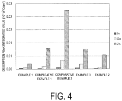
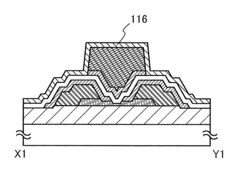
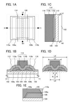
- A semiconductor device with an oxide semiconductor TFT featuring a layered structure including an In-Ga-Zn oxide semiconductor layer with a continuously changing composition intermediate transition layer, formed using the plasma MOCVD method to reduce residual methyl groups and enhance film quality.
Semiconductor device comprising an oxide semiconductor
PatentInactiveUS9812467B2
Innovation
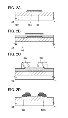
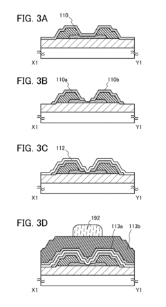
- Incorporating an oxide insulating film and a gate insulating film that supply oxygen to the oxide semiconductor layer, combined with conductive nitride or ruthenium-based metal films for the electrode layers to prevent oxygen diffusion, thereby reducing oxygen vacancies and enhancing electrical stability.
Manufacturing Process Differences
The manufacturing processes for oxide semiconductors and organic semiconductors differ significantly, reflecting their distinct material properties and technological requirements. Oxide semiconductors typically employ vacuum-based deposition techniques such as sputtering, pulsed laser deposition (PLD), and atomic layer deposition (ALD). These methods enable precise control over film thickness and composition, crucial for achieving consistent electronic properties. Sputtering, the most widely used industrial technique for oxide semiconductors, offers excellent scalability and throughput, making it suitable for large-area applications like display backplanes.
In contrast, organic semiconductors utilize solution-based processing methods including spin-coating, inkjet printing, and roll-to-roll printing. These techniques operate at lower temperatures (typically below 200°C) compared to oxide semiconductor processing (300-500°C), reducing energy consumption and enabling compatibility with flexible plastic substrates. The solution processability of organic semiconductors represents a significant manufacturing advantage, potentially lowering production costs through reduced equipment complexity and material usage.
Patterning approaches also differ substantially between these semiconductor types. Oxide semiconductors typically require conventional photolithography and etching processes, involving multiple steps and photoresist materials. Organic semiconductors, however, can be directly patterned through techniques like inkjet printing or screen printing, eliminating several manufacturing steps and reducing waste generation.
The environmental stability during manufacturing presents another key difference. Oxide semiconductor processing generally requires stringent control of oxygen partial pressure and humidity, necessitating sophisticated vacuum systems and environmental controls. Organic semiconductor manufacturing is highly sensitive to solvent purity, ambient conditions, and processing atmosphere, often requiring nitrogen or argon environments to prevent oxidative degradation during deposition and annealing.
Manufacturing yield and defect control strategies also diverge significantly. Oxide semiconductors face challenges related to oxygen vacancy control, interface quality management, and structural uniformity across large areas. Organic semiconductors struggle with molecular orientation control, crystallinity management, and morphological uniformity, particularly in scaled production environments. These different defect mechanisms necessitate distinct in-line monitoring techniques and quality control approaches.
The equipment infrastructure requirements further differentiate these technologies. Oxide semiconductor manufacturing relies on capital-intensive vacuum systems and high-temperature processing equipment similar to those used in conventional silicon manufacturing. Organic semiconductor production can utilize modified versions of existing printing and coating equipment, potentially enabling lower initial capital investment for manufacturing facilities.
Environmental Impact and Sustainability
The environmental impact of semiconductor technologies has become increasingly important as electronic devices proliferate globally. Oxide semiconductors demonstrate significant sustainability advantages over organic semiconductors in several key areas. Their manufacturing processes typically require lower temperatures compared to traditional silicon semiconductors, though still higher than organic alternatives, resulting in moderate energy consumption profiles during production.
Oxide semiconductors exhibit exceptional durability and stability under various environmental conditions, leading to longer device lifespans and reduced electronic waste generation. This longevity represents a substantial sustainability benefit when considering product lifecycle assessments. Additionally, many metal oxide materials used in these semiconductors, such as zinc, indium, and gallium, have established recycling infrastructures, though challenges remain in efficient recovery from complex electronic devices.
In contrast, organic semiconductors offer certain environmental advantages through their potentially lower processing temperatures and compatibility with solution-based manufacturing techniques. These properties can reduce energy requirements during production and enable the use of more environmentally friendly solvents. However, organic semiconductors typically demonstrate shorter operational lifetimes, necessitating more frequent device replacement and potentially generating greater waste volumes over time.
The raw material sourcing presents another important environmental consideration. Oxide semiconductors rely on metal resources that may face supply constraints, particularly for elements like indium. Organic semiconductors, while based on carbon compounds that are theoretically abundant, often require specialized chemical synthesis processes that may involve hazardous precursors or generate significant waste streams.
End-of-life management differs substantially between these technologies. Oxide semiconductor devices can potentially integrate with existing electronic waste recycling systems, though specialized processes may be needed to recover valuable metals efficiently. Organic semiconductor materials present unique challenges for recycling due to their complex polymer structures and potential degradation products.
Water usage patterns also diverge between these technologies. Oxide semiconductor manufacturing typically requires significant water resources for cleaning and processing steps, while some organic semiconductor production methods may be less water-intensive but potentially use more organic solvents that require careful handling and disposal to prevent environmental contamination.
As sustainability becomes a critical factor in technology selection, both semiconductor types are seeing research efforts focused on reducing environmental impacts through greener manufacturing processes, material substitution, and improved recyclability approaches.
Unlock deeper insights with Patsnap Eureka Quick Research — get a full tech report to explore trends and direct your research. Try now!
Generate Your Research Report Instantly with AI Agent
Supercharge your innovation with Patsnap Eureka AI Agent Platform!
