Oxide Semiconductor Patents for TFT and Sensor Applications
SEP 25, 20259 MIN READ
Generate Your Research Report Instantly with AI Agent
Patsnap Eureka helps you evaluate technical feasibility & market potential.
Oxide Semiconductor TFT & Sensor Technology Background
Oxide semiconductors have emerged as a revolutionary material class in the field of thin-film transistors (TFTs) and sensing applications over the past two decades. The journey began with the discovery of transparent conducting oxides (TCOs) in the early 20th century, but significant breakthroughs occurred in 2004 when Hosono's group at Tokyo Institute of Technology demonstrated the first high-performance amorphous oxide semiconductor (AOS) TFTs using indium gallium zinc oxide (IGZO).
The fundamental advantage of oxide semiconductors lies in their unique electronic structure. Unlike conventional amorphous silicon (a-Si), the conduction band in oxide semiconductors is primarily composed of spherically symmetric metal s-orbitals, which overlap significantly even in amorphous states. This characteristic enables high electron mobility (typically 5-50 cm²/Vs) even in amorphous films, overcoming the mobility limitations of a-Si (< 1 cm²/Vs).
The technological evolution of oxide semiconductors has been driven by display industry requirements for higher resolution, lower power consumption, and improved form factors. IGZO TFTs have successfully penetrated commercial markets, appearing in high-end displays from major manufacturers like Sharp, LG, and Samsung since 2012. This commercialization represents one of the fastest transitions from laboratory discovery to mass production in electronic materials history.
Beyond displays, oxide semiconductors have shown remarkable potential in sensor applications due to their unique material properties. Their wide bandgap (typically 3-4 eV) provides excellent optical transparency, while their sensitivity to environmental factors enables various sensing mechanisms. Gas sensors, photodetectors, and biosensors utilizing oxide semiconductors have demonstrated promising performance metrics in research settings.
The patent landscape for oxide semiconductor technology has grown exponentially since 2004, with major technology companies and research institutions securing intellectual property across material compositions, device architectures, and manufacturing processes. Initial patents focused primarily on basic material compositions (IGZO, ZnO, SnO₂), while more recent filings have expanded to novel multi-component systems and specialized device structures for specific applications.
From a geographical perspective, Japan initially dominated oxide semiconductor patent filings, reflecting their pioneering research in this field. However, South Korea, Taiwan, and China have rapidly increased their patent portfolios over the past decade, corresponding with their growing display manufacturing capabilities. The United States and European countries have focused more on specialized applications beyond displays, particularly in sensing and power electronics domains.
Market Analysis for Oxide Semiconductor Applications
The oxide semiconductor market for TFT and sensor applications has experienced substantial growth over the past decade, driven primarily by the expanding display industry and emerging sensor technologies. The global market for oxide semiconductor-based devices reached approximately $15 billion in 2022, with projections indicating a compound annual growth rate (CAGR) of 12.3% through 2028, potentially reaching $30 billion by that time.
The display segment currently dominates the market landscape, accounting for roughly 70% of oxide semiconductor applications. Within this segment, IGZO (Indium Gallium Zinc Oxide) technology has established itself as the preferred material for high-resolution displays in premium smartphones, tablets, and large-format televisions. Major display manufacturers including Samsung, LG Display, and BOE have significantly increased their production capacity for oxide semiconductor-based panels.
Sensor applications represent the fastest-growing segment, with a CAGR exceeding 18%. This growth is fueled by increasing demand for high-performance image sensors, gas sensors, and biosensors across automotive, healthcare, and industrial sectors. The superior electron mobility and stability of oxide semiconductors make them particularly valuable for next-generation sensing technologies requiring high sensitivity and low power consumption.
Regionally, East Asia dominates the market with approximately 65% share, led by manufacturing powerhouses in South Korea, Japan, Taiwan, and China. North America and Europe collectively account for about 25% of the market, primarily focused on R&D and specialized applications. The remaining 10% is distributed across emerging markets, with India and Brazil showing accelerated adoption rates.
Consumer electronics remains the largest end-use sector, representing approximately 55% of market demand. However, industrial applications (18%), automotive (15%), and healthcare (12%) segments are growing rapidly as oxide semiconductor technology finds new applications beyond displays.
Key market drivers include increasing demand for high-resolution, energy-efficient displays, growing adoption of IoT devices requiring advanced sensors, and expanding applications in flexible and transparent electronics. The shift toward OLED and microLED displays incorporating oxide semiconductor backplanes is creating significant market opportunities, while emerging applications in neuromorphic computing and artificial intelligence are opening entirely new market segments.
Technical Challenges in Oxide Semiconductor Development
Despite significant advancements in oxide semiconductor technology for TFT and sensor applications, several technical challenges continue to impede further development and widespread commercial adoption. The most prominent challenge remains the stability and reliability of oxide semiconductor materials under various environmental conditions. Particularly, the sensitivity to oxygen and moisture exposure leads to performance degradation over time, affecting device longevity and consistency in real-world applications.
Carrier mobility limitations present another significant hurdle. While oxide semiconductors offer improved mobility compared to amorphous silicon, they still fall short of crystalline silicon performance. This limitation becomes particularly problematic for high-frequency applications and advanced sensing capabilities where rapid response times are critical. The trade-off between transparency and electrical performance further complicates material optimization efforts.
Interface engineering represents a complex challenge area, as the quality of interfaces between the semiconductor and adjacent layers significantly impacts device performance. Contact resistance issues at metal-semiconductor interfaces often lead to voltage drops and power inefficiencies. Additionally, the formation of stable and defect-free gate dielectric interfaces remains difficult to achieve consistently at scale.
Doping control and uniformity across large-area substrates continue to challenge manufacturers. The precise control of oxygen vacancies, which act as natural dopants in these materials, requires sophisticated deposition techniques and post-processing methods. Variations in doping concentration can lead to threshold voltage shifts and inconsistent device performance across display panels or sensor arrays.
Temperature sensitivity presents another significant barrier, particularly for flexible electronics applications. Many oxide semiconductors exhibit performance variations with temperature fluctuations, limiting their use in environments with wide temperature ranges. This characteristic particularly affects sensor applications where calibration stability is essential.
Manufacturing scalability challenges persist despite years of development. The balance between high-performance material properties and cost-effective, large-scale production techniques remains difficult to achieve. Deposition uniformity across large substrates and the integration of oxide semiconductors with existing manufacturing infrastructure require further optimization.
Emerging applications in transparent and flexible electronics introduce additional challenges related to mechanical durability. Oxide semiconductors often exhibit brittleness that leads to performance degradation under repeated bending or stretching, limiting their application in truly flexible devices. The development of composite materials or novel deposition techniques that maintain electrical properties while enhancing mechanical flexibility represents a critical research direction.
Current Patent Landscape for Oxide Semiconductor TFTs
01 Thin-film transistors using oxide semiconductors
Oxide semiconductors are widely used in thin-film transistors (TFTs) due to their high electron mobility, transparency, and ability to be processed at low temperatures. These materials, particularly indium gallium zinc oxide (IGZO), enable the fabrication of high-performance, transparent electronic devices. The unique properties of oxide semiconductor TFTs make them suitable for applications in displays, sensors, and flexible electronics.- Thin-film transistors using oxide semiconductors: Oxide semiconductors are widely used in thin-film transistor (TFT) applications due to their excellent electrical properties, including high mobility and good stability. These materials enable the fabrication of transparent and flexible electronic devices with improved performance characteristics. The oxide semiconductor layer typically consists of materials such as indium gallium zinc oxide (IGZO) or zinc oxide (ZnO), which can be deposited using various techniques to achieve desired electrical properties.
- Manufacturing methods for oxide semiconductor devices: Various manufacturing techniques are employed to produce high-quality oxide semiconductor devices. These methods include physical vapor deposition (PVD), chemical vapor deposition (CVD), atomic layer deposition (ALD), and solution processing. Post-deposition treatments such as annealing in specific atmospheres are often used to optimize the electrical properties of the oxide semiconductor layer. These manufacturing processes are critical for controlling defects, carrier concentration, and interface quality in the final devices.
- Composition and doping of oxide semiconductors: The composition and doping of oxide semiconductors significantly influence their electrical and optical properties. Common oxide semiconductor materials include zinc oxide (ZnO), indium oxide (In2O3), tin oxide (SnO2), and their various combinations such as indium gallium zinc oxide (IGZO) and indium tin oxide (ITO). Doping these materials with elements like aluminum, gallium, or nitrogen can modify their conductivity, carrier concentration, and band gap, enabling customization for specific applications.
- Applications of oxide semiconductors in electronics: Oxide semiconductors find applications in various electronic devices due to their unique properties. They are used in display technologies (including LCD and OLED displays), transparent electronics, solar cells, gas sensors, and memory devices. Their wide bandgap, optical transparency, and tunable electrical properties make them suitable for both conventional and emerging electronic applications. Recent developments have expanded their use in flexible and wearable electronics.
- Novel structures and architectures using oxide semiconductors: Innovative device structures and architectures leveraging oxide semiconductors have been developed to enhance performance and enable new functionalities. These include multilayer structures, heterojunctions with other semiconductor materials, and three-dimensional device configurations. Such novel architectures can improve carrier transport, reduce leakage current, and enhance stability under various operating conditions. These advancements are pushing the boundaries of what can be achieved with oxide semiconductor technology.
02 Manufacturing processes for oxide semiconductor devices
Various manufacturing techniques are employed to produce oxide semiconductor devices, including sputtering, chemical vapor deposition, and sol-gel methods. These processes can be optimized to control the composition, crystallinity, and defect concentration in the oxide semiconductor layers. Post-deposition treatments such as annealing in different atmospheres can significantly improve the electrical properties and stability of the resulting devices.Expand Specific Solutions03 Novel oxide semiconductor compositions
Research has led to the development of various oxide semiconductor compositions beyond the traditional zinc oxide and indium oxide systems. These include multicomponent oxides containing elements such as gallium, tin, hafnium, and zirconium. The compositional engineering allows for tuning of band gap, carrier concentration, and mobility to meet specific application requirements. These novel materials offer improved stability, performance, and functionality compared to conventional semiconductors.Expand Specific Solutions04 Applications in memory devices and sensors
Oxide semiconductors are increasingly being utilized in memory devices and various sensor applications. Their unique electrical properties make them suitable for resistive random access memory (RRAM), where the resistance state can be switched reversibly. Additionally, the sensitivity of oxide semiconductors to environmental factors such as gases, light, and temperature enables their use in chemical sensors, photodetectors, and temperature sensors with high performance and reliability.Expand Specific Solutions05 Doping and defect engineering in oxide semiconductors
Controlling the electrical properties of oxide semiconductors through doping and defect engineering is crucial for device performance. Intentional introduction of dopants or creation of oxygen vacancies can modify carrier concentration and mobility. Various techniques have been developed to precisely control these parameters, including plasma treatments, ion implantation, and co-deposition with dopant materials. These approaches enable the fabrication of both n-type and p-type oxide semiconductors with tailored properties.Expand Specific Solutions
Key Industry Players in Oxide Semiconductor Field
The oxide semiconductor market for TFT and sensor applications is in a growth phase, with an estimated market size exceeding $5 billion and expanding at a CAGR of 15-20%. The competitive landscape is dominated by Asian companies, particularly Japanese firms like Semiconductor Energy Laboratory and Sharp, alongside Korean giants Samsung Display and LG Display, and Chinese players including BOE Technology and TCL China Star. The technology has reached commercial maturity for display applications, with companies like Sharp and SEL leading in IGZO patent portfolios, while emerging applications in sensors remain in early development stages. Taiwan Semiconductor and Applied Materials provide critical manufacturing technologies, creating a complex ecosystem spanning materials development to device fabrication.
Semiconductor Energy Laboratory Co., Ltd.
Technical Solution: Semiconductor Energy Laboratory (SEL) has pioneered oxide semiconductor technology for TFTs, particularly focusing on IGZO (Indium Gallium Zinc Oxide) materials. Their patented approach involves creating highly stable c-axis aligned crystalline IGZO structures that significantly reduce oxygen vacancies, resulting in improved electron mobility (>10 cm²/Vs) and threshold voltage stability[1]. SEL has developed proprietary deposition techniques that enable precise control of film stoichiometry and crystallinity, allowing for enhanced performance in both display and sensor applications. Their patents cover novel device architectures including dual-gate and back-channel-etch structures that minimize parasitic capacitance and improve switching characteristics[3]. For sensor applications, SEL has developed oxide semiconductor-based photodetectors with high sensitivity across visible and UV spectrums, incorporating unique passivation layers that prevent environmental degradation while maintaining sensitivity[5].
Strengths: Industry-leading expertise in crystalline IGZO technology with superior stability and mobility; extensive patent portfolio covering materials, processes, and device structures. Weaknesses: Higher manufacturing complexity compared to amorphous silicon; requires specialized deposition equipment and processes that may increase production costs.
Samsung Electronics Co., Ltd.
Technical Solution: Samsung Electronics has developed advanced oxide semiconductor technologies for both TFT and sensor applications, with particular emphasis on high-mobility materials for next-generation displays. Their patented approach utilizes unique metal oxide compositions incorporating indium, zinc, and additional dopants like hafnium and titanium to achieve electron mobilities exceeding 30 cm²/Vs while maintaining excellent stability[2]. Samsung's patents cover specialized annealing processes that optimize the microstructure of oxide films, reducing defect states and carrier trapping. For flexible display applications, they've pioneered low-temperature deposition techniques compatible with polymer substrates, enabling bendable and foldable devices[4]. In the sensor domain, Samsung has patented oxide semiconductor-based photodetectors and gas sensors with tailored bandgap engineering to enhance sensitivity to specific wavelengths or target gases. Their multi-layer oxide structures incorporate barrier and passivation technologies that prevent moisture ingress while maintaining electrical performance under mechanical stress[6].
Strengths: Comprehensive vertical integration from materials research to mass production; strong capabilities in flexible oxide semiconductor implementation for foldable displays. Weaknesses: Some patented compositions rely on rare or expensive elements that may impact manufacturing costs; complex multi-layer structures can reduce production yield in high-volume manufacturing.
Critical Patent Analysis for Sensor Applications
Semiconductor device
PatentWO2011055668A1
Innovation
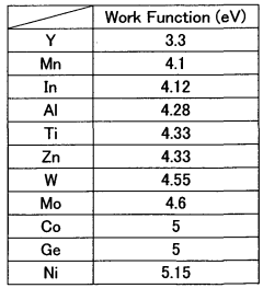
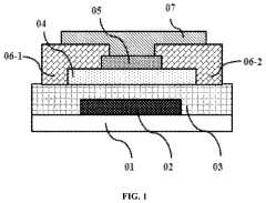
- A stacked-layer structure is employed for the source and drain electrode layers using oxides of metals with lower work functions than the oxide semiconductor layer, such as indium, zinc, or titanium, which form an optimum contact state, allowing for the use of high heat-resistant metals like tungsten or molybdenum, and alloys like indium-zinc or gallium oxynitride, to reduce contact resistance and increase process temperature limits.
Oxide semiconductor thin-film and thin-film transistor consisted thereof
PatentActiveUS11677031B2
Innovation
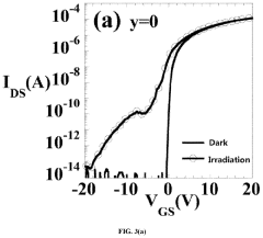
- Doping rare-earth oxides such as praseodymium, terbium, dysprosium, or ytterbium into metal oxide semiconductors to act as light stabilizers, shifting the band structure from direct to indirect gap, reducing photo-induced carriers and maintaining threshold voltage stability under light irradiation without degrading mobility.
Manufacturing Process Optimization Strategies
Manufacturing process optimization for oxide semiconductor TFTs and sensors represents a critical area for technological advancement and cost reduction. Current manufacturing processes face challenges in achieving consistent film quality, precise doping control, and high throughput while maintaining low defect rates. These challenges directly impact device performance, yield rates, and production costs.
The optimization of sputtering parameters has emerged as a primary focus in recent patents. Innovations include multi-target co-sputtering systems that enable precise control of metal ratios in complex oxide compositions such as IGZO (Indium-Gallium-Zinc-Oxide). Advanced process monitoring using in-situ spectroscopic ellipsometry allows real-time adjustment of deposition parameters, significantly improving film uniformity across large substrates.
Low-temperature processing techniques have gained substantial attention, with several patented approaches achieving high-quality oxide semiconductor films at temperatures below 200°C. These innovations enable compatibility with flexible plastic substrates, opening new application domains in wearable sensors and flexible displays. Plasma-enhanced atomic layer deposition (PE-ALD) methods have demonstrated particular promise, offering atomic-level control of film composition and thickness.
Post-deposition treatment strategies represent another significant optimization pathway. Patented techniques include controlled atmosphere annealing processes that effectively reduce oxygen vacancies and improve carrier mobility. Laser annealing methods enable selective crystallization of amorphous oxide films, creating optimized channel regions without subjecting the entire substrate to high temperatures.
Integration of high-k dielectric materials with oxide semiconductors has been addressed through interface engineering patents. These innovations focus on reducing interface trap densities and improving gate dielectric reliability through specialized deposition sequences and surface treatments. Several patents describe multi-layer dielectric structures that minimize leakage current while maintaining high capacitance.
Patterning technologies have evolved to address the specific requirements of oxide semiconductor devices. Self-aligned processes that reduce mask count and improve alignment accuracy have been developed, with several patents describing novel photoresist formulations compatible with oxide semiconductor processing. Dry etching recipes that minimize damage to underlying oxide layers while maintaining pattern fidelity have been optimized for various oxide compositions.
Encapsulation and passivation techniques represent the final critical step in manufacturing optimization. Recent patents describe multilayer barrier structures that effectively prevent moisture ingress while maintaining transparency for display applications. These innovations significantly improve device stability and operational lifetime, particularly for sensors operating in challenging environmental conditions.
IP Strategy and Licensing Considerations
The oxide semiconductor patent landscape presents significant strategic opportunities and challenges for companies operating in the TFT and sensor markets. Establishing a comprehensive IP strategy requires careful consideration of both offensive and defensive approaches. Companies should prioritize building strategic patent portfolios that cover core technologies, manufacturing processes, and novel applications to create competitive barriers and enhance negotiation positions.
Cross-licensing agreements have become increasingly important in the oxide semiconductor field, particularly as the technology matures and finds applications across multiple industries. Organizations with substantial patent portfolios can leverage these assets to gain access to complementary technologies through structured licensing arrangements, reducing litigation risks while expanding technological capabilities. Notable examples include cross-licensing deals between major display manufacturers that have accelerated market adoption while minimizing patent disputes.
Patent pooling represents another strategic approach gaining traction in the oxide semiconductor space. These collaborative arrangements allow multiple patent holders to license their technologies collectively, reducing transaction costs and promoting industry standardization. For emerging applications in flexible electronics and transparent sensors, patent pools could facilitate faster commercialization by providing streamlined access to fundamental IP.
Territorial licensing considerations are particularly relevant for oxide semiconductor technologies, as manufacturing and market dynamics vary significantly across regions. Companies must develop region-specific strategies that account for varying IP enforcement regimes, particularly noting the differences between Asian manufacturing hubs and Western markets. Careful structuring of territorial licenses can maximize revenue while protecting core markets.
Freedom-to-operate (FTO) analysis has become essential before commercializing new oxide semiconductor products. The increasing patent density in this field creates significant infringement risks, necessitating thorough evaluation of existing patent landscapes. Companies should implement systematic FTO processes that identify potential blocking patents early in the development cycle, allowing time for design-around solutions or proactive licensing negotiations.
Value-based licensing models are emerging as alternatives to traditional royalty structures, particularly for sensor applications where the oxide semiconductor technology may represent only a fraction of the final product's value. These models tie compensation to specific performance improvements or cost reductions enabled by the technology, creating more equitable arrangements between licensors and licensees while better reflecting the actual value contribution.
Unlock deeper insights with Patsnap Eureka Quick Research — get a full tech report to explore trends and direct your research. Try now!
Generate Your Research Report Instantly with AI Agent
Supercharge your innovation with Patsnap Eureka AI Agent Platform!