Research on Oxide Semiconductor Electrical Properties and Stability
SEP 25, 202510 MIN READ
Generate Your Research Report Instantly with AI Agent
Patsnap Eureka helps you evaluate technical feasibility & market potential.
Oxide Semiconductor Evolution and Research Objectives
Oxide semiconductors have emerged as a revolutionary material class in the electronics industry over the past several decades. Initially discovered in the 1960s, these materials remained largely academic curiosities until the early 2000s when significant breakthroughs in their processing and performance characteristics catalyzed widespread industrial interest. The evolution of oxide semiconductors has been marked by the transition from traditional silicon-based technologies to more versatile metal oxide compounds, particularly those based on zinc, indium, gallium, and tin.
The fundamental advantage of oxide semiconductors lies in their unique electronic structure, which enables high electron mobility even in amorphous states. This characteristic stands in stark contrast to conventional semiconductors like silicon, which require crystalline structures to achieve comparable performance. The development trajectory has seen progressive improvements in carrier mobility, stability, and uniformity, with each generation addressing specific limitations of its predecessors.
A pivotal moment in oxide semiconductor evolution occurred in 2004 with the introduction of indium-gallium-zinc-oxide (IGZO) by Japanese researchers, demonstrating unprecedented combinations of transparency, processability, and electrical performance. This breakthrough established a new paradigm for thin-film transistor technologies and opened applications previously unattainable with silicon-based semiconductors.
Recent research has increasingly focused on addressing the persistent challenges of electrical stability under environmental stressors such as temperature fluctuations, humidity, and prolonged bias stress. The field has witnessed a shift from empirical optimization toward fundamental understanding of defect physics and charge transport mechanisms at the atomic level, enabling more rational material design approaches.
The primary research objectives in the current landscape center on several critical dimensions. First, enhancing operational stability under diverse environmental conditions remains paramount for commercial viability. Second, developing comprehensive models that accurately predict electrical behavior across different material compositions and processing conditions is essential for accelerating innovation cycles. Third, establishing scalable manufacturing techniques compatible with existing industrial infrastructure represents a key enabler for market penetration.
Additionally, research aims to expand the application spectrum beyond display technologies into emerging fields such as flexible electronics, transparent circuitry, and neuromorphic computing. This expansion necessitates tailoring electrical properties for specific use cases while maintaining fundamental performance advantages. The ultimate goal is to develop oxide semiconductor systems with precisely controllable electrical characteristics, minimal performance variation, and long-term operational reliability across diverse application environments.
Market Analysis for Oxide Semiconductor Applications
The oxide semiconductor market has witnessed substantial growth in recent years, primarily driven by the increasing demand for high-performance display technologies. The global market for oxide semiconductor materials was valued at approximately $3.9 billion in 2022 and is projected to reach $7.2 billion by 2028, representing a compound annual growth rate (CAGR) of 10.7%. This growth trajectory is significantly higher than that of conventional silicon-based semiconductors, which are growing at around 4-5% annually.
The display industry remains the dominant application sector for oxide semiconductors, accounting for nearly 65% of the total market share. Within this segment, thin-film transistor (TFT) backplanes for OLED and LCD displays constitute the largest application area. The superior electrical properties of oxide semiconductors, particularly indium gallium zinc oxide (IGZO), have enabled the development of high-resolution, energy-efficient displays with improved response times.
Consumer electronics manufacturers have been the primary adopters of oxide semiconductor technology, with companies like Samsung, LG, and Apple incorporating these materials into their premium product lines. The smartphone segment alone accounts for approximately 40% of oxide semiconductor applications, followed by tablets (15%), televisions (12%), and monitors (8%).
Emerging application areas showing promising growth include transparent electronics, flexible displays, and power electronics. The transparent electronics market, valued at $1.2 billion in 2022, is expected to grow at a CAGR of 15.3% through 2028, creating new opportunities for oxide semiconductor materials with their unique combination of optical transparency and electrical conductivity.
Regional analysis indicates that East Asia dominates the oxide semiconductor market, with Japan, South Korea, and Taiwan collectively accounting for over 70% of global production capacity. China is rapidly expanding its market presence, with investments in manufacturing facilities increasing by 25% annually over the past three years.
The stability characteristics of oxide semiconductors have opened new market segments in harsh environment applications, including automotive displays, industrial control systems, and medical devices. These sectors value the resistance to temperature fluctuations, humidity, and radiation that oxide semiconductors offer compared to conventional alternatives.
Market challenges include supply chain constraints for critical materials, particularly indium, which has experienced price volatility of up to 30% in recent years. Additionally, competition from emerging technologies such as quantum dot displays and microLED is intensifying, potentially limiting the long-term growth trajectory for certain oxide semiconductor applications.
Current Technical Barriers and Global Development Status
Oxide semiconductor technology faces several critical barriers that impede its widespread commercial adoption. The most significant challenge remains the stability of electrical properties under various environmental conditions. When exposed to prolonged illumination, temperature variations, or bias stress, oxide semiconductors often exhibit threshold voltage shifts and carrier mobility degradation. This instability manifests as performance deterioration in devices over time, particularly affecting display technologies where consistent pixel driving is essential.
Another major technical hurdle involves achieving uniform electrical characteristics across large-area substrates. As display dimensions increase for commercial applications, maintaining homogeneous semiconductor properties becomes exponentially more difficult. Variations in film thickness, composition, and microstructure lead to non-uniform device performance across panels, resulting in visible inconsistencies in consumer products.
Interface engineering represents a persistent challenge, as the semiconductor-dielectric interface quality dramatically influences charge transport and trapping mechanisms. Defects at these interfaces create unwanted states that capture charge carriers, leading to hysteresis effects and unreliable device operation. Despite significant research efforts, creating atomically clean interfaces with minimal defect density remains elusive.
Globally, research on oxide semiconductor electrical properties shows distinct regional focuses. Japan maintains leadership through companies like Sharp and research institutions such as Tokyo Institute of Technology, concentrating on fundamental material science and novel oxide compositions. South Korea dominates industrial implementation through Samsung and LG Display, focusing on manufacturing scalability and integration with existing display technologies.
European research centers, particularly in Germany and the UK, emphasize theoretical modeling of defect physics and band structure engineering. Their contributions have been instrumental in understanding the fundamental mechanisms behind electrical instability. Meanwhile, Chinese institutions have rapidly expanded their research output, particularly in solution-processed oxide semiconductors that promise cost-effective manufacturing routes.
The United States maintains strength in advanced characterization techniques through national laboratories and university collaborations. Recent developments at institutions like Stanford University and MIT have introduced innovative passivation techniques that significantly improve stability under environmental stressors.
Despite these global efforts, the technology readiness level varies significantly across applications. While oxide semiconductors have achieved commercial success in display backplanes, their implementation in logic circuits and power electronics remains at the research stage due to persistent stability and performance limitations. Bridging this gap requires interdisciplinary approaches combining materials science, device physics, and advanced manufacturing techniques.
Existing Methods for Enhancing Electrical Properties
01 Electrical properties of oxide semiconductors
Oxide semiconductors exhibit unique electrical properties that make them suitable for various electronic applications. These materials can be engineered to have specific conductivity, carrier mobility, and band gap characteristics. The electrical properties can be tuned by controlling the composition, crystal structure, and defect concentration in the oxide semiconductor. These materials often show a good balance between transparency and conductivity, making them valuable for transparent electronics.- Electrical properties of oxide semiconductors: Oxide semiconductors exhibit unique electrical properties that make them suitable for various electronic applications. These materials can be engineered to have specific conductivity, carrier mobility, and band gap characteristics. The electrical properties can be tuned by controlling the composition, crystal structure, and processing conditions. Factors such as oxygen vacancy concentration and dopant incorporation significantly influence the electrical behavior of these materials.
- Stability enhancement techniques for oxide semiconductors: Various methods can be employed to enhance the stability of oxide semiconductor materials. These include thermal annealing processes, surface passivation techniques, and incorporation of stabilizing additives. Environmental factors such as humidity, temperature, and light exposure can affect the long-term stability of these materials. Proper encapsulation and protective layers can significantly improve the operational lifetime and reliability of oxide semiconductor devices.
- Doping strategies to modify oxide semiconductor properties: Doping is a critical approach to modify the electrical properties and stability of oxide semiconductors. Introduction of specific elements can control carrier concentration, improve conductivity, and enhance environmental stability. Different dopants can be used to create n-type or p-type semiconductors, allowing for the fabrication of various electronic components. The concentration and distribution of dopants significantly impact the performance and reliability of oxide semiconductor devices.
- Thin film deposition techniques for oxide semiconductors: Various deposition methods are employed to create high-quality oxide semiconductor thin films with controlled properties. These include physical vapor deposition, chemical vapor deposition, atomic layer deposition, and solution-based processes. The deposition parameters significantly influence the microstructure, composition, and electrical characteristics of the resulting films. Post-deposition treatments such as annealing in specific atmospheres can further optimize the electrical properties and stability of these materials.
- Interface engineering for improved device performance: The interfaces between oxide semiconductors and other materials in electronic devices play a crucial role in determining overall performance and stability. Interface engineering techniques include the use of buffer layers, surface treatments, and controlled growth processes to minimize defects and charge trapping. Proper interface design can reduce contact resistance, improve carrier transport, and enhance long-term operational stability. This is particularly important in transistors, sensors, and optoelectronic devices based on oxide semiconductors.
02 Stability enhancement techniques for oxide semiconductors
Various methods can be employed to enhance the stability of oxide semiconductors, particularly under environmental stresses such as temperature, humidity, and electrical bias. These techniques include passivation layers, annealing processes, and compositional modifications. Introducing specific dopants or creating multi-component oxide systems can significantly improve the long-term stability of these materials. Surface treatments and encapsulation methods are also effective in protecting oxide semiconductors from degradation.Expand Specific Solutions03 Thin-film transistor applications of oxide semiconductors
Oxide semiconductors are widely used in thin-film transistors (TFTs) due to their favorable electrical properties and processing compatibility. These TFTs exhibit good field-effect mobility, low threshold voltage, and excellent on/off current ratios. The stability of oxide semiconductor TFTs under bias stress and environmental conditions is critical for their application in display technologies. Various oxide compositions and device architectures have been developed to optimize TFT performance and reliability.Expand Specific Solutions04 Defect engineering and doping strategies
Controlling defects and implementing effective doping strategies are essential for optimizing the electrical properties and stability of oxide semiconductors. Oxygen vacancies, metal interstitials, and grain boundaries significantly influence carrier concentration and mobility. Intentional doping with specific elements can enhance conductivity, modify the band structure, and improve stability. Post-deposition treatments such as annealing in controlled atmospheres can be used to manipulate defect concentrations and distribution.Expand Specific Solutions05 Deposition methods and process optimization
Various deposition techniques can be used to fabricate oxide semiconductor films with controlled properties and enhanced stability. These methods include sputtering, chemical vapor deposition, atomic layer deposition, and solution processing. The deposition parameters significantly affect the microstructure, composition, and interface quality of the oxide semiconductor films. Optimizing these processes is crucial for achieving reproducible electrical properties and long-term stability in devices based on oxide semiconductors.Expand Specific Solutions
Leading Research Institutions and Industrial Manufacturers
The oxide semiconductor technology landscape is currently in a growth phase, with increasing market adoption driven by superior electrical properties and stability advantages. The market is expanding rapidly, particularly in display technologies, power electronics, and memory applications, with an estimated global market size exceeding $3 billion. From a technical maturity perspective, companies like Samsung Electronics, Taiwan Semiconductor Manufacturing Co., and Sharp Corp. are leading commercial deployment, while specialized players such as Semiconductor Energy Laboratory and FLOSFIA are advancing fundamental research in novel oxide materials. Japan Display and LG Chem are focusing on display applications, while academic institutions including Kyoto University and South China University of Technology are contributing to fundamental understanding of stability mechanisms. The technology is transitioning from early commercialization to mainstream adoption across multiple semiconductor applications.
Semiconductor Energy Laboratory Co., Ltd.
Technical Solution: Semiconductor Energy Laboratory (SEL) has pioneered advanced oxide semiconductor technology, particularly focusing on IGZO (Indium Gallium Zinc Oxide) thin-film transistors. Their research has demonstrated remarkable electrical properties with electron mobility exceeding 10 cm²/Vs while maintaining extremely low off-state current (below 10^-13 A). SEL has developed proprietary crystallization techniques that enhance the stability of oxide semiconductors through controlled annealing processes and passivation layers that effectively suppress oxygen vacancy formation. Their c-axis aligned crystalline oxide semiconductor technology (CAAC-OS) exhibits exceptional stability against environmental stressors including light, heat, and electrical stress. SEL has also implemented hydrogen and nitrogen doping methods to control carrier concentration and improve threshold voltage stability, resulting in devices that maintain consistent performance characteristics over extended operational periods.
Strengths: Industry-leading expertise in crystalline oxide semiconductors with superior stability against environmental factors; proprietary CAAC-OS technology offers exceptional reliability for display applications. Weaknesses: Manufacturing processes may require higher temperatures than amorphous alternatives, potentially limiting substrate compatibility and increasing production costs.
Samsung Electronics Co., Ltd.
Technical Solution: Samsung has developed advanced oxide semiconductor technology focusing on indium-zinc-oxide (IZO) and indium-gallium-zinc-oxide (IGZO) materials for display applications. Their research has yielded high-performance oxide TFTs with field-effect mobility exceeding 20 cm²/Vs while maintaining excellent uniformity across large substrates. Samsung's approach involves precise control of oxygen partial pressure during deposition and post-deposition annealing to optimize electrical properties. They've implemented multi-layer oxide semiconductor structures with carefully engineered interfaces to enhance stability against bias stress and illumination. Their proprietary passivation techniques using silicon nitride and aluminum oxide layers effectively suppress ambient degradation mechanisms. Samsung has also pioneered the integration of oxide semiconductors with flexible substrates, developing specialized low-temperature processes that maintain electrical performance while enabling bendable displays. Their research includes compensation circuit designs that mitigate threshold voltage shifts over time, ensuring consistent display performance throughout device lifetime.
Strengths: Exceptional manufacturing capability for large-area oxide semiconductor implementation; strong integration with display technology ecosystem; advanced compensation techniques for long-term stability. Weaknesses: Proprietary nature of technology may limit broader industry adoption; some approaches may prioritize performance over cost-effectiveness for certain applications.
Critical Patents and Breakthroughs in Stability Enhancement
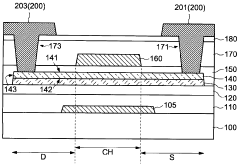
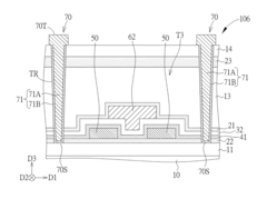
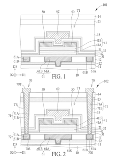
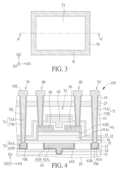
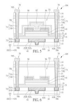
Semiconductor device
PatentWO2023228616A1
Innovation
- A semiconductor device configuration featuring a metal oxide layer containing aluminum, an oxide semiconductor layer with distinct crystal regions, and a gas barrier function to reduce oxygen vacancies and defects, including a dual-gate transistor structure with a metal oxide layer covering the oxide semiconductor layer to enhance oxygen supply and reduce interface state density.
Oxide semiconductor device
PatentInactiveUS20180033891A1
Innovation
- A protection wall is implemented around the oxide semiconductor transistor, extending vertically and laterally to block environmental substances, enhancing the protective abilities and preventing their entry into the oxide semiconductor layer.
Material Characterization Techniques and Standards
The characterization of oxide semiconductor materials requires sophisticated analytical techniques to accurately assess their electrical properties and stability. X-ray diffraction (XRD) stands as a fundamental method for determining crystal structure, phase composition, and lattice parameters, providing essential insights into material quality and structural defects that influence electrical performance. Complementary to XRD, X-ray photoelectron spectroscopy (XPS) enables precise analysis of chemical states and composition at surfaces and interfaces, critical for understanding charge transport mechanisms.
High-resolution transmission electron microscopy (HRTEM) offers nanoscale visualization of crystal structures and defects, while scanning electron microscopy (SEM) provides morphological information at the microscale. These imaging techniques, when combined with energy-dispersive X-ray spectroscopy (EDX), deliver comprehensive elemental mapping crucial for identifying compositional variations that affect device performance.
For direct electrical characterization, Hall effect measurements remain the gold standard for determining carrier concentration, mobility, and carrier type. Temperature-dependent Hall measurements further reveal activation energies and transport mechanisms. Four-point probe techniques enable accurate resistivity measurements while eliminating contact resistance effects, particularly valuable for thin-film oxide semiconductors.
Standardization of these characterization methods is essential for reliable comparison across research groups and industrial applications. The International Organization for Standardization (ISO) and American Society for Testing and Materials (ASTM) have established protocols for semiconductor material characterization, though specific standards for oxide semiconductors continue to evolve. These standards address sample preparation, measurement conditions, and data analysis methodologies to ensure reproducibility.
Bias-temperature stress testing represents a critical stability assessment technique, subjecting devices to elevated temperatures under electrical bias to accelerate degradation mechanisms. Standardized protocols typically specify stress conditions (voltage, temperature, duration) and measurement intervals to quantify threshold voltage shifts and mobility changes over time.
Advanced techniques including deep-level transient spectroscopy (DLTS) and admittance spectroscopy provide detailed information about trap states and defect energy levels that significantly impact device stability. These methods are increasingly standardized for oxide semiconductor evaluation, with measurement parameters optimized for the unique characteristics of these materials.
Emerging characterization approaches such as operando measurements, which monitor material properties during device operation, are gaining prominence but lack comprehensive standardization. The development of unified protocols for these advanced techniques represents a significant opportunity for improving oxide semiconductor research and development efficiency.
Environmental Impact and Sustainability Considerations
The environmental impact of oxide semiconductor technology represents a critical consideration in the broader context of sustainable electronics development. Oxide semiconductors offer significant advantages over conventional silicon-based technologies in terms of reduced material consumption and energy requirements during manufacturing. The thin-film deposition processes typically used for oxide semiconductors, such as sputtering and atomic layer deposition, generally require lower temperatures than silicon processing, resulting in reduced energy consumption and associated carbon emissions.
Material composition presents both challenges and opportunities for environmental sustainability. While many oxide semiconductors utilize abundant elements like zinc, tin, and indium, concerns exist regarding the limited global supply of indium, which is essential for indium gallium zinc oxide (IGZO) formulations. This has prompted research into alternative compositions using more earth-abundant elements, such as zinc tin oxide (ZTO) systems, which maintain similar electrical properties while reducing dependence on scarce resources.
The operational efficiency of oxide semiconductor devices contributes positively to environmental sustainability. Their low power consumption, particularly in display applications, translates to reduced energy requirements throughout product lifecycles. This characteristic becomes increasingly important as electronic devices proliferate globally, with potential energy savings at scale representing significant environmental benefits.
End-of-life considerations for oxide semiconductor technologies reveal promising attributes. The relatively simple material compositions of many oxide semiconductors potentially facilitate recycling processes compared to more complex semiconductor structures. However, integration challenges remain when these materials are incorporated into complex electronic systems with numerous other components and materials.
Toxicity profiles of oxide semiconductors generally compare favorably to alternatives containing lead, arsenic, or other highly toxic elements. Nevertheless, comprehensive lifecycle assessments are necessary to fully understand environmental impacts from raw material extraction through manufacturing, use, and disposal phases. Recent research indicates that optimizing stability mechanisms in oxide semiconductors can extend device lifetimes, thereby reducing electronic waste generation.
Regulatory frameworks increasingly influence development trajectories in this field. The European Union's Restriction of Hazardous Substances (RoHS) and Registration, Evaluation, Authorization and Restriction of Chemicals (REACH) regulations have accelerated research into environmentally benign semiconductor materials and processing methods. These regulatory pressures, combined with corporate sustainability initiatives, are driving innovation toward greener oxide semiconductor technologies with reduced environmental footprints.
Unlock deeper insights with Patsnap Eureka Quick Research — get a full tech report to explore trends and direct your research. Try now!
Generate Your Research Report Instantly with AI Agent
Supercharge your innovation with Patsnap Eureka AI Agent Platform!