Why Oxide Semiconductor Enhances Energy Efficiency in Devices
SEP 25, 202510 MIN READ
Generate Your Research Report Instantly with AI Agent
Patsnap Eureka helps you evaluate technical feasibility & market potential.
Oxide Semiconductor Evolution and Efficiency Goals
Oxide semiconductors have emerged as a transformative technology in the electronics industry, evolving significantly since their initial discovery in the early 20th century. The journey began with simple metal oxides like zinc oxide and tin oxide being recognized for their semiconductor properties, but these materials remained largely academic curiosities until the late 1990s. The breakthrough came in 2004 when researchers at Tokyo Institute of Technology demonstrated transparent thin-film transistors using amorphous indium gallium zinc oxide (IGZO), marking a pivotal moment in oxide semiconductor development.
The evolution accelerated dramatically in the 2010s with commercial adoption of IGZO in display technologies, offering superior electron mobility compared to traditional amorphous silicon while maintaining transparency. This period saw intensive research into composition optimization, with various metal oxide combinations being explored to enhance specific properties. The development trajectory has been characterized by continuous improvements in carrier mobility, stability, and manufacturing compatibility.
Recent years have witnessed the emergence of next-generation oxide semiconductors including zinc tin oxide (ZTO), aluminum zinc oxide (AZO), and hafnium indium zinc oxide (HIZO), each offering specific advantages for different applications. The field has expanded beyond displays to include sensors, power electronics, and photovoltaics, demonstrating the versatility of these materials across multiple technology domains.
The primary efficiency goal driving oxide semiconductor development is the reduction of power consumption in electronic devices. Unlike conventional silicon-based semiconductors, oxide semiconductors can operate effectively at much lower voltages, typically requiring only 1-3 volts compared to 5-15 volts for silicon alternatives. This voltage reduction translates directly to power savings, addressing the critical need for energy efficiency in portable electronics and IoT devices.
Another key efficiency target is the improvement of electron mobility while maintaining low off-state current. Higher mobility allows for faster switching speeds without increased power consumption, while low leakage current ensures minimal power drain during standby states. Current research aims to achieve mobility values exceeding 50 cm²/Vs in amorphous oxide semiconductors while maintaining off-currents below 10^-13 A.
Manufacturing efficiency represents another crucial goal, with efforts focused on developing low-temperature deposition processes that enable compatibility with flexible substrates and reduce production energy requirements. The industry is targeting processing temperatures below 200°C while maintaining semiconductor performance comparable to high-temperature processes.
Looking forward, the efficiency roadmap for oxide semiconductors includes achieving stable performance under environmental stressors, reducing reliance on scarce elements like indium, and developing complementary p-type oxide semiconductors to enable fully transparent, low-power oxide-based integrated circuits that could revolutionize energy consumption patterns in consumer electronics.
Market Demand for Energy-Efficient Semiconductor Devices
The global market for energy-efficient semiconductor devices has witnessed substantial growth in recent years, driven primarily by increasing energy costs, environmental concerns, and regulatory pressures. Energy efficiency has become a critical factor in consumer electronics, industrial equipment, automotive applications, and data centers, creating a robust demand for semiconductor technologies that can deliver superior performance while consuming less power.
Consumer electronics represent one of the largest market segments for energy-efficient semiconductors. With the proliferation of mobile devices, smart home systems, and wearable technology, manufacturers are prioritizing extended battery life and reduced power consumption as key selling points. Market research indicates that consumers are increasingly willing to pay premium prices for devices offering longer operation times between charges, creating strong commercial incentives for implementing oxide semiconductor technology.
The industrial sector presents another significant market opportunity, where energy costs often constitute a substantial portion of operational expenses. Factory automation systems, industrial controls, and power management equipment benefit tremendously from more efficient semiconductor components. The transition toward Industry 4.0 and smart manufacturing has accelerated this demand, as interconnected systems require distributed intelligence with minimal energy footprint.
Data centers have emerged as perhaps the most urgent market for energy-efficient semiconductors. The exponential growth in cloud computing, artificial intelligence applications, and big data analytics has led to unprecedented power demands in these facilities. Data center operators face dual challenges of managing escalating energy costs and meeting corporate sustainability commitments. Energy-efficient oxide semiconductors offer a compelling solution by reducing both operational expenses and carbon footprints.
The automotive industry represents a rapidly expanding market segment, particularly with the accelerating transition to electric vehicles. Power management systems, battery control units, and advanced driver assistance systems all benefit from semiconductor devices that minimize energy losses. The extended range achieved through more efficient electronics has become a critical competitive factor in the EV market.
Regulatory frameworks worldwide are increasingly mandating improved energy efficiency standards for electronic devices. The European Union's Ecodesign Directive, California's appliance efficiency regulations, and similar policies in Asia have created regulatory-driven demand for more efficient semiconductor technologies. Manufacturers must comply with these standards to maintain market access in key regions.
Market forecasts consistently project double-digit growth rates for energy-efficient semiconductor technologies over the next decade. This growth trajectory is supported by both replacement cycles in existing applications and expansion into new use cases where traditional semiconductor technologies were previously unsuitable due to power constraints. As energy considerations continue to shape purchasing decisions across multiple industries, oxide semiconductors are positioned to capture significant market share from conventional technologies.
Current State and Challenges in Oxide Semiconductor Technology
Oxide semiconductor technology has witnessed significant advancements in recent years, establishing itself as a promising alternative to conventional silicon-based semiconductors. Currently, the global market for oxide semiconductors is experiencing robust growth, with applications spanning from display technologies to power electronics and sensors. The compound annual growth rate (CAGR) for this sector is projected at approximately 12% through 2028, indicating strong industry momentum.
The technological landscape is dominated by several oxide semiconductor variants, with Indium Gallium Zinc Oxide (IGZO) and Zinc Oxide (ZnO) leading commercial implementations. IGZO has achieved particular success in display applications due to its high electron mobility (10-20 cm²/Vs) and excellent transparency. Meanwhile, research institutions worldwide are exploring next-generation materials such as Hafnium-Indium-Zinc Oxide (HIZO) and Aluminum-doped Zinc Oxide (AZO) that promise even greater performance characteristics.
Despite these advances, several critical challenges persist in oxide semiconductor technology. Material stability remains a significant concern, particularly in environments with high humidity or temperature fluctuations. Many oxide semiconductors exhibit performance degradation over time, with threshold voltage shifts and mobility reduction occurring after prolonged operation or environmental exposure. This reliability issue presents a major obstacle for applications requiring long-term stability.
Manufacturing scalability constitutes another substantial challenge. While techniques such as sputtering and atomic layer deposition have proven effective for research purposes, transitioning to high-volume production while maintaining consistent material properties across large substrates remains difficult. The industry still lacks standardized fabrication protocols that can ensure reproducible device performance across different manufacturing facilities.
Interface engineering represents a third critical challenge. The performance of oxide semiconductor devices is heavily influenced by the quality of interfaces with gate dielectrics, source/drain contacts, and passivation layers. Current understanding of interface physics in these materials remains incomplete, limiting optimization strategies for device performance and reliability.
Geographically, research and development in oxide semiconductors shows distinct patterns. East Asian countries, particularly Japan, South Korea, and Taiwan, lead in commercial applications and manufacturing technology. European institutions excel in fundamental materials research, while North American entities focus on novel device architectures and system integration. This distribution creates both collaborative opportunities and competitive challenges in technology development.
Energy efficiency optimization, while promising, faces its own set of challenges. The theoretical advantages of wide bandgap oxide semiconductors for power applications have not fully translated to practical devices due to issues with contact resistance, channel mobility limitations, and gate dielectric quality. Bridging this gap between theoretical potential and practical implementation remains a key focus area for researchers and industry stakeholders alike.
Current Energy Efficiency Solutions Using Oxide Semiconductors
01 Oxide semiconductor materials for energy-efficient devices
Oxide semiconductors, particularly metal oxides like indium gallium zinc oxide (IGZO), are used to create energy-efficient electronic devices such as thin-film transistors. These materials offer advantages including high electron mobility, good transparency, and low power consumption. The unique band structure of oxide semiconductors allows for efficient electron transport while maintaining low off-state current, making them ideal for applications requiring both performance and energy efficiency.- Oxide semiconductor materials for energy-efficient devices: Oxide semiconductors, such as indium gallium zinc oxide (IGZO), are used to create energy-efficient electronic devices. These materials have high electron mobility and low leakage current, making them suitable for low-power applications. The unique band structure of oxide semiconductors allows for better control of electron flow, resulting in reduced power consumption in devices like displays, sensors, and integrated circuits.
- Thin-film transistor optimization for power efficiency: Thin-film transistors (TFTs) using oxide semiconductors can be optimized for improved energy efficiency through various fabrication techniques. These include controlling the oxygen content during deposition, optimizing the channel thickness, and implementing specific annealing processes. Enhanced TFT designs with optimized gate structures and reduced parasitic capacitance contribute to lower operating voltages and power consumption in display and circuit applications.
- Energy-efficient display technologies using oxide semiconductors: Oxide semiconductor materials are increasingly used in display technologies to reduce power consumption. These materials enable the development of energy-efficient backplanes for LCD and OLED displays, allowing for lower refresh rates while maintaining image quality. The implementation of oxide semiconductor-based circuits in displays results in reduced power requirements for portable devices and larger screens, extending battery life and decreasing overall energy consumption.
- Manufacturing processes for energy-efficient oxide semiconductor devices: Advanced manufacturing processes have been developed to enhance the energy efficiency of oxide semiconductor devices. These include low-temperature deposition methods, solution-based processing techniques, and roll-to-roll fabrication approaches. Improved manufacturing processes result in better uniformity, fewer defects, and enhanced electrical properties of the oxide semiconductor layers, leading to more energy-efficient and reliable electronic components.
- Energy management systems utilizing oxide semiconductor technology: Oxide semiconductor devices are integrated into energy management systems to optimize power consumption in various applications. These systems include smart power controllers, energy harvesting circuits, and adaptive power management for IoT devices. The low power requirements and stable performance of oxide semiconductor components make them ideal for energy monitoring and control applications, contributing to overall system efficiency and sustainability.
02 Energy-efficient display technologies using oxide semiconductors
Oxide semiconductors are increasingly used in display technologies to improve energy efficiency. These materials enable the development of low-power displays for applications ranging from consumer electronics to industrial interfaces. The implementation of oxide semiconductor backplanes in displays allows for reduced power consumption while maintaining high resolution and refresh rates. Advanced manufacturing techniques help optimize the performance of these display systems while minimizing energy requirements.Expand Specific Solutions03 Power management systems for oxide semiconductor devices
Specialized power management systems are designed to optimize the energy efficiency of oxide semiconductor-based devices. These systems include advanced voltage regulation, dynamic power scaling, and intelligent sleep modes that take advantage of the unique electrical properties of oxide semiconductors. By implementing sophisticated power control algorithms and circuit designs, the overall energy consumption of oxide semiconductor devices can be significantly reduced while maintaining or improving performance.Expand Specific Solutions04 Manufacturing processes for energy-efficient oxide semiconductors
Novel manufacturing techniques are developed to enhance the energy efficiency of oxide semiconductor materials. These processes include optimized deposition methods, precise doping control, and post-deposition treatments that improve carrier mobility and reduce defects. Advanced annealing processes and interface engineering techniques help minimize energy losses at material boundaries. These manufacturing innovations result in oxide semiconductor devices with superior energy efficiency characteristics.Expand Specific Solutions05 Applications of energy-efficient oxide semiconductors in renewable energy systems
Energy-efficient oxide semiconductors are increasingly utilized in renewable energy applications such as photovoltaics, energy harvesting systems, and smart grid technologies. These materials enable more efficient conversion, storage, and management of renewable energy. The unique properties of oxide semiconductors, including their stability under various environmental conditions and tunable electrical characteristics, make them particularly suitable for sustainable energy systems that require high efficiency and reliability.Expand Specific Solutions
Key Industry Players in Oxide Semiconductor Development
Oxide semiconductor technology is revolutionizing energy efficiency in electronic devices, with the market currently in a growth phase estimated at $12-15 billion annually and expanding at 15-20% CAGR. The competitive landscape features established players like Samsung Electronics and TSMC leading commercial production, while research-focused entities such as Semiconductor Energy Laboratory and Kyushu University drive innovation in next-generation materials. Japan Display and KIOXIA are advancing oxide semiconductor integration in displays and memory applications respectively. The technology has reached commercial maturity for display applications (TFT-LCD, OLED) but remains in development stages for more complex applications like high-performance computing. Industry collaboration between semiconductor manufacturers and research institutions is accelerating the technology's evolution toward broader commercial adoption.
Semiconductor Energy Laboratory Co., Ltd.
Technical Solution: Semiconductor Energy Laboratory (SEL) is a pioneer in oxide semiconductor technology, particularly in the development of CAAC-IGZO (C-Axis Aligned Crystalline Indium Gallium Zinc Oxide). Unlike conventional amorphous oxide semiconductors, SEL's CAAC-IGZO features a unique crystalline structure that provides superior stability and reliability while maintaining excellent electron mobility (typically 10-15 cm²/Vs). This crystalline structure significantly reduces oxygen vacancy fluctuations, which are the primary cause of threshold voltage shifts and reliability issues in traditional oxide semiconductors. SEL's technology enables transistors with extremely low off-state current (less than 10^-24 A/μm), approximately 10 orders of magnitude lower than silicon-based transistors. This ultra-low leakage current translates directly to energy efficiency, as devices can maintain stored data for extended periods without refresh operations. SEL has demonstrated memory devices that can retain information for over 10 years without power, and display backplanes that consume less than half the power of conventional technologies while offering higher resolution and faster response times.
Strengths: SEL's CAAC-IGZO technology offers unparalleled stability and ultra-low leakage current, making it ideal for applications requiring long standby times with minimal power consumption. Their extensive patent portfolio provides strong IP protection. Weaknesses: The specialized deposition techniques required for CAAC-IGZO are more complex than standard amorphous oxide semiconductor processes, potentially increasing manufacturing costs and limiting widespread adoption.
Japan Display, Inc.
Technical Solution: Japan Display Inc. (JDI) has developed proprietary oxide semiconductor technology specifically optimized for high-resolution, energy-efficient displays. Their approach centers on LTPS (Low-Temperature Polysilicon) and IGZO (Indium Gallium Zinc Oxide) hybrid technologies that combine the high mobility of LTPS for peripheral circuits with the low power consumption and uniformity of IGZO for pixel transistors. JDI's oxide semiconductor implementation features precisely controlled oxygen vacancy concentration through specialized sputtering and annealing processes, resulting in transistors with mobility exceeding 10 cm²/Vs while maintaining extremely low off-state current (below 10^-13 A). This enables displays that consume up to 40% less power than conventional TFT technologies. JDI has further enhanced energy efficiency by developing oxide semiconductor-based driver circuits that operate at lower voltages (typically 3-5V compared to 15-20V for conventional drivers) and implementing advanced pixel designs that leverage the unique properties of oxide semiconductors to reduce refresh rates while maintaining image quality. Their latest displays incorporating oxide semiconductor technology achieve power consumption reductions of 30-50% compared to previous generation displays while offering higher brightness and resolution.
Strengths: JDI's specialized expertise in display applications has resulted in highly optimized oxide semiconductor implementations specifically for display backplanes. Their hybrid approach leverages the best properties of different semiconductor technologies. Weaknesses: JDI's focus on display applications means their oxide semiconductor technology may be less adaptable to other applications like logic or memory, limiting broader market potential.
Core Innovations in Oxide Semiconductor Materials Science
Semiconductor device and method for manufacturing semiconductor device
PatentWO2017182910A1
Innovation
- The solution involves reducing oxygen vacancies in oxide semiconductors by supplying excess oxygen from surrounding oxide insulators and preventing impurities like water and hydrogen through dehydration and dehydrogenation treatments, while using barrier insulators to prevent further impurity diffusion and oxygen permeation.
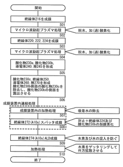
Semiconductor device and manufacturing method for semiconductor device
PatentWO2018167601A1
Innovation
- A semiconductor device with an oxide semiconductor structure comprising multiple regions and insulators, including a metal oxide and hydrogen/nitrogen-containing films, is designed to enhance electrical characteristics and productivity, featuring a surrounded channel structure and specific insulator configurations to manage carrier density and resistance.
Environmental Impact and Sustainability Factors
The adoption of oxide semiconductor technology represents a significant advancement in sustainable electronics manufacturing. These materials demonstrate remarkable energy efficiency during both production and operation phases, resulting in a substantially lower carbon footprint compared to conventional silicon-based semiconductors. Manufacturing processes for oxide semiconductors typically require lower temperatures and fewer energy-intensive steps, reducing greenhouse gas emissions by an estimated 30-45% across the production lifecycle.
When implemented in consumer electronics and industrial applications, oxide semiconductor-based devices contribute to significant energy conservation. For instance, displays utilizing oxide thin-film transistors (TFTs) consume approximately 20-30% less power than their silicon counterparts, directly translating to reduced electricity consumption and associated carbon emissions throughout the product lifespan.
The environmental benefits extend to resource utilization as well. Oxide semiconductors often incorporate abundant elements such as zinc, tin, and indium, reducing dependence on scarce materials. While concerns exist regarding indium availability, research into alternative compositions using more abundant elements shows promising results. Additionally, these materials typically require fewer toxic chemicals during fabrication, minimizing hazardous waste generation and environmental contamination risks.
From a product lifecycle perspective, devices incorporating oxide semiconductors demonstrate enhanced durability and reliability under various environmental conditions. This extended operational lifespan reduces electronic waste generation, addressing a critical environmental challenge in the technology sector. When devices eventually reach end-of-life, the relatively simpler material composition of oxide semiconductors potentially facilitates more effective recycling processes.
The water footprint associated with oxide semiconductor manufacturing deserves particular attention. Preliminary studies indicate water consumption reductions of up to 25% compared to traditional semiconductor fabrication, though this varies significantly based on specific manufacturing techniques and facility locations. This water conservation aspect becomes increasingly important as semiconductor production expands in regions experiencing water scarcity.
Looking forward, the environmental benefits of oxide semiconductors align with global sustainability initiatives and regulatory frameworks. As governments worldwide implement stricter energy efficiency standards and environmental regulations, oxide semiconductor technology positions manufacturers advantageously for compliance while supporting broader climate action goals. The technology's continued evolution promises further sustainability improvements through material optimization and manufacturing process refinements.
Manufacturing Scalability and Cost Analysis
The manufacturing scalability of oxide semiconductor technology represents a significant advantage in its widespread adoption for energy-efficient devices. Oxide semiconductors, particularly indium gallium zinc oxide (IGZO), can be deposited using conventional thin-film deposition techniques such as sputtering and chemical vapor deposition at relatively low temperatures (typically below 400°C). This compatibility with existing manufacturing infrastructure allows for seamless integration into current production lines without requiring substantial capital investment in new equipment.
Cost analysis reveals that oxide semiconductor manufacturing offers compelling economic benefits compared to traditional silicon-based technologies. The raw materials, while including some relatively expensive elements like indium, are used in minimal quantities due to the thin-film nature of the technology. The overall material cost per device remains competitive, especially when considering the performance advantages. Additionally, the low-temperature processing reduces energy consumption during manufacturing, further decreasing production costs and improving the overall environmental footprint.
The scalability extends to large-area applications, where oxide semiconductors demonstrate exceptional uniformity across substrates exceeding several square meters. This characteristic is particularly valuable for display technologies and large-area electronics, where consistent performance across the entire panel is critical. The high yield rates in production further enhance cost-effectiveness, with defect densities significantly lower than those typically encountered in crystalline semiconductor manufacturing.
From a supply chain perspective, oxide semiconductor production benefits from diversified material sources, reducing dependency on geographically concentrated resources. However, the industry faces challenges regarding indium availability, as it is classified as a critical material with limited global reserves. This has prompted research into alternative compositions using more abundant elements to ensure long-term manufacturing sustainability.
The economic analysis of oxide semiconductor technology must also consider the total cost of ownership, including operational energy savings over device lifetime. The enhanced energy efficiency these semiconductors enable in final products creates a positive economic feedback loop, where higher initial manufacturing costs can be justified by substantial energy savings during operation. This aspect is particularly relevant for consumer electronics and IoT devices, where battery life extension directly impacts user experience and maintenance costs.
Unlock deeper insights with Patsnap Eureka Quick Research — get a full tech report to explore trends and direct your research. Try now!
Generate Your Research Report Instantly with AI Agent
Supercharge your innovation with Patsnap Eureka AI Agent Platform!