Comparison of Oxide Semiconductor vs Silicon-Based Devices
SEP 25, 20259 MIN READ
Generate Your Research Report Instantly with AI Agent
Patsnap Eureka helps you evaluate technical feasibility & market potential.
Oxide vs Silicon Semiconductor Evolution and Objectives
The evolution of semiconductor technology has been a cornerstone of modern electronics, with silicon dominating the industry for decades. Silicon-based semiconductors emerged in the 1950s, revolutionizing electronics with the invention of the transistor and integrated circuit. These developments established silicon as the primary material for semiconductor manufacturing due to its abundance, stability, and suitable electronic properties. The industry has followed Moore's Law, doubling transistor density approximately every two years, driving continuous miniaturization and performance improvements.
Oxide semiconductors represent a significant divergence from this established path. First gaining prominence in the early 2000s with materials like indium gallium zinc oxide (IGZO), these materials offer unique properties that complement traditional silicon technology. Unlike silicon's covalent bonding structure, oxide semiconductors feature metal-oxygen bonds that create fundamentally different electronic characteristics, including wider bandgaps and higher electron mobility at room temperature.
The technological trajectory of both materials has been shaped by different driving forces. Silicon development has been primarily pushed by computational needs, focusing on higher processing power and memory capacity. In contrast, oxide semiconductor evolution has been largely driven by display technologies, transparent electronics, and more recently, power electronics applications where their unique properties offer distinct advantages.
Current objectives in silicon technology center around overcoming physical limitations as transistor sizes approach atomic scales. These include managing quantum effects, reducing power consumption, and addressing increasing fabrication costs. The industry is exploring three-dimensional architectures, alternative channel materials, and novel computing paradigms to extend silicon's viability.
For oxide semiconductors, objectives focus on expanding application domains beyond displays into areas such as flexible electronics, high-power devices, and sensors. Research aims to improve material stability, reduce defects, enhance carrier mobility, and develop manufacturing processes compatible with existing infrastructure. A key goal is establishing oxide semiconductors not as a replacement for silicon but as a complementary technology addressing applications where silicon faces limitations.
The convergence of these technologies presents opportunities for hybrid approaches, combining the maturity and integration density of silicon with the unique properties of oxide semiconductors. This synergistic development path aims to overcome the limitations of each technology individually while leveraging their respective strengths for next-generation electronic systems.
Market Demand Analysis for Next-Generation Semiconductor Materials
The global semiconductor market is witnessing a significant shift in demand patterns, with oxide semiconductor technologies gaining traction against traditional silicon-based devices. Market research indicates that the compound annual growth rate (CAGR) for oxide semiconductor materials is projected to exceed 12% through 2030, outpacing the broader semiconductor market's growth of approximately 7%. This accelerated demand stems from several converging market forces that are reshaping industry requirements.
Consumer electronics continues to drive substantial demand for next-generation semiconductor materials, with manufacturers seeking components that enable thinner, more power-efficient displays and devices. The market for transparent displays alone, which heavily relies on oxide semiconductors like IGZO (Indium Gallium Zinc Oxide), has expanded dramatically, creating a specialized segment valued at several billion dollars annually.
Power electronics represents another critical growth vector, with the electric vehicle market creating unprecedented demand for high-performance, energy-efficient semiconductor solutions. Market analysts have documented a 35% year-over-year increase in demand for wide-bandgap semiconductors in automotive applications, where oxide semiconductors offer compelling advantages in power handling and thermal performance.
The telecommunications sector, particularly with the ongoing global 5G infrastructure deployment, has emerged as a major demand driver for advanced semiconductor materials. Base station equipment manufacturers are increasingly specifying oxide semiconductor components for RF applications, citing superior performance characteristics at high frequencies compared to silicon alternatives.
Industrial automation and IoT applications constitute rapidly expanding market segments that favor oxide semiconductor technologies. The need for robust sensors capable of operating in harsh environments has created specialized demand pockets where traditional silicon solutions face limitations. Market forecasts suggest that industrial IoT applications alone could generate demand for over 75 billion connected devices by 2025.
Geographically, demand patterns show interesting regional variations. While North America and Europe lead in research and development investments, Asian markets—particularly Japan, South Korea, and Taiwan—dominate in terms of production capacity and implementation. China has emerged as both a major consumer and increasingly important producer, with government initiatives specifically targeting oxide semiconductor development as a strategic priority.
Market pricing trends further illustrate the evolving competitive landscape between oxide and silicon-based technologies. While oxide semiconductors historically commanded significant price premiums, manufacturing scale improvements have narrowed this gap considerably, with some analysts predicting price parity in specific application segments within the next three years.
Current Technical Limitations and Challenges in Both Technologies
Despite significant advancements in both oxide semiconductor and silicon-based technologies, each faces distinct technical limitations that impact their performance and application scope. Silicon-based devices, while mature and well-established, encounter fundamental physical barriers as they approach theoretical scaling limits. The quantum tunneling effect becomes pronounced at sub-10nm nodes, causing increased leakage current and power consumption. Silicon's relatively low electron mobility (1,400 cm²/V·s) also constrains switching speed in advanced applications, while its rigid crystal structure limits flexibility for emerging form factors.
Heat dissipation represents another critical challenge for silicon technology, particularly in high-performance computing environments where thermal management increasingly dictates design constraints. The complex and costly manufacturing processes for advanced silicon nodes (5nm and below) further restrict widespread implementation, with fabrication facilities requiring multi-billion dollar investments.
Oxide semiconductors, particularly IGZO (Indium Gallium Zinc Oxide) and related materials, face different technical hurdles. While offering advantages in transparency and low-temperature processing, they exhibit significantly lower carrier mobility compared to crystalline silicon in practical applications. Current oxide semiconductor technologies struggle with long-term stability issues, showing performance degradation under prolonged bias stress and environmental factors such as humidity and temperature fluctuations.
The lack of complementary device architecture presents a substantial limitation for oxide semiconductors. While n-type oxide semiconductors have achieved commercial viability, p-type variants remain challenging to develop with comparable performance metrics, hindering the creation of efficient CMOS-like circuits essential for low-power applications. This asymmetry in device characteristics restricts their application in complex integrated circuits.
Manufacturing consistency poses another significant challenge for oxide semiconductors. The electrical properties of these materials are highly sensitive to deposition conditions, creating difficulties in achieving uniform performance across large substrates. Variations in oxygen vacancy concentration, a key determinant of carrier concentration, remain difficult to control precisely during industrial-scale production.
Interface quality between the semiconductor and dielectric layers represents a common challenge for both technologies, though manifesting differently. In silicon devices, interface defects impact carrier mobility and threshold voltage stability, while in oxide semiconductors, they contribute to bias stress instability and hysteresis effects that complicate circuit design and reliability.
As scaling continues, both technologies face increasing challenges in maintaining electrostatic control over the channel region, though silicon benefits from decades of research addressing these issues through innovations like FinFET and gate-all-around architectures, advantages that oxide semiconductor technology has yet to fully develop.
Comparative Analysis of Oxide and Silicon-Based Device Architectures
01 Integration of oxide semiconductors with silicon devices
Oxide semiconductors can be integrated with silicon-based devices to create hybrid systems that leverage the advantages of both materials. This integration allows for the development of advanced electronic components with improved performance characteristics. The combination of oxide semiconductors with silicon substrates enables the creation of novel device architectures that can overcome limitations of traditional silicon-only devices.- Integration of oxide semiconductors with silicon devices: Oxide semiconductors can be integrated with silicon-based devices to create hybrid systems that leverage the advantages of both materials. This integration allows for the development of advanced electronic components with improved performance characteristics. The combination of oxide semiconductors with silicon substrates enables the fabrication of devices with enhanced functionality, such as higher electron mobility, better optical properties, and improved thermal stability.
- Fabrication techniques for oxide semiconductor devices: Various fabrication methods are employed to create oxide semiconductor devices, including deposition techniques like sputtering, chemical vapor deposition, and atomic layer deposition. These processes are crucial for controlling the crystalline structure, composition, and interface properties of oxide semiconductor layers. Advanced patterning and etching techniques are also utilized to define device structures and ensure proper integration with silicon-based components.
- Thin-film transistors using oxide semiconductors: Oxide semiconductors are widely used in thin-film transistors (TFTs) due to their excellent electrical properties, including high electron mobility and good stability. These TFTs can be fabricated on silicon substrates to create devices with superior performance characteristics compared to conventional silicon-based transistors. Applications include display technologies, sensors, and integrated circuits where transparency and flexibility may be advantageous.
- Heterojunction devices combining oxide semiconductors and silicon: Heterojunction devices that combine oxide semiconductors with silicon create unique electronic structures with beneficial properties. These heterojunctions can be engineered to control band alignment, carrier transport, and interface states. Such devices find applications in photovoltaics, photodetectors, and power electronics, where the complementary properties of oxide semiconductors and silicon can be exploited to achieve improved efficiency and performance.
- Passivation and interface engineering in oxide-silicon devices: Interface engineering and passivation techniques are critical for optimizing the performance of devices that combine oxide semiconductors with silicon. These methods aim to reduce interface states, minimize carrier recombination, and improve device stability. Various materials and processes are employed to passivate surfaces and interfaces, including dielectric layers, buffer layers, and surface treatments that enhance the electrical and optical properties of the integrated devices.
02 Fabrication techniques for oxide semiconductor devices
Various fabrication methods are employed to create oxide semiconductor devices, including deposition techniques, etching processes, and thermal treatments. These techniques are crucial for controlling the properties of oxide semiconductor layers and ensuring proper integration with silicon substrates. Advanced fabrication approaches enable the creation of high-quality interfaces between oxide semiconductors and silicon, which is essential for optimal device performance.Expand Specific Solutions03 Thin-film transistors using oxide semiconductors
Oxide semiconductors are widely used in thin-film transistors (TFTs) due to their unique electrical properties, including high electron mobility and transparency. These TFTs can be fabricated on silicon substrates to create advanced display technologies and integrated circuits. The combination of oxide semiconductor channels with silicon-based gate structures enables the development of high-performance, low-power electronic devices.Expand Specific Solutions04 Photovoltaic applications combining oxide semiconductors and silicon
Hybrid photovoltaic devices that combine oxide semiconductors with silicon can achieve enhanced solar energy conversion efficiency. The oxide semiconductor layers can serve as transparent conducting electrodes or as buffer layers in silicon-based solar cells. These hybrid structures leverage the light absorption properties of silicon while benefiting from the unique electronic characteristics of oxide semiconductors.Expand Specific Solutions05 Interface engineering between oxide semiconductors and silicon
The interface between oxide semiconductors and silicon is critical for device performance and requires careful engineering to minimize defects and optimize charge transport. Various techniques are employed to modify and control these interfaces, including the use of buffer layers, surface treatments, and controlled oxidation processes. Proper interface engineering enables the development of high-performance hybrid devices with improved reliability and functionality.Expand Specific Solutions
Leading Companies and Research Institutions in Semiconductor Industry
The oxide semiconductor market is experiencing rapid growth, transitioning from emerging to growth phase with an estimated market size exceeding $10 billion by 2025. Technologically, oxide semiconductors (particularly IGZO) offer advantages over silicon-based devices in power efficiency, transparency, and flexibility for display applications. Leading this evolution are Semiconductor Energy Laboratory and Sharp with pioneering IGZO technology, while BOE, Japan Display, and Samsung Electronics have commercialized oxide semiconductor displays at scale. TSMC and Powerchip are integrating oxide semiconductors into their manufacturing processes, while research institutions like University of Electronic Science & Technology of China and Hanyang University are advancing next-generation applications. The technology is approaching maturity in display applications but remains developmental for logic and power devices.
Semiconductor Energy Laboratory Co., Ltd.
Technical Solution: Semiconductor Energy Laboratory (SEL) has pioneered oxide semiconductor technology, particularly focusing on IGZO (Indium Gallium Zinc Oxide) thin-film transistors. Their approach combines oxide semiconductors with conventional silicon technology to create hybrid solutions. SEL's CAAC-IGZO (C-axis Aligned Crystalline IGZO) technology demonstrates electron mobility of 10-20 cm²/Vs, significantly higher than amorphous silicon (0.5-1 cm²/Vs), while maintaining lower power consumption. Their oxide semiconductor devices operate with substantially reduced off-state leakage current (10^-13 A/μm) compared to silicon-based alternatives (10^-8 A/μm), enabling ultra-low power applications. SEL has successfully implemented oxide semiconductor technology in display backplanes, achieving higher resolution and lower power consumption than traditional silicon-based TFTs.
Strengths: Superior electron mobility compared to a-Si; extremely low off-state leakage current; excellent stability under light exposure; compatibility with flexible substrates. Weaknesses: Lower mobility than crystalline silicon; manufacturing complexity for highly crystalline oxide structures; higher production costs compared to conventional a-Si technology; limited high-frequency performance compared to advanced silicon CMOS.
Taiwan Semiconductor Manufacturing Co., Ltd.
Technical Solution: TSMC has developed advanced silicon-based semiconductor technologies while exploring oxide semiconductor integration. Their silicon-based devices utilize FinFET architecture achieving transistor densities exceeding 100 million transistors per square millimeter in their 5nm process, with electron mobility reaching 1,400 cm²/Vs. TSMC's approach to oxide semiconductors focuses on complementary integration with silicon CMOS, particularly for specialized applications like display drivers and power management ICs. Their research demonstrates that while silicon maintains advantages in processing speed and integration density, oxide semiconductors offer benefits in transparency, large-area uniformity, and lower temperature processing. TSMC has investigated hybrid approaches where backend oxide semiconductor devices are integrated with frontend silicon CMOS, leveraging the strengths of both technologies for 3D integrated circuits and system-on-chip solutions.
Strengths: Unmatched silicon manufacturing expertise; advanced process nodes down to 3nm; extensive ecosystem support; high-volume production capability. Weaknesses: Silicon technology faces fundamental physical limitations at ultra-small nodes; higher power consumption compared to oxide semiconductors for certain applications; silicon lacks transparency for display applications; requires high-temperature processing.
Key Patents and Breakthroughs in Oxide Semiconductor Technology
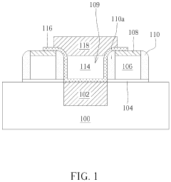
Vertical oxide-semiconductor transistor and method of manufacturing the same
PatentActiveUS20230361218A1
Innovation
- A vertical oxide-semiconductor transistor design with a gate that surrounds the source and forms a recess, featuring an inner spacer and oxide-semiconductor layer, and a drain that completely covers the source and partially overlaps the gate, reducing the transistor area and Miller capacitance.
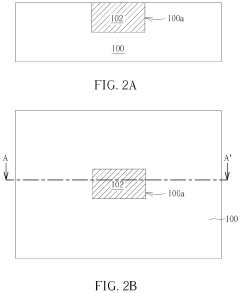
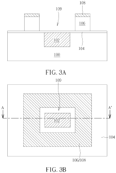
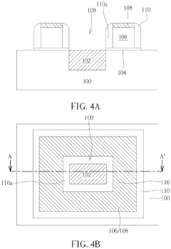
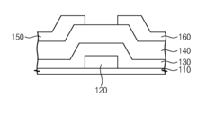
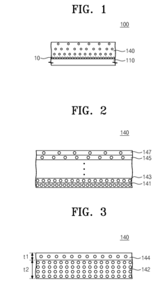
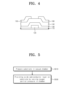
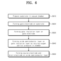
Oxide semiconductor device and method for manufacturing same
PatentActiveUS20160163867A1
Innovation
- A method involving a substrate with an oxide semiconductor layer having different oxygen vacancy concentrations, achieved by varying oxygen partial pressure during deposition, which includes forming multiple oxide thin-films with varying thickness ratios and oxygen vacancy levels, and incorporating a gate electrode and source/drain electrodes to optimize device performance.
Environmental Impact and Sustainability of Semiconductor Materials
The semiconductor industry's environmental impact has become increasingly significant as global production volumes continue to rise. Silicon-based semiconductor manufacturing processes are notably resource-intensive, requiring substantial amounts of ultra-pure water, energy, and chemicals. A typical silicon fabrication facility consumes between 2-4 million gallons of water daily and uses various hazardous chemicals including hydrofluoric acid, sulfuric acid, and numerous solvents that pose environmental risks if not properly managed.
In contrast, oxide semiconductor manufacturing generally demonstrates a more favorable environmental profile. These materials, particularly indium gallium zinc oxide (IGZO) and zinc oxide (ZnO), can be processed at significantly lower temperatures—often below 400°C compared to silicon's 1000°C+ requirements. This temperature differential translates to approximately 30-40% energy savings during manufacturing, with corresponding reductions in carbon emissions.
Material extraction considerations also favor oxide semiconductors in certain aspects. Silicon purification is extremely energy-intensive, requiring multiple refinement stages to achieve the 99.9999999% purity needed for electronics. While oxide semiconductors utilize some rare elements like indium, their overall material efficiency can be superior, with thinner active layers and fewer processing steps reducing material waste.
End-of-life management presents different challenges for both technologies. Silicon-based devices contain numerous toxic elements including arsenic, phosphorus, and boron dopants. Oxide semiconductors generally contain fewer toxic elements, though concerns exist regarding indium scarcity and extraction impacts. Recycling infrastructure for both technologies remains underdeveloped, with less than 20% of electronic waste currently recovered for material reuse.
Water usage metrics particularly favor oxide semiconductor production, with studies indicating potential reductions of 25-45% compared to traditional silicon manufacturing. This advantage becomes increasingly critical as semiconductor production expands in water-stressed regions globally.
Carbon footprint analyses across full product lifecycles show oxide semiconductor devices typically generate 15-30% less greenhouse gas emissions than equivalent silicon-based alternatives. This advantage stems primarily from lower processing temperatures and simplified manufacturing sequences, though the specific environmental benefits vary significantly depending on device type and application context.
Regulatory frameworks worldwide are increasingly prioritizing sustainable semiconductor manufacturing, with the EU's Restriction of Hazardous Substances (RoHS) directive and similar regulations in Asia and North America driving industry adoption of more environmentally responsible practices. These evolving standards may accelerate the transition toward oxide semiconductor technologies in applications where their performance characteristics are suitable.
Manufacturing Process Comparison and Scalability Assessment
The manufacturing processes for oxide semiconductor and silicon-based devices represent fundamentally different approaches with significant implications for production efficiency, cost structures, and scalability. Oxide semiconductors, particularly IGZO (Indium Gallium Zinc Oxide), can be deposited at significantly lower temperatures (typically below 300°C) compared to silicon processes that require temperatures exceeding 1000°C for high-quality crystallization.
This temperature difference translates directly to manufacturing advantages, as oxide semiconductor fabrication is compatible with a wider range of substrate materials, including flexible polymers that would degrade at silicon processing temperatures. The lower thermal budget also results in reduced energy consumption during manufacturing, contributing to both cost savings and environmental sustainability.
Deposition methods for oxide semiconductors primarily involve sputtering techniques, which can be performed using standard equipment with relatively straightforward process control. In contrast, silicon-based devices require complex epitaxial growth processes, ion implantation, and multiple high-temperature annealing steps, necessitating sophisticated clean room environments and specialized equipment.
From a scalability perspective, oxide semiconductor manufacturing demonstrates superior characteristics for large-area applications. The uniform deposition achievable with sputtering techniques enables consistent performance across large substrates, making oxide semiconductors particularly suitable for large display panels. Silicon manufacturing, while highly refined for integrated circuits, faces challenges when scaling to larger areas due to crystallization uniformity issues.
The material supply chain represents another critical manufacturing consideration. Silicon is abundant and has a well-established supply chain, whereas oxide semiconductors often incorporate indium and gallium, which face potential supply constraints. This material availability factor could impact long-term scalability and cost structures as production volumes increase.
Defect density and yield rates also differ significantly between the two technologies. Oxide semiconductor processes typically achieve lower defect densities in large-area applications, contributing to higher manufacturing yields. Silicon processes, while capable of extremely high integration densities, tend to experience yield challenges as device dimensions shrink below certain thresholds.
Manufacturing equipment depreciation schedules and capital expenditure requirements favor oxide semiconductor production, with generally lower initial investment requirements and less frequent equipment replacement cycles. This economic advantage becomes particularly significant when considering market entry barriers for new manufacturing facilities.
Unlock deeper insights with Patsnap Eureka Quick Research — get a full tech report to explore trends and direct your research. Try now!
Generate Your Research Report Instantly with AI Agent
Supercharge your innovation with Patsnap Eureka AI Agent Platform!