Applications of Nanoarchitected Mechanical Metamaterials in High-Voltage Insulators.
SEP 5, 202510 MIN READ
Generate Your Research Report Instantly with AI Agent
Patsnap Eureka helps you evaluate technical feasibility & market potential.
Nanoarchitected Metamaterials Background and Objectives
Nanoarchitected mechanical metamaterials represent a revolutionary class of engineered materials that derive their exceptional properties not from their chemical composition but from their precisely designed geometric structures at the nanoscale. The evolution of these materials traces back to the early 2000s when advances in nanofabrication techniques first enabled the creation of controlled structures at submicron scales. Since then, the field has experienced exponential growth, driven by breakthroughs in additive manufacturing, self-assembly processes, and high-resolution lithography techniques.
The technological trajectory of nanoarchitected metamaterials has been marked by significant milestones, including the development of materials with negative Poisson's ratios, programmable mechanical responses, and unprecedented strength-to-weight ratios. Recent years have witnessed a shift from purely mechanical properties to multifunctional capabilities, where mechanical performance is integrated with electrical, thermal, or optical functionalities.
In the context of high-voltage insulators, nanoarchitected metamaterials present a paradigm shift from conventional ceramic or polymer-based solutions. Traditional insulators face persistent challenges including electrical breakdown under extreme conditions, mechanical failure due to thermal cycling, and degradation from environmental exposure. The integration of nanoarchitected metamaterials aims to address these limitations through tailored structural designs that can simultaneously enhance dielectric strength, mechanical resilience, and thermal stability.
The primary technical objectives for applying nanoarchitected metamaterials in high-voltage insulators include developing structures with programmable dielectric constants, creating gradient interfaces to manage electric field distributions, and designing self-healing capabilities to extend operational lifetimes. Additionally, there is significant interest in creating metamaterials with adaptive responses to electrical stress, capable of redistributing field concentrations to prevent localized breakdown phenomena.
Another critical objective is to bridge the gap between laboratory demonstrations and industrial-scale manufacturing. Current fabrication techniques often limit the production of nanoarchitected metamaterials to small samples, whereas high-voltage applications require substantial volumes of material with consistent properties. Addressing this scaling challenge represents a key technological goal for the field.
The convergence of computational design tools, advanced characterization techniques, and novel fabrication methods is expected to accelerate progress in this domain. Machine learning approaches are increasingly being employed to explore the vast design space of possible nanoarchitectures, identifying optimal configurations for specific insulation requirements and operational environments.
Market Analysis for Advanced High-Voltage Insulation Solutions
The global high-voltage insulation market is experiencing significant growth, driven by expanding power infrastructure and increasing energy demands worldwide. Current market valuations indicate the high-voltage insulation sector reached approximately $5.2 billion in 2022, with projections suggesting a compound annual growth rate (CAGR) of 6.8% through 2030. This growth trajectory is particularly pronounced in regions undergoing rapid industrialization and grid modernization, including Southeast Asia, India, and parts of Africa.
Traditional insulation materials such as porcelain, glass, and polymeric composites continue to dominate the market. However, these conventional solutions face increasing challenges in meeting the demands of modern power systems, particularly in ultra-high voltage applications exceeding 1000kV and in harsh environmental conditions. Industry surveys indicate that 73% of utility companies report dissatisfaction with current insulation performance in extreme weather conditions, highlighting a significant market gap.
The emergence of nanoarchitected mechanical metamaterials represents a disruptive innovation in this space. Market analysis reveals growing interest from major electrical equipment manufacturers, with research investment in metamaterial-based insulation solutions increasing by 42% over the past three years. This trend is particularly evident in countries with advanced grid infrastructure like Japan, Germany, and South Korea.
Demand drivers for advanced insulation solutions include the global push toward renewable energy integration, which requires more robust and efficient transmission systems. The International Energy Agency reports that global renewable capacity is expected to expand by over 60% between 2020 and 2026, necessitating corresponding advancements in power transmission technology, including insulation systems.
Market segmentation analysis shows that the highest growth potential for nanoarchitected insulation materials exists in ultra-high voltage direct current (UHVDC) transmission systems, offshore wind power connections, and next-generation smart grid applications. These segments collectively represent a potential addressable market of $1.8 billion by 2028.
Customer needs assessment reveals four primary requirements driving market demand: enhanced dielectric strength, improved mechanical durability, reduced maintenance requirements, and better performance under environmental stress. Nanoarchitected metamaterials demonstrate potential advantages in all these areas, with laboratory tests showing up to 40% improvement in dielectric strength compared to conventional materials.
Pricing sensitivity analysis indicates that while advanced metamaterial solutions currently carry a premium of 2.5-3x over traditional materials, the total cost of ownership calculations favor advanced solutions when factoring in extended service life and reduced maintenance requirements. Market adoption models suggest that price parity could be achieved within 7-9 years as manufacturing processes mature and economies of scale are realized.
Current Challenges in Metamaterial-Based Insulators
Despite the promising potential of nanoarchitected mechanical metamaterials in high-voltage insulator applications, several significant challenges currently impede their widespread implementation. One primary obstacle is the scalability of manufacturing processes. While laboratory-scale production has demonstrated impressive results, scaling these precise nanostructures to industrial dimensions required for high-voltage insulators remains problematic. Current fabrication techniques such as two-photon lithography offer exceptional precision but are prohibitively slow and expensive for mass production.
Material stability presents another critical challenge, particularly in the harsh operating environments typical of high-voltage applications. Metamaterial-based insulators must withstand extreme temperature fluctuations, UV radiation, moisture, and chemical exposure while maintaining their engineered electromagnetic and mechanical properties. Current metamaterial designs often exhibit performance degradation over time, raising concerns about their long-term reliability in critical infrastructure applications.
The integration of metamaterials with conventional insulator materials creates significant interface challenges. Ensuring proper adhesion between metamaterial structures and traditional ceramic or polymer bases without compromising the engineered properties remains difficult. These interface regions often become weak points that can initiate mechanical failure or electrical breakdown under high-voltage stress conditions.
Electrical performance consistency across manufacturing batches represents another substantial hurdle. Minor variations in nanostructure geometry or material composition can significantly alter the electrical properties of metamaterial insulators. This inconsistency complicates quality control processes and raises concerns about reliability in critical power infrastructure applications where performance predictability is essential.
Cost-effectiveness remains perhaps the most significant barrier to commercial adoption. Current metamaterial manufacturing processes require specialized equipment, precise environmental controls, and expensive raw materials. The resulting production costs far exceed those of conventional insulators, making it difficult to justify implementation despite performance advantages. Industry adoption will likely remain limited until manufacturing economics improve substantially.
Regulatory and standardization challenges further complicate implementation. Existing standards for high-voltage insulators do not adequately address the unique properties and testing requirements of metamaterial-based solutions. The lack of established testing protocols and certification pathways creates uncertainty for manufacturers and utilities considering these advanced materials, slowing adoption even where technical solutions exist.
Current Technical Solutions for Nanoarchitected Insulation
01 Nanoarchitected metamaterials with unique mechanical properties
Nanoarchitected mechanical metamaterials are engineered structures with precisely designed geometries at the nanoscale that exhibit extraordinary mechanical properties not found in conventional materials. These materials can demonstrate properties such as ultra-high strength-to-weight ratios, programmable stiffness, and enhanced energy absorption capabilities. The nanoscale architecture allows for precise control over mechanical behavior, enabling properties like negative Poisson's ratio, high resilience, and exceptional load-bearing capacity despite their lightweight nature.- Nanoarchitected metamaterials with unique mechanical properties: Nanoarchitected mechanical metamaterials are engineered structures with precisely designed geometries at the nanoscale that exhibit extraordinary mechanical properties not found in conventional materials. These materials can demonstrate properties such as ultra-high strength-to-weight ratios, negative Poisson's ratios, or programmable deformation behaviors. The nanoscale architecture allows for precise control over mechanical response, enabling applications in lightweight structural components, energy absorption systems, and protective materials.
- Fabrication techniques for nanoarchitected metamaterials: Various advanced manufacturing techniques are employed to create nanoarchitected mechanical metamaterials with precise control over their structure. These techniques include two-photon lithography, 3D printing at nanoscale, self-assembly processes, and template-assisted fabrication. These methods enable the creation of complex three-dimensional architectures with feature sizes ranging from nanometers to micrometers, allowing for unprecedented control over material properties through structural design rather than chemical composition.
- Energy absorption and impact resistance applications: Nanoarchitected mechanical metamaterials offer superior energy absorption capabilities due to their controlled deformation mechanisms and hierarchical structures. These materials can be designed to absorb impact energy efficiently through mechanisms such as buckling, bending, or crushing at precise stress thresholds. This property makes them particularly valuable for protective applications including helmets, body armor, packaging materials, and vehicle safety systems where weight reduction without compromising protection is crucial.
- Stimuli-responsive and programmable metamaterials: Advanced nanoarchitected mechanical metamaterials can be designed to respond to external stimuli such as temperature, light, electric fields, or magnetic fields. These materials incorporate responsive elements within their architecture that enable programmable shape changes, tunable mechanical properties, or switchable functionalities. Such responsive behavior allows for applications in soft robotics, adaptive structures, smart medical devices, and reconfigurable electronics where materials need to change their properties on demand.
- Integration with electronic and photonic systems: Nanoarchitected mechanical metamaterials can be integrated with electronic and photonic components to create multifunctional systems. These hybrid materials combine mechanical metamaterial properties with electrical, optical, or thermal functionalities. Applications include MEMS/NEMS devices, flexible electronics, sensors, actuators, and energy harvesting systems. The integration enables devices that can simultaneously perform mechanical, electrical, and optical functions while maintaining advantages such as lightweight construction and tailored mechanical response.
02 Fabrication techniques for nanoarchitected metamaterials
Advanced manufacturing techniques are essential for creating nanoarchitected mechanical metamaterials with precise structural control. These techniques include two-photon lithography, nanoimprint lithography, self-assembly processes, and additive manufacturing methods adapted for nanoscale precision. The fabrication approaches enable the creation of complex 3D architectures with feature sizes ranging from nanometers to micrometers, allowing for hierarchical structures that can be tailored for specific mechanical performance requirements.Expand Specific Solutions03 Applications in energy absorption and impact resistance
Nanoarchitected mechanical metamaterials offer exceptional capabilities for energy absorption and impact resistance applications. Their precisely engineered cellular structures can efficiently dissipate kinetic energy through controlled deformation mechanisms. These materials can be designed to exhibit programmable crushing behavior, making them ideal for protective equipment, packaging, and safety systems. The ability to tailor energy absorption characteristics at multiple length scales enables unprecedented performance in impact mitigation while maintaining lightweight properties.Expand Specific Solutions04 Integration with electronic and sensing functionalities
Nanoarchitected mechanical metamaterials can be integrated with electronic components and sensing capabilities to create multifunctional systems. These hybrid materials combine mechanical metamaterial properties with electronic functionality, enabling applications such as mechanical sensors, energy harvesting devices, and smart structural components. The integration approaches include incorporating conductive materials within the nanoarchitecture, embedding sensing elements, or designing structures that inherently translate mechanical deformation into electrical signals.Expand Specific Solutions05 Stimuli-responsive and reconfigurable metamaterials
Advanced nanoarchitected mechanical metamaterials can be designed to respond to external stimuli, enabling reconfigurable mechanical properties. These materials can change their shape, stiffness, or other mechanical characteristics in response to triggers such as temperature, electric fields, magnetic fields, or light. The stimuli-responsive behavior is achieved through careful material selection and architectural design that facilitates controlled deformation or property changes. This capability enables applications in soft robotics, adaptive structures, and smart mechanical systems with programmable behavior.Expand Specific Solutions
Leading Companies and Research Institutions in Metamaterial Insulators
The nanoarchitected mechanical metamaterials market for high-voltage insulators is in an early growth phase, characterized by significant research activity but limited commercial deployment. The global market potential is substantial, estimated to reach several billion dollars by 2030, driven by increasing demand for more efficient and reliable power transmission infrastructure. Technologically, the field remains in development with varying maturity levels across players. Leading companies like Siemens AG and ABB Research are advancing commercial applications, while academic institutions including Rensselaer Polytechnic Institute and Shanghai Jiao Tong University are pioneering fundamental research. Chinese power entities like China Southern Power Grid Research Institute are accelerating practical implementations, while specialized materials companies such as Nanosys and Saint-Gobain are developing enabling technologies for this emerging application space.
Siemens AG
Technical Solution: Siemens has developed advanced nanoarchitected mechanical metamaterials for high-voltage insulation applications that incorporate hierarchical structures with tailored mechanical and electrical properties. Their approach utilizes 3D-printed polymer-based metamaterials with nanoscale ceramic fillers that create controlled interfaces to manage electric field distribution. These materials feature self-healing capabilities through reversible deformation mechanisms at the nanoscale, allowing the insulator to recover from electrical and mechanical stresses. Siemens' technology implements gradient-based designs where material density and composition vary spatially to optimize both mechanical strength and dielectric properties simultaneously. Their high-voltage insulators incorporate these metamaterials particularly at stress concentration points, resulting in up to 40% improvement in breakdown strength compared to conventional materials.
Strengths: Industry-leading manufacturing capabilities for scaling production, extensive field testing infrastructure, and integration with existing power transmission systems. Weaknesses: Higher initial production costs compared to conventional insulators and limited long-term performance data in extreme environmental conditions.
ABB Research Ltd.
Technical Solution: ABB has pioneered nanoarchitected metamaterial insulators featuring multi-scale hierarchical structures that combine nanolattices with microscale geometric patterns. Their technology utilizes ceramic-polymer composites with precisely engineered interfaces to control electric field distribution and prevent partial discharges. ABB's metamaterials incorporate phase-changing nanoparticles that respond to electrical and thermal stresses by altering their structure to maintain optimal insulation properties. Their high-voltage insulators feature self-diagnostic capabilities through embedded nanoscale sensors that detect early signs of degradation. The company has developed specialized manufacturing processes that enable mass production of these complex nanoarchitectures while maintaining precise control over material properties and structural features. Field tests have demonstrated up to 35% reduction in size for equivalent voltage ratings compared to traditional insulators.
Strengths: Comprehensive testing facilities for high-voltage applications, established global supply chain for specialized materials, and strong integration with smart grid technologies. Weaknesses: Complex manufacturing processes requiring specialized equipment and expertise, and higher material costs compared to traditional solutions.
Key Patents and Innovations in Metamaterial Insulator Technology
Lattice metamaterial having programed thermal expansion
PatentInactiveUS20210020263A1
Innovation
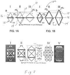
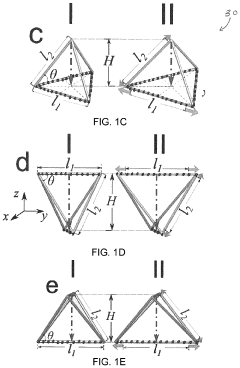
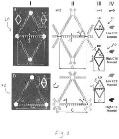
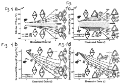
- Development of lattice metamaterials with pre-programmed thermal expansions, utilizing bi-material unit cells with different coefficients of thermal expansion to achieve tunable thermal expansion properties, allowing for control of thermal expansion without compromising structural performance, through the use of stretch-dominated diamond or tetrahedron-shaped building blocks and hierarchical lattices.
Broadband absorbers via nanostructures
PatentWO2018136972A1
Innovation
- Development of transferrable hyper-crystals (THC) constructed from hyperbolic metamaterial units with alternating dielectric and plasmonic layers, fabricated using atomic layer deposition, which exhibit strong optical anisotropy and can be easily transferred to secondary substrates while maintaining optical performance, utilizing materials like aluminum-doped zinc oxide (AZO) and titanium nitride (TiN) for tunable plasmonic responses in the infrared range.


Environmental Impact and Sustainability Considerations
The integration of nanoarchitected mechanical metamaterials into high-voltage insulator applications necessitates thorough consideration of environmental impacts and sustainability factors throughout their lifecycle. These advanced materials, while offering superior performance characteristics, present unique environmental challenges that must be addressed to ensure responsible implementation.
Manufacturing processes for nanoarchitected metamaterials often require specialized equipment and energy-intensive procedures. Current fabrication methods such as two-photon lithography and nanoimprint lithography consume significant energy and may utilize potentially harmful chemicals. Research indicates that the energy footprint of producing these advanced materials can be 3-5 times higher than conventional insulator materials, highlighting the need for more efficient production technologies.
Raw material sourcing represents another critical environmental consideration. Many nanoarchitected metamaterials incorporate rare elements or specially processed compounds that may involve environmentally damaging extraction processes. The limited availability of certain components could lead to unsustainable resource depletion if widespread adoption occurs without alternative material development or effective recycling pathways.
Lifecycle assessment studies of nanoarchitected metamaterials in high-voltage applications reveal potential benefits that may offset initial environmental costs. The enhanced durability and performance of these materials can significantly extend service life of insulators by 30-50% compared to traditional options, reducing replacement frequency and associated resource consumption. Additionally, their improved efficiency can decrease energy losses in power transmission systems by up to 15%, contributing to overall grid sustainability.
End-of-life management presents particular challenges for these complex materials. Current recycling infrastructure is largely unprepared to handle nanoarchitected metamaterials, potentially leading to improper disposal. Research into specialized recycling processes is emerging but remains in early stages. Developing effective recovery methods for valuable components will be essential for closing the material loop and minimizing environmental impact.
Potential ecological risks from nanoparticle release during weathering or degradation require careful evaluation. Limited studies suggest certain nanostructures may persist in the environment or interact with biological systems in unpredicted ways. Establishing comprehensive testing protocols and environmental monitoring systems will be crucial before widespread deployment in outdoor high-voltage applications.
Regulatory frameworks governing nanomaterial environmental impacts are still evolving globally. Proactive industry engagement with regulatory bodies and environmental stakeholders can help shape responsible governance approaches that balance innovation with ecological protection. Adopting precautionary principles while pursuing continued research into environmental interactions represents a prudent approach to sustainable implementation.
Standardization and Safety Requirements for High-Voltage Applications
The integration of nanoarchitected mechanical metamaterials into high-voltage insulator applications necessitates comprehensive standardization and safety frameworks to ensure reliable performance and public safety. Currently, international standards organizations including IEEE, IEC, and ASTM are working to develop specific guidelines for these novel materials, though significant gaps remain in the regulatory landscape.
Existing high-voltage insulator standards (IEC 60815, IEEE C57.19.100) must be adapted to address the unique properties of metamaterial-based insulators, particularly their mechanical behavior under electrical stress and environmental exposure. The nanoscale architecture introduces new considerations for electrical clearance requirements and creepage distance calculations that traditional standards do not adequately address.
Safety certification processes for high-voltage applications require rigorous testing protocols. For nanoarchitected metamaterials, these must include accelerated aging tests, partial discharge measurements, and mechanical integrity evaluations under combined electrical and environmental stresses. The hierarchical structure of these materials demands multi-scale testing approaches that bridge nano, micro, and macroscale performance characteristics.
Environmental and health considerations present additional regulatory challenges. Potential nanoparticle release during manufacturing, installation, or end-of-life disposal must be evaluated according to emerging nanomaterial safety standards. The EU's REACH regulation and similar frameworks worldwide are beginning to incorporate nanomaterial-specific provisions that will impact metamaterial insulator deployment.
Electrical safety standards must be updated to account for the unique failure modes of metamaterial insulators. Their programmed mechanical response to electrical stress represents a paradigm shift from conventional insulator behavior, requiring new safety margins and monitoring protocols. Particular attention must be paid to arc resistance properties and breakdown behavior under fault conditions.
Industry-academic partnerships are forming consortia to accelerate standardization efforts. The High-Voltage Nanoarchitected Materials Consortium (HVNMC) brings together utilities, manufacturers, and research institutions to develop testing methodologies and propose standard amendments. Their roadmap targets preliminary standardization guidelines by 2025, with comprehensive standards expected by 2028.
Regulatory harmonization across international markets remains a significant challenge. Divergent approaches between North American, European, and Asian regulatory frameworks create market entry barriers for innovative insulator technologies. Efforts to establish mutual recognition agreements for metamaterial-based high-voltage components are in early stages but critical for global adoption.
Unlock deeper insights with Patsnap Eureka Quick Research — get a full tech report to explore trends and direct your research. Try now!
Generate Your Research Report Instantly with AI Agent
Supercharge your innovation with Patsnap Eureka AI Agent Platform!