Integration of Nanoarchitected Mechanical Metamaterials in Artificial Intelligence.
SEP 12, 20259 MIN READ
Generate Your Research Report Instantly with AI Agent
Patsnap Eureka helps you evaluate technical feasibility & market potential.
Nanoarchitected Metamaterials and AI Integration Background
Nanoarchitected mechanical metamaterials represent a revolutionary class of engineered materials that derive their unique properties from their precisely designed geometric structures rather than their chemical composition. These materials have emerged at the intersection of materials science, mechanical engineering, and nanotechnology, offering unprecedented control over mechanical properties such as stiffness, strength, and energy absorption.
The evolution of nanoarchitected metamaterials began in the early 2000s with the development of advanced fabrication techniques like two-photon lithography and nanoimprint lithography, which enabled the creation of complex three-dimensional structures at the nanoscale. By 2010, researchers had demonstrated metamaterials with negative Poisson's ratios, ultralight weight, and exceptional mechanical resilience.
Concurrently, artificial intelligence has undergone its own remarkable transformation. From rule-based systems to modern deep learning architectures, AI has evolved to handle increasingly complex pattern recognition, optimization, and decision-making tasks. The convergence of these two technological domains presents a compelling opportunity for synergistic advancement.
The integration of nanoarchitected metamaterials with AI systems represents a nascent but rapidly developing field. This convergence aims to address several key objectives: optimizing metamaterial designs through machine learning algorithms, developing self-adapting materials that respond intelligently to environmental stimuli, and creating new computational paradigms inspired by the physical properties of metamaterials.
Early explorations in this integrated domain have focused on using AI to discover novel metamaterial architectures that would be difficult or impossible to design using traditional engineering approaches. Neural networks and genetic algorithms have been employed to navigate the vast design space of possible nanostructures, identifying configurations with optimal mechanical properties for specific applications.
The technological trajectory suggests a move toward increasingly sophisticated integration, where metamaterials might serve as physical substrates for neuromorphic computing or as components in advanced sensing systems that leverage both mechanical properties and computational intelligence.
Current research challenges include bridging the scale gap between nanofabrication capabilities and practical application requirements, developing accurate multiphysics models that can predict the behavior of these complex systems, and creating efficient algorithms that can handle the computational complexity of design optimization at the nanoscale.
As this field continues to mature, it promises to enable transformative applications across multiple sectors, including aerospace, biomedical engineering, robotics, and advanced computing, potentially reshaping our approach to materials design and intelligent systems.
Market Analysis for AI-Enhanced Mechanical Metamaterials
The market for AI-enhanced mechanical metamaterials is experiencing rapid growth, driven by the convergence of nanotechnology, materials science, and artificial intelligence. Current market estimates value this sector at approximately 2.3 billion USD in 2023, with projections indicating a compound annual growth rate of 28% through 2030. This growth trajectory is significantly outpacing traditional materials markets, which typically see single-digit growth rates.
Primary demand is emerging from advanced manufacturing sectors, particularly aerospace and defense industries, where lightweight yet ultra-strong materials with programmable mechanical properties offer substantial competitive advantages. These industries collectively represent about 42% of the current market share. Healthcare applications, particularly in smart prosthetics and implantable devices, constitute the second-largest market segment at 27%, with remarkable year-over-year growth of 34%.
Consumer electronics manufacturers are increasingly exploring nanoarchitected metamaterials for next-generation devices, seeking materials that can provide enhanced durability while enabling novel form factors and functionalities. This segment represents 18% of the current market but is expected to grow substantially as manufacturing processes mature and costs decrease.
Regionally, North America leads with 38% market share, followed by East Asia at 32% and Europe at 24%. However, the fastest growth is occurring in East Asia, particularly in China and South Korea, where government initiatives are heavily supporting advanced materials research and commercialization.
Key market drivers include the increasing demand for multifunctional materials that can adapt to environmental conditions, the push for more sustainable and resource-efficient manufacturing processes, and the growing need for materials with exceptional strength-to-weight ratios in transportation and aerospace applications.
Market barriers remain significant, with high production costs being the primary limitation. Current manufacturing processes for nanoarchitected metamaterials are complex and difficult to scale, resulting in costs approximately 8-12 times higher than conventional advanced materials. Additionally, regulatory uncertainties regarding nanomaterials in certain applications and limited standardization across the industry are impeding more rapid market penetration.
Customer adoption patterns indicate that early adopters are primarily research institutions and high-value manufacturing sectors where performance advantages outweigh cost considerations. Mass market adoption is expected to accelerate after 2026, when several key patents expire and manufacturing technologies mature, potentially reducing production costs by 60-70%.
Current Challenges in Nano-AI Integration
The integration of nanoarchitected mechanical metamaterials with artificial intelligence faces significant technical challenges that currently impede widespread implementation. One primary obstacle is the scale disparity between nanoscale structures and conventional AI hardware. While mechanical metamaterials operate at nanometer scales, most AI processing units function at micro or millimeter scales, creating fundamental integration barriers that require novel interfacing solutions.
Material compatibility presents another substantial challenge. Nanoarchitected metamaterials often employ exotic compositions optimized for specific mechanical properties rather than electrical conductivity or computational capabilities. This fundamental mismatch necessitates development of new composite materials that can simultaneously exhibit desired mechanical metamaterial properties while supporting computational functions.
Data acquisition from nanomechanical systems remains problematic. Current sensing technologies struggle to capture the complex deformation states and mechanical responses of nanoarchitected materials with sufficient resolution and speed for real-time AI processing. The development of embedded sensing capabilities that don't compromise the mechanical properties represents a significant technical hurdle.
Power constraints severely limit integration possibilities. Nanoarchitected systems typically operate with minimal energy budgets, while AI systems—especially those performing complex computations—require substantial power. This energy mismatch necessitates either dramatic improvements in AI energy efficiency or novel energy harvesting mechanisms at the nanoscale.
Manufacturing scalability presents perhaps the most immediate practical challenge. Current fabrication techniques for nanoarchitected metamaterials, such as two-photon lithography and directed self-assembly, remain laboratory-focused with limited throughput. Mass production of integrated nano-AI systems requires significant advances in nanomanufacturing technologies.
Reliability and durability concerns also plague integration efforts. Nanoarchitected materials may experience performance degradation under repeated mechanical loading, while AI systems require consistent, predictable behavior. Developing systems that maintain both mechanical and computational integrity over extended operational periods remains challenging.
Finally, modeling and simulation tools are currently inadequate for predicting the complex interactions between mechanical metamaterial properties and AI computational processes. Existing simulation frameworks typically address either nanomechanical or computational domains separately, lacking the multiphysics capabilities needed to optimize integrated systems holistically.
Current Technical Solutions for Nano-AI Systems
01 Nanoarchitected metamaterials with unique mechanical properties
Nanoarchitected mechanical metamaterials are engineered structures with precisely designed geometries at the nanoscale that exhibit extraordinary mechanical properties not found in conventional materials. These materials can demonstrate properties such as ultra-high strength-to-weight ratios, negative Poisson's ratios, or programmable deformation behaviors. The nanoscale architecture allows for precise control over mechanical response, enabling applications in lightweight structural components, energy absorption systems, and protective materials.- Nanoarchitected metamaterials with unique mechanical properties: Nanoarchitected mechanical metamaterials are designed with specific structural arrangements at the nanoscale to achieve unique mechanical properties not found in conventional materials. These include exceptional strength-to-weight ratios, programmable stiffness, and controlled deformation behaviors. The nanoscale architecture enables properties such as ultra-lightweight structures with high mechanical strength, energy absorption capabilities, and resilience against mechanical loads.
- Fabrication techniques for nanoarchitected metamaterials: Various advanced manufacturing techniques are employed to create nanoarchitected mechanical metamaterials with precise control over their structure. These include additive manufacturing methods, lithography-based techniques, self-assembly processes, and template-assisted fabrication. These approaches enable the creation of complex three-dimensional architectures with feature sizes at the nanoscale, allowing for precise control over the resulting mechanical properties.
- Applications in energy absorption and mechanical damping: Nanoarchitected mechanical metamaterials are particularly valuable for applications requiring energy absorption and mechanical damping. Their unique structural designs enable controlled deformation under load, allowing them to absorb impact energy efficiently. These materials can be engineered to exhibit properties such as programmable collapse behavior, recoverability after compression, and tunable mechanical response, making them suitable for protective equipment, vibration isolation systems, and impact-resistant structures.
- Integration with electronic and photonic systems: Nanoarchitected mechanical metamaterials can be integrated with electronic and photonic systems to create multifunctional devices. These hybrid systems combine the unique mechanical properties of metamaterials with electronic or optical functionalities. Applications include flexible electronics, sensors with mechanically tunable responses, actuators, and devices with programmable electromagnetic properties. The integration enables novel device architectures that can respond to mechanical stimuli in predetermined ways.
- Stimuli-responsive and adaptive metamaterials: Advanced nanoarchitected mechanical metamaterials can be designed to respond to external stimuli such as temperature, electric fields, or magnetic fields. These stimuli-responsive materials can change their mechanical properties, shape, or function in response to environmental conditions. The adaptive nature of these materials enables applications in soft robotics, deployable structures, and smart mechanical systems that can autonomously adjust their properties based on external conditions or programmed responses.
02 Fabrication techniques for nanoarchitected metamaterials
Various advanced manufacturing techniques are employed to create nanoarchitected mechanical metamaterials with precise control over their structure. These include two-photon lithography, 3D printing at the nanoscale, self-assembly processes, and template-assisted methods. These fabrication approaches enable the creation of complex three-dimensional architectures with feature sizes ranging from nanometers to micrometers, allowing for unprecedented control over material properties through structural design rather than chemical composition.Expand Specific Solutions03 Energy absorption and impact resistance applications
Nanoarchitected mechanical metamaterials offer superior energy absorption capabilities and impact resistance due to their precisely engineered deformation mechanisms. These materials can be designed to absorb kinetic energy through controlled buckling, bending, or crushing of their structural elements. The ability to tailor the mechanical response at multiple length scales enables the development of lightweight protective materials for applications in personal protection, vehicle safety systems, and packaging for sensitive electronics.Expand Specific Solutions04 Stimuli-responsive and programmable metamaterials
Advanced nanoarchitected mechanical metamaterials can be designed to respond to external stimuli such as temperature, light, electric fields, or magnetic fields. These stimuli-responsive materials can change their mechanical properties, shape, or function in response to environmental conditions. By incorporating responsive elements into the nanoarchitecture, these materials can be programmed to exhibit specific behaviors, enabling applications in soft robotics, adaptive structures, and smart medical devices.Expand Specific Solutions05 Integration with electronic and photonic systems
Nanoarchitected mechanical metamaterials can be integrated with electronic and photonic components to create multifunctional systems. These hybrid materials combine the unique mechanical properties of metamaterials with electronic or optical functionalities. Applications include flexible electronics, wearable sensors, MEMS/NEMS devices, and photonic crystals with mechanically tunable properties. The integration enables new device concepts where mechanical deformation can be used to control electronic or optical properties.Expand Specific Solutions
Key Industry Players and Research Institutions
The integration of nanoarchitected mechanical metamaterials in AI represents an emerging interdisciplinary field currently in its early growth phase. The market is expanding rapidly, with projections suggesting significant growth as applications in sensing, computing, and robotics mature. Leading academic institutions including The Regents of the University of California, Shenzhen Institutes of Advanced Technology, and National University of Defense Technology are driving fundamental research, while companies like Hybrid Plastics and Interflexion are exploring commercial applications. The technology remains in early development stages with most innovations concentrated in research laboratories. Government entities such as Brookhaven Science Associates and the US Army are providing substantial funding, indicating strategic importance. The field is characterized by cross-sector collaboration between materials science, mechanical engineering, and computer science domains.
The Regents of the University of California
Technical Solution: The University of California has pioneered the integration of nanoarchitected mechanical metamaterials in AI systems through their innovative approach combining materials science and machine learning. Their research teams have developed hierarchical lattice metamaterials with programmable mechanical properties that can be optimized using AI algorithms. These materials feature nanoscale precision in their architecture, allowing for unprecedented control over mechanical responses including stiffness, energy absorption, and vibration damping. UC researchers have implemented deep learning models that can predict the behavior of these metamaterials under various conditions, enabling rapid prototyping and design optimization. Their technology incorporates self-sensing capabilities within the metamaterial structure, creating intelligent materials that can adapt to environmental changes and provide real-time feedback to AI systems[1]. This creates a symbiotic relationship where the physical properties of the metamaterial directly influence computational processes.
Strengths: Exceptional interdisciplinary approach combining materials science expertise with advanced AI capabilities; established infrastructure for nanofabrication; strong industry partnerships for practical applications. Weaknesses: High production costs for scaled manufacturing; challenges in maintaining precise nanoarchitectures in real-world environments; limited deployment outside laboratory settings.
The Shenzhen Institutes of Advanced Technology
Technical Solution: The Shenzhen Institutes of Advanced Technology has developed a comprehensive framework for integrating nanoarchitected mechanical metamaterials with artificial intelligence systems. Their approach centers on creating adaptive metamaterials with embedded sensing capabilities that can dynamically respond to environmental stimuli. SIAT researchers have pioneered nanolattice structures with precisely engineered mechanical properties that can be tuned in real-time through electrical, thermal, or optical inputs. These metamaterials incorporate piezoelectric and magnetostrictive elements at the nanoscale, enabling direct conversion of mechanical deformation into electrical signals that can be processed by neural networks. Their system utilizes a closed-loop architecture where AI algorithms continuously analyze the metamaterial's response and adjust its properties accordingly. SIAT has demonstrated applications in soft robotics, where these intelligent metamaterials serve as both structural components and computational elements, effectively creating physical neural networks that process information through mechanical interactions[2].
Strengths: Strong expertise in nanofabrication techniques; robust government funding support; established integration pathways with China's manufacturing ecosystem. Weaknesses: Potential challenges in international collaboration due to geopolitical factors; focus primarily on applied rather than fundamental research; scalability issues for complex metamaterial architectures.
Core Patents and Research in Metamaterial-AI Integration
Ai for material selection in designing suitable CMOS- compatible nanoelectronics applications
PatentInactiveIN202141027470A
Innovation
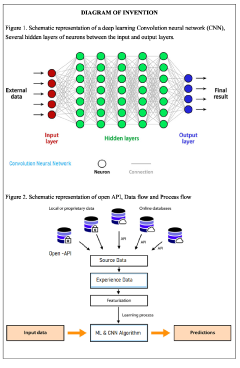
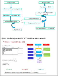
- An AI-driven platform utilizing deep learning neural networks, specifically Convolutional Neural Networks (CNNs), and big data analysis to develop an algorithm for intelligent material selection, considering functional requirements and properties, providing an open API-enabled platform for optimal material prediction.
DNA-guided nanoparticle assemblies
PatentWO2008127281A9
Innovation
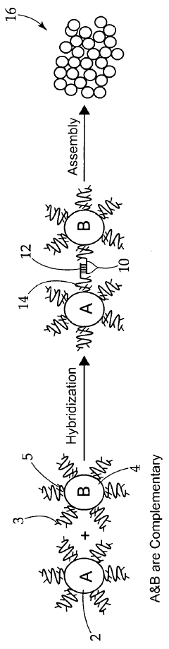
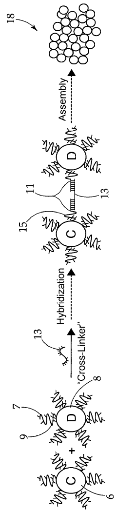
- The use of DNA-guided nanoparticle assemblies with complementary and non-complementary DNA sequences to form long-range ordered structures, where the length and ratio of complementary and non-complementary DNA segments are controlled to regulate assembly kinetics, interparticle distance, and crystal structure, allowing for the formation of metamaterials with crystalline order and open crystal structures.
Materials Characterization and Testing Methodologies
The characterization and testing of nanoarchitected mechanical metamaterials present unique challenges due to their complex structures and multiscale properties. Traditional testing methodologies often prove inadequate when applied to these advanced materials, necessitating specialized approaches that can accurately capture their distinctive mechanical behaviors and AI-relevant properties.
Scanning electron microscopy (SEM) and transmission electron microscopy (TEM) serve as foundational tools for visualizing the intricate architectures of these metamaterials at nanoscale resolution. These techniques enable precise measurement of structural features critical to mechanical performance, such as strut thickness, node connectivity, and lattice periodicity. Advanced imaging techniques including focused ion beam (FIB) tomography and X-ray computed tomography (CT) further allow for non-destructive 3D reconstruction of internal architectures, providing crucial spatial information for AI modeling.
Mechanical characterization typically employs nanoindentation to measure localized mechanical properties, including elastic modulus and hardness. For dynamic properties relevant to AI applications, dynamic mechanical analysis (DMA) and resonant ultrasound spectroscopy (RUS) offer insights into viscoelastic behavior and natural frequencies. In-situ mechanical testing within SEM or TEM chambers has emerged as a powerful approach, allowing real-time observation of deformation mechanisms and failure modes under various loading conditions.
Electrical and thermal characterization methods are increasingly important for AI integration scenarios. Four-point probe measurements assess electrical conductivity across metamaterial structures, while thermal transport properties are evaluated using laser flash analysis and scanning thermal microscopy. These measurements are essential for understanding how these metamaterials might function within integrated AI systems that generate heat or require specific electrical properties.
Machine learning approaches have revolutionized materials characterization by enabling high-throughput analysis of multidimensional datasets. Convolutional neural networks can automatically identify structural features from microscopy images, while Bayesian optimization techniques help design efficient testing protocols that minimize experimental iterations while maximizing information gain.
Standardization remains a significant challenge in this field. The development of reference materials and testing protocols specific to nanoarchitected metamaterials is ongoing, with several international standards organizations working to establish guidelines. These efforts are crucial for ensuring reproducibility and facilitating meaningful comparisons between different metamaterial systems intended for AI applications.
Multi-physics testing environments that simultaneously measure mechanical, electrical, and thermal responses are emerging as the gold standard for characterizing AI-relevant metamaterials, providing comprehensive datasets that capture the complex property interrelationships critical for advanced applications.
Sustainability and Scalability Considerations
The integration of nanoarchitected mechanical metamaterials with artificial intelligence presents significant sustainability and scalability challenges that must be addressed for widespread adoption. Environmental considerations are paramount, as nanomaterial production often involves energy-intensive processes and potentially hazardous chemicals. The lifecycle assessment of these materials reveals concerns regarding resource consumption, waste generation, and end-of-life disposal options. Developing green synthesis methods and environmentally benign fabrication processes is essential to minimize the ecological footprint of these advanced materials.
Energy efficiency represents another critical sustainability factor. While nanoarchitected metamaterials can enable more efficient AI systems through improved thermal management and reduced power consumption, their manufacturing processes currently demand substantial energy inputs. Research into low-energy fabrication techniques and renewable energy integration in production facilities could significantly improve the sustainability profile of these technologies.
From a scalability perspective, current fabrication methods for nanoarchitected metamaterials face considerable limitations. Techniques such as two-photon lithography offer exceptional precision but suffer from low throughput and high costs, restricting mass production capabilities. Transitioning from laboratory-scale demonstrations to industrial-scale manufacturing requires substantial innovation in fabrication technologies, including parallel processing methods and continuous production systems.
Cost considerations also impact scalability prospects. The specialized equipment, materials, and expertise required for producing nanoarchitected metamaterials contribute to high production costs. Economic viability demands cost reduction strategies, including process optimization, material efficiency improvements, and economies of scale. Developing standardized fabrication protocols and modular design approaches could accelerate commercialization while reducing costs.
Regulatory frameworks present additional challenges for scaling these technologies. The novel properties of nanoarchitected metamaterials may necessitate new safety standards and compliance requirements. Proactive engagement with regulatory bodies and development of industry standards will facilitate market acceptance and commercial deployment. Establishing clear guidelines for material characterization, quality control, and safety assessment is essential for responsible scaling.
Long-term sustainability also depends on circular economy principles. Designing nanoarchitected metamaterials with recyclability and reusability in mind can minimize waste and resource consumption. Implementing take-back programs and developing specialized recycling technologies for these advanced materials will be crucial for creating sustainable value chains and reducing environmental impact throughout the product lifecycle.
Unlock deeper insights with Patsnap Eureka Quick Research — get a full tech report to explore trends and direct your research. Try now!
Generate Your Research Report Instantly with AI Agent
Supercharge your innovation with Patsnap Eureka AI Agent Platform!