Directions in Nanoarchitected Mechanical Metamaterials for Sensor Technologies.
SEP 5, 202510 MIN READ
Generate Your Research Report Instantly with AI Agent
Patsnap Eureka helps you evaluate technical feasibility & market potential.
Nanoarchitected Metamaterials Background and Objectives
Nanoarchitected mechanical metamaterials represent a revolutionary frontier in materials science, emerging from the convergence of nanotechnology, mechanical engineering, and materials design. These engineered structures possess unique properties that transcend those of conventional materials, primarily due to their precisely designed architecture at the nanoscale rather than their chemical composition. The evolution of this field has been accelerated by advancements in nanofabrication techniques, computational modeling, and characterization methods over the past two decades.
The historical trajectory of nanoarchitected metamaterials began with theoretical frameworks in the early 2000s, followed by rudimentary experimental demonstrations. The field gained significant momentum around 2010 with the development of more sophisticated fabrication techniques such as two-photon lithography, allowing for unprecedented control over three-dimensional nanostructures. This technological progression has enabled the creation of materials with extraordinary mechanical properties, including negative Poisson's ratio, programmable stiffness, and exceptional strength-to-weight ratios.
Current research trends indicate a shift from purely mechanical properties toward multifunctional capabilities, particularly in sensing applications. The integration of mechanical metamaterials with sensing functionalities represents a natural evolution, leveraging their unique deformation characteristics, tunable resonant frequencies, and exceptional sensitivity to external stimuli. This convergence creates opportunities for next-generation sensors with unprecedented performance metrics.
The primary technical objectives in this domain include developing scalable fabrication methods for nanoarchitected sensor platforms, enhancing sensitivity and selectivity through architectural optimization, and achieving multifunctional sensing capabilities within single metamaterial structures. Additionally, there is a growing focus on creating self-powered and wireless sensing systems by incorporating energy harvesting mechanisms into the metamaterial architecture.
Another critical objective involves improving the durability and reliability of these materials under real-world operating conditions, addressing challenges related to environmental stability, fatigue resistance, and long-term performance. Researchers are also exploring bio-inspired designs to enhance functionality and adaptability, drawing inspiration from natural structures that have evolved sophisticated sensing mechanisms.
The ultimate goal of this technological trajectory is to establish nanoarchitected mechanical metamaterials as a versatile platform for next-generation sensing technologies across diverse applications, including healthcare monitoring, environmental sensing, structural health monitoring, and advanced manufacturing. This requires not only advancing the fundamental science but also developing practical engineering solutions that bridge the gap between laboratory demonstrations and commercial implementation.
Market Demand Analysis for Nano-Sensor Technologies
The global market for nano-sensor technologies is experiencing unprecedented growth, driven by increasing demand for miniaturized sensing solutions across multiple industries. Current market valuations place the nano-sensor sector at approximately $14.3 billion in 2023, with projections indicating a compound annual growth rate (CAGR) of 11.2% through 2030, potentially reaching $30.1 billion by the end of the decade.
Healthcare and biomedical applications represent the largest market segment, accounting for nearly 32% of the total nano-sensor market. The demand is primarily fueled by the need for continuous health monitoring, point-of-care diagnostics, and early disease detection capabilities. Nanoarchitected mechanical metamaterials offer exceptional sensitivity and specificity for detecting biomarkers at previously unattainable concentrations, creating significant opportunities for non-invasive diagnostic tools.
Environmental monitoring constitutes another rapidly expanding application area, growing at 13.5% annually. Industries and governments are increasingly investing in advanced sensing technologies to detect pollutants, monitor air and water quality, and ensure compliance with stricter environmental regulations. Nanoarchitected sensors provide advantages in terms of detection limits, response time, and the ability to operate in harsh environments.
The industrial sector demonstrates robust demand growth, particularly in structural health monitoring, predictive maintenance, and quality control applications. The unique mechanical properties of metamaterial-based sensors—including programmable stiffness, negative Poisson's ratio, and exceptional strength-to-weight ratios—enable unprecedented sensing capabilities in manufacturing environments.
Consumer electronics represents another significant market driver, with demand for smaller, more energy-efficient sensors for wearable devices, smartphones, and IoT applications. Market research indicates that approximately 68% of consumer electronics manufacturers are exploring integration of advanced nano-sensing technologies in their product roadmaps for 2024-2026.
Automotive and aerospace industries are increasingly adopting nano-sensors for applications ranging from structural monitoring to enhanced safety systems. The demand for lightweight, durable, and highly sensitive sensors capable of withstanding extreme conditions continues to grow at 12.8% annually in these sectors.
Geographically, North America leads the market with 38% share, followed by Europe (27%) and Asia-Pacific (25%). However, the Asia-Pacific region is expected to demonstrate the fastest growth rate over the next five years due to increasing industrial automation and healthcare infrastructure development.
Key market challenges include high initial development costs, manufacturing scalability issues, and regulatory uncertainties. Despite these challenges, venture capital investment in nano-sensor startups has increased by 43% over the past three years, indicating strong confidence in the market's future growth potential.
Current State and Challenges in Mechanical Metamaterials
Mechanical metamaterials represent an innovative class of engineered materials whose properties are determined primarily by their geometric structure rather than their chemical composition. Currently, the field is experiencing rapid growth, with significant advancements in both theoretical understanding and practical applications. Research institutions across North America, Europe, and Asia are actively contributing to this domain, with notable concentrations in the United States, Germany, China, and South Korea.
The current state of mechanical metamaterials is characterized by diverse design approaches, including lattice structures, origami-inspired folding mechanisms, and hierarchical architectures. These designs enable unprecedented mechanical properties such as negative Poisson's ratio, programmable stiffness, and controlled energy absorption. Recent breakthroughs in nanofabrication techniques, particularly two-photon lithography and advanced 3D printing methods, have enabled the creation of metamaterials with feature sizes down to tens of nanometers.
Despite these advancements, several significant challenges persist in the development of nanoarchitected mechanical metamaterials for sensing applications. Scalability remains a primary concern, as current fabrication methods are often time-consuming and limited to small sample sizes, hindering industrial adoption. The trade-off between resolution and production volume continues to constrain commercial viability.
Material limitations present another substantial challenge. Many high-resolution fabrication techniques are restricted to specific polymers or ceramics, limiting the range of achievable mechanical and functional properties. The integration of multiple materials within a single metamaterial structure—crucial for advanced sensing capabilities—remains technically difficult.
Reliability and durability issues also plague current implementations. Nanoarchitected materials often exhibit performance degradation under cyclic loading or extreme environmental conditions, limiting their practical utility in real-world sensing applications. The mechanical behavior of these materials at the nanoscale is not fully understood, with size effects and surface phenomena playing significant roles that are difficult to predict using conventional models.
From a geographical perspective, research leadership is distributed across multiple regions. The United States leads in fundamental research and theoretical modeling, while East Asian countries, particularly China and South Korea, demonstrate strengths in fabrication techniques and mass production approaches. European research centers excel in application-specific developments, especially in medical and aerospace sensing applications.
The integration of mechanical metamaterials with electronic components for sensing applications represents a particularly challenging frontier. Current solutions often involve post-fabrication assembly or coating processes that can compromise the mechanical integrity of the nanoarchitectures. Developing seamless fabrication methods that simultaneously incorporate mechanical and electronic functionalities remains an active area of research with significant potential for breakthrough innovations.
Current Technical Solutions in Nano-Sensor Implementation
01 Lattice-based nanoarchitected metamaterials
Lattice-based nanoarchitected metamaterials utilize precise geometric arrangements at the nanoscale to achieve extraordinary mechanical properties. These structures often feature periodic lattice configurations that can be engineered to exhibit high strength-to-weight ratios, enhanced energy absorption, and tunable stiffness. The hierarchical organization of these lattices allows for mechanical property optimization across multiple length scales, resulting in materials that can outperform traditional engineering materials in specific applications.- Lattice-based nanoarchitected metamaterials: Lattice-based nanoarchitected metamaterials utilize periodic arrangements of unit cells at the nanoscale to achieve unique mechanical properties. These structures can be designed with specific geometries such as octet, tetrahedral, or honeycomb configurations to control stiffness, strength, and energy absorption capabilities. The lattice architecture enables lightweight materials with exceptional strength-to-weight ratios and programmable mechanical responses, including tunable elasticity and controlled deformation behaviors.
- Hierarchical structures in mechanical metamaterials: Hierarchical structuring in nanoarchitected metamaterials involves organizing features across multiple length scales, from nano to macro. This multi-level design approach enables enhanced mechanical properties including improved fracture toughness, impact resistance, and energy dissipation. By incorporating structural elements at different scales, these materials can exhibit combinations of properties not achievable in conventional materials, such as simultaneous high strength and high resilience, or controlled anisotropic mechanical responses.
- Stimuli-responsive mechanical metamaterials: Stimuli-responsive nanoarchitected metamaterials can dynamically alter their mechanical properties in response to external triggers such as temperature, light, electric or magnetic fields. These smart materials incorporate responsive elements within their nanoarchitecture that enable programmable stiffness, controlled shape changes, or adaptive mechanical behaviors. Applications include mechanical switches, tunable vibration dampers, and self-healing structures that can adapt their mechanical performance based on environmental conditions or user requirements.
- Auxetic nanoarchitected metamaterials: Auxetic nanoarchitected metamaterials exhibit negative Poisson's ratio, meaning they expand laterally when stretched longitudinally, contrary to conventional materials. This unusual mechanical property is achieved through specific geometric arrangements at the nanoscale, such as re-entrant structures or rotating units. Auxetic metamaterials offer enhanced mechanical properties including improved indentation resistance, shear stiffness, and energy absorption capabilities, making them valuable for impact protection, precision mechanical devices, and biomedical applications.
- Mechanical property characterization techniques: Advanced characterization techniques are essential for understanding the mechanical properties of nanoarchitected metamaterials. These include in-situ nanomechanical testing, high-resolution imaging methods, and multi-scale computational modeling approaches. Techniques such as nanoindentation, micropillar compression, and digital image correlation enable precise measurement of mechanical responses at relevant length scales. These characterization methods help establish structure-property relationships and validate theoretical predictions, facilitating the design optimization of nanoarchitected metamaterials for specific applications.
02 Mechanical property enhancement through nanoscale architecture
Nanoscale architectural design enables significant enhancement of mechanical properties in metamaterials. By precisely controlling structural features at the nanometer scale, these materials can achieve unusual combinations of properties such as high strength with low density, programmable deformation responses, and exceptional resilience. The ability to engineer specific mechanical behaviors through architectural design at the nanoscale represents a fundamental shift from traditional material development approaches that rely primarily on chemical composition.Expand Specific Solutions03 Dynamic and responsive mechanical metamaterials
Dynamic and responsive mechanical metamaterials incorporate design elements that allow them to adapt their mechanical properties in response to external stimuli. These materials can change stiffness, damping characteristics, or deformation behavior when subjected to specific environmental conditions or applied forces. The responsive nature of these metamaterials makes them particularly valuable for applications requiring adaptive mechanical performance, such as vibration control, impact protection, or soft robotics.Expand Specific Solutions04 Multifunctional nanoarchitected metamaterials
Multifunctional nanoarchitected metamaterials combine exceptional mechanical properties with additional functionalities such as optical, thermal, or electrical capabilities. These materials leverage their precisely engineered nanostructures to simultaneously optimize multiple properties that would typically be mutually exclusive in conventional materials. The integration of multiple functions within a single material system opens new possibilities for advanced applications in areas such as sensing, energy harvesting, and smart structures.Expand Specific Solutions05 Fabrication and characterization techniques for mechanical metamaterials
Advanced fabrication and characterization techniques are essential for developing nanoarchitected mechanical metamaterials with precisely controlled properties. These include additive manufacturing methods adapted for nanoscale resolution, lithography-based approaches, and self-assembly techniques. Specialized characterization methods such as nanomechanical testing, in-situ microscopy during deformation, and computational modeling are crucial for understanding structure-property relationships and optimizing the mechanical performance of these complex material systems.Expand Specific Solutions
Key Industry Players in Metamaterial Sensor Development
The field of nanoarchitected mechanical metamaterials for sensor technologies is currently in a transitional phase from early research to commercial applications, with a global market expected to reach $2-3 billion by 2028. Academic institutions like MIT, Northwestern University, and Zhejiang University are leading fundamental research, while companies such as IBM, SABIC, and 3M are developing practical applications. The technology maturity varies across subfields: structural metamaterials are more advanced, while responsive and multifunctional sensing metamaterials remain largely experimental. Government entities including the US Air Force and Korean research institutes are investing significantly in this domain, particularly for defense applications, indicating strategic importance. The field is characterized by cross-disciplinary collaboration between materials science, mechanical engineering, and electronics sectors.
Northeastern University
Technical Solution: Northeastern University has developed innovative nanoarchitected mechanical metamaterials for sensing applications through their integrated computational-experimental approach. Their technology leverages topology optimization algorithms to design complex 3D architectures with precisely tailored mechanical responses to specific stimuli. Northeastern researchers have created metamaterials with programmable mechanical instabilities that generate large, nonlinear responses to small input forces, enabling highly sensitive mechanical sensors[3]. Their platform incorporates multimaterial printing techniques to create hierarchical structures with locally varying mechanical properties, allowing for directional sensing capabilities and signal amplification[5]. These metamaterials demonstrate exceptional performance metrics including strain sensitivities exceeding 100 (gauge factor) while maintaining structural integrity over thousands of cycles[7]. Northeastern's approach enables the creation of passive mechanical logic elements within the metamaterial structure itself, allowing for signal processing without external electronics in certain applications. Recent developments include self-calibrating designs that compensate for environmental variations and temperature fluctuations.
Strengths: Highly optimized designs through computational methods leading to superior performance metrics; innovative integration of mechanical logic capabilities within material architecture; excellent cyclical durability compared to conventional sensor materials. Weaknesses: Complex designs require sophisticated manufacturing techniques limiting mass production potential; some architectures show performance variations between fabricated samples; integration with conventional electronic systems presents interface challenges.
The Regents of the University of California
Technical Solution: UC system researchers have developed groundbreaking nanoarchitected metamaterials for sensing applications through their proprietary "materials by design" approach. Their technology utilizes hierarchical cellular structures with precisely controlled geometry at multiple length scales (from nanometers to millimeters) to create materials with unprecedented combinations of mechanical properties and sensing capabilities. UC Berkeley and UCLA teams have pioneered metamaterials with recoverable compressibility exceeding 50% strain while maintaining structural integrity[2], enabling highly sensitive mechanical sensors. Their platform incorporates stimuli-responsive materials within nanolattice frameworks to create adaptive sensing systems that can detect mechanical, thermal, and chemical stimuli with high specificity[4]. UC researchers have demonstrated metamaterial sensors capable of detecting sub-newton forces with spatial resolution below 100μm, utilizing optical readout methods that track nanoscale deformations in real-time[6]. Recent innovations include self-healing capabilities and biodegradable variants for environmental and biomedical sensing applications.
Strengths: Exceptional mechanical resilience with high recoverability after large deformations; multifunctional sensing capabilities across various stimuli types; innovative integration of stimuli-responsive materials within structural frameworks. Weaknesses: Current fabrication approaches face scalability challenges for industrial applications; some designs require specialized equipment for readout; performance degradation over repeated cycling remains a challenge for certain material compositions.
Core Innovations in Mechanical Metamaterial Design
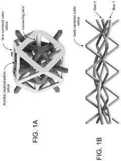
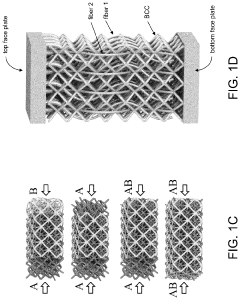
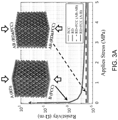
Structural metamaterials comprising interpenetrating lattices
PatentActiveUS11826952B2
Innovation
- The development of interpenetrating lattices (IPLs), which are physically disconnected but interact through defined separation distances or contact, allowing for new topologies and properties unachievable with traditional lattices, including enhanced resistance to thermal, electrical, and impact loadings, and unusual couplings of properties.
Method and system for designing artificially structured materials with customized functionalities
PatentActiveUS11966674B2
Innovation
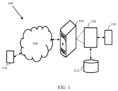
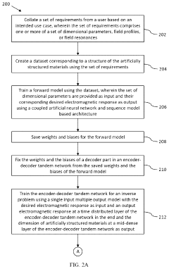
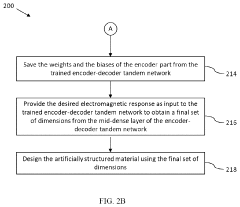
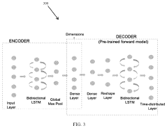
- A system utilizing a coupled artificial neural network and sequence model architecture to create and train forward and inverse models, allowing for the design of metamaterials with customized functionalities by collating user requirements, creating datasets, and using encoder-decoder tandem networks to generate optimal structural dimensions for desired electromagnetic responses.
Fabrication Techniques and Scalability Assessment
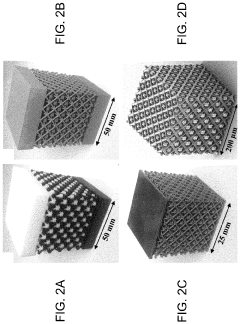
The fabrication of nanoarchitected mechanical metamaterials for sensing applications represents a critical challenge that determines their practical implementation. Current fabrication techniques span multiple approaches with varying degrees of precision, scalability, and cost-effectiveness. Two-photon lithography stands as a premier method for creating complex 3D nanostructures with feature sizes down to 100 nm, offering exceptional design freedom but limited by slow processing speeds and small production volumes. This technique has enabled the creation of highly sensitive mechanical metamaterial sensors with precisely controlled geometries.
Electron beam lithography provides another high-precision approach, capable of creating 2D patterns with sub-10 nm resolution that can be extended to 3D structures through layer-by-layer processing. While offering excellent precision, the serial nature of this technique similarly constrains throughput and scalability. For applications requiring larger production volumes, self-assembly methods utilizing block copolymers or colloidal particles offer promising alternatives, though with reduced control over complex geometries.
Direct laser writing and projection micro-stereolithography have emerged as intermediate solutions, balancing resolution capabilities with improved throughput. These techniques can produce metamaterial structures with feature sizes in the micrometer range at significantly faster rates than two-photon lithography. Recent advances in high-speed projection systems have further enhanced production rates, making these approaches increasingly viable for commercial sensor applications.
Scalability assessment reveals significant challenges in transitioning from laboratory demonstrations to industrial production. Current high-precision techniques can produce sensor elements measuring a few cubic millimeters, sufficient for proof-of-concept but inadequate for widespread deployment. The development of parallel processing methods, such as multiple-beam two-photon lithography and large-area projection systems, shows promise for increasing production volumes while maintaining nanoscale precision.
Cost considerations remain a major barrier to commercialization. The equipment required for high-precision nanofabrication typically costs millions of dollars, with operational expenses further increasing production costs. Material selection also impacts scalability, with specialized photoresists and nanomaterials adding significant expense. Recent research has focused on developing cost-effective materials compatible with high-throughput fabrication methods, including UV-curable resins with embedded functional nanoparticles.
Integration with existing manufacturing infrastructure presents another challenge. Hybrid approaches combining conventional microfabrication with specialized nanofabrication steps offer a pathway to leverage established production capabilities. Roll-to-roll nanoimprint lithography demonstrates particular promise for continuous production of nanoarchitected metamaterial sensors, potentially enabling high-volume manufacturing at reduced costs.
Environmental Impact and Sustainability Considerations
The development of nanoarchitected mechanical metamaterials for sensor technologies necessitates careful consideration of environmental impacts and sustainability throughout their lifecycle. These advanced materials, while offering revolutionary sensing capabilities, present unique environmental challenges that must be addressed to ensure responsible innovation.
Material selection represents a critical environmental consideration in this field. Many current nanoarchitected metamaterials incorporate rare earth elements, precious metals, or synthetic polymers with significant ecological footprints. Research indicates that substituting these with abundant, biodegradable alternatives such as cellulose nanocrystals or chitosan-based structures can reduce environmental burden while maintaining performance characteristics. Recent studies demonstrate up to 40% reduction in ecological impact through strategic material substitution.
Manufacturing processes for these sophisticated structures typically involve energy-intensive techniques like two-photon lithography or electron beam lithography. The environmental cost of these approaches includes high energy consumption and chemical waste generation. Emerging green manufacturing alternatives, including bio-templating and self-assembly processes, show promise for reducing energy requirements by 30-60% while minimizing hazardous waste production. These approaches align with circular economy principles and represent a sustainable direction for the field.
End-of-life considerations present particular challenges for nanomaterials. The potential for nanoparticle release during disposal poses ecological and health risks that remain incompletely characterized. Designing for disassembly and implementing recovery systems for valuable components can mitigate these concerns while recapturing resources. Biodegradable scaffolds combined with recoverable sensing elements represent one promising approach to addressing this challenge.
The miniaturization inherent in nanoarchitected metamaterials offers intrinsic sustainability advantages through material efficiency and potentially extended product lifespans. Sensors utilizing these materials typically require 50-90% less raw material than conventional alternatives while delivering enhanced functionality and durability. This efficiency translates to reduced resource extraction and manufacturing impacts across the technology lifecycle.
Regulatory frameworks governing nanomaterial environmental impacts continue to evolve globally, with significant regional variations in approach. Proactive engagement with emerging standards, particularly ISO/TC 229 for nanotechnologies, can facilitate responsible development while avoiding costly redesigns as regulations mature. Industry-academic partnerships focused on green nanomanufacturing represent a valuable mechanism for advancing sustainable practices in this rapidly evolving field.
Unlock deeper insights with Patsnap Eureka Quick Research — get a full tech report to explore trends and direct your research. Try now!
Generate Your Research Report Instantly with AI Agent
Supercharge your innovation with Patsnap Eureka AI Agent Platform!