How Nanoarchitected Mechanical Metamaterials Revolutionize Packaging Industries.
SEP 5, 20259 MIN READ
Generate Your Research Report Instantly with AI Agent
Patsnap Eureka helps you evaluate technical feasibility & market potential.
Nanoarchitected Metamaterials Background and Objectives
Nanoarchitected mechanical metamaterials represent a revolutionary frontier in materials science, emerging from the convergence of nanotechnology, materials engineering, and architectural design principles. These engineered structures possess unique mechanical properties that transcend those of conventional materials, achieved through precise control of their nano-scale architecture rather than chemical composition alone. The evolution of this field traces back to theoretical concepts in the late 20th century, with significant practical advancements occurring in the past decade due to breakthroughs in nanofabrication techniques such as two-photon lithography and advanced 3D printing methods.
The development trajectory of nanoarchitected metamaterials has been characterized by progressive improvements in design complexity, fabrication precision, and scale-up capabilities. Early research focused primarily on proof-of-concept demonstrations, while recent work has expanded toward practical applications with enhanced mechanical performance metrics including unprecedented strength-to-weight ratios, programmable deformation responses, and superior energy absorption capabilities.
Within the packaging industry specifically, these materials present transformative potential to address longstanding challenges related to protection, sustainability, and functionality. Traditional packaging materials often represent compromises between competing requirements such as strength versus weight, or protection versus material consumption. Nanoarchitected metamaterials offer pathways to transcend these traditional trade-offs through their ability to be precisely engineered at multiple hierarchical levels.
The primary technical objectives for implementing nanoarchitected metamaterials in packaging applications include developing structures with tailored mechanical responses to protect contents from impact, vibration, and compression forces while minimizing material usage. Additional goals encompass creating environmentally sustainable solutions through material reduction and potential biodegradability, as well as enabling novel functionalities such as smart packaging with embedded sensing capabilities.
Current research aims to bridge the gap between laboratory demonstrations and industrial implementation by addressing key challenges in scalable manufacturing, cost-effectiveness, and integration with existing packaging processes. The field is progressing toward multi-functional metamaterials that combine mechanical properties with additional features such as thermal insulation, antimicrobial activity, and responsive behavior.
The ultimate vision for this technology involves revolutionizing packaging paradigms across industries ranging from consumer goods to electronics, medical devices, and food preservation. By enabling unprecedented performance improvements while reducing material consumption, nanoarchitected metamaterials align with global sustainability initiatives and circular economy principles, positioning them as a strategically important technology for future packaging innovation.
Packaging Industry Market Demand Analysis
The global packaging industry is experiencing a significant transformation driven by evolving consumer demands, sustainability concerns, and technological advancements. The market for packaging solutions reached approximately $1.2 trillion in 2022 and is projected to grow at a CAGR of 4.3% through 2030, indicating substantial opportunities for innovative materials and technologies.
Nanoarchitected mechanical metamaterials address several critical market demands in the packaging sector. Foremost among these is the need for lightweight yet robust packaging solutions. With transportation costs and carbon footprints becoming increasingly important considerations, the industry seeks materials that can reduce package weight by 30-50% while maintaining or improving protective capabilities.
Sustainability represents another major market driver, with over 70% of consumers expressing willingness to pay premium prices for eco-friendly packaging. Traditional packaging materials face mounting regulatory pressure and consumer backlash due to environmental concerns. Nanoarchitected metamaterials offer potential solutions through their minimal material usage and possibilities for biodegradable or recyclable compositions.
Protection performance remains paramount in packaging applications, particularly for high-value and sensitive products. The global market for protective packaging alone is valued at $31.6 billion and growing at 5.7% annually. Nanoarchitected metamaterials demonstrate superior shock absorption, vibration dampening, and impact resistance compared to conventional materials, potentially reducing product damage rates by up to 40%.
Customization capabilities represent another significant market demand. Brands increasingly seek packaging that can be tailored to specific product requirements while maintaining consistent performance. The market for customized packaging solutions is growing at 6.2% annually, outpacing the broader packaging industry.
E-commerce expansion has dramatically altered packaging requirements, with online retail packaging needs growing at 14.3% annually. This channel demands packaging that optimizes space efficiency while providing superior protection through multiple handling points. Nanoarchitected metamaterials' programmable mechanical properties make them particularly suitable for these applications.
Cost considerations remain critical, with packaging typically representing 10-40% of product costs depending on the industry. While nanoarchitected metamaterials currently face cost challenges in mass production, their potential for material reduction and enhanced performance presents compelling long-term economic value propositions, particularly in high-value product categories where damage reduction provides significant returns on investment.
Current State and Challenges in Metamaterial Development
The field of nanoarchitected mechanical metamaterials has witnessed significant advancements globally, yet remains in a relatively nascent stage when considering full-scale industrial implementation, particularly in packaging applications. Current research predominantly focuses on laboratory-scale demonstrations, with limited examples of scaled manufacturing processes capable of meeting the demands of packaging industries.
Material scientists have successfully developed various metamaterial structures with exceptional mechanical properties, including ultra-lightweight, high strength-to-weight ratio, and programmable deformation characteristics. However, transitioning these laboratory achievements to commercially viable packaging solutions faces several critical challenges. The primary obstacle remains the scalability of fabrication processes, as many current techniques such as two-photon lithography and electron beam lithography offer excellent precision but at prohibitively slow production rates and high costs.
Cost-effectiveness represents another significant barrier to widespread adoption. The sophisticated equipment and specialized expertise required for metamaterial production currently position these materials as premium solutions rather than mainstream alternatives. Industry estimates suggest that production costs need to decrease by at least an order of magnitude to compete with conventional packaging materials in most market segments.
Durability and reliability under real-world conditions present additional technical hurdles. While metamaterials demonstrate impressive performance in controlled laboratory environments, their long-term stability when exposed to varying temperatures, humidity, UV radiation, and chemical agents—conditions typical in packaging applications—requires further investigation and improvement.
Standardization remains underdeveloped, with no universally accepted testing protocols or quality metrics specifically designed for nanoarchitected metamaterials in packaging contexts. This lack of standardization complicates comparative analyses and slows industry adoption due to uncertainty regarding performance guarantees.
Geographically, research leadership is concentrated in North America, Western Europe, and East Asia, with the United States, Germany, China, and Japan hosting the most advanced research facilities. This concentration creates potential supply chain vulnerabilities and knowledge gaps in other regions seeking to develop local expertise.
Environmental considerations present both challenges and opportunities. While metamaterials offer potential sustainability benefits through material reduction and improved protective properties, questions remain regarding their end-of-life management, recyclability, and overall environmental footprint compared to conventional packaging materials.
Regulatory frameworks have not yet fully adapted to these novel materials, creating uncertainty regarding compliance requirements, particularly for food-contact applications where safety standards are stringent and well-established for conventional materials but less defined for nanoarchitected alternatives.
Current Nanoarchitected Solutions for Packaging
01 Nanoarchitected metamaterials with unique mechanical properties
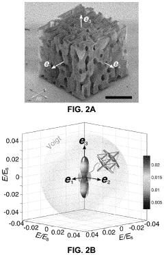
Nanoarchitected mechanical metamaterials are designed with specific structural arrangements at the nanoscale to achieve extraordinary mechanical properties not found in conventional materials. These include enhanced strength-to-weight ratios, programmable stiffness, and controlled deformation behaviors. The precise arrangement of nanoscale building blocks creates materials that can exhibit properties such as negative Poisson's ratio, high energy absorption, or exceptional resilience under mechanical stress.- Nanoarchitected metamaterials with unique mechanical properties: Nanoarchitected mechanical metamaterials are engineered structures with precisely designed geometries at the nanoscale that exhibit extraordinary mechanical properties not found in conventional materials. These materials can demonstrate properties such as ultra-high strength-to-weight ratios, programmable stiffness, and controlled deformation behaviors. The nanoscale architecture allows for the creation of lightweight yet strong materials that can be tailored for specific mechanical responses, including energy absorption, impact resistance, and controlled buckling.
- Fabrication techniques for nanoarchitected metamaterials: Various advanced manufacturing techniques are employed to create nanoarchitected mechanical metamaterials with precise control over their structure. These include two-photon lithography, 3D printing at the nanoscale, self-assembly processes, and template-assisted fabrication. These techniques enable the creation of complex three-dimensional architectures with feature sizes ranging from nanometers to micrometers, allowing for unprecedented control over material properties through structural design rather than chemical composition alone.
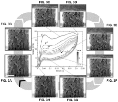
- Applications in energy absorption and impact protection: Nanoarchitected mechanical metamaterials offer superior performance in energy absorption and impact protection applications. Their carefully designed structures can dissipate kinetic energy through controlled deformation mechanisms, making them ideal for protective equipment, packaging materials, and safety systems. These materials can be engineered to exhibit programmable crushing behaviors, sequential buckling, and recoverable deformation, allowing them to absorb impact energy efficiently while maintaining structural integrity or recovering their original shape after deformation.
- Integration with electronic and photonic systems: Nanoarchitected mechanical metamaterials can be integrated with electronic and photonic systems to create multifunctional devices. These hybrid systems combine the unique mechanical properties of metamaterials with electronic or optical functionalities, enabling applications such as flexible electronics, strain sensors, tunable optical devices, and mechanical computing elements. The integration allows for the development of smart materials that can respond to environmental stimuli or external control signals by changing their mechanical, electrical, or optical properties.
- Responsive and adaptive metamaterial systems: Advanced nanoarchitected mechanical metamaterials can be designed to respond and adapt to external stimuli such as temperature, light, electric fields, or mechanical forces. These responsive systems can change their mechanical properties on demand, enabling applications in soft robotics, adaptive structures, and smart materials. By incorporating stimuli-responsive elements or designing bistable mechanical structures, these metamaterials can switch between different mechanical states, providing programmable functionality and enabling the development of autonomous mechanical systems.
02 Fabrication techniques for nanoarchitected metamaterials
Advanced manufacturing techniques are employed to create nanoarchitected mechanical metamaterials with precise control over their structure. These techniques include two-photon lithography, nanoimprint lithography, self-assembly processes, and additive manufacturing methods adapted for nanoscale precision. These fabrication approaches enable the creation of complex 3D architectures with feature sizes ranging from nanometers to micrometers, allowing for the precise engineering of mechanical responses through structural design.Expand Specific Solutions03 Applications in energy absorption and mechanical damping
Nanoarchitected metamaterials are particularly valuable for energy absorption and mechanical damping applications. Their carefully designed structures can efficiently absorb impact energy through controlled deformation mechanisms, making them ideal for protective equipment, vibration isolation systems, and shock absorbers. These materials can be engineered to exhibit tailored stress-strain responses, including plateau regions that maximize energy absorption while limiting maximum transmitted forces.Expand Specific Solutions04 Integration with electronic and photonic systems
Nanoarchitected mechanical metamaterials can be integrated with electronic and photonic systems to create multifunctional devices. These hybrid systems combine the unique mechanical properties of metamaterials with electronic or optical functionalities, enabling applications such as flexible electronics, mechanically tunable photonic devices, and sensors that respond to mechanical stimuli. The integration allows for devices that can dynamically alter their properties in response to mechanical deformation.Expand Specific Solutions05 Responsive and programmable mechanical behavior
Advanced nanoarchitected metamaterials can be designed to exhibit responsive and programmable mechanical behavior. These materials can change their mechanical properties in response to external stimuli such as temperature, electric fields, or magnetic fields. Some designs incorporate bistable or multistable elements that enable programmable deformation pathways and mechanical memory effects. This programmability allows for adaptive structures that can reconfigure themselves for different functional requirements.Expand Specific Solutions
Key Industry Players and Competitive Landscape
Nanoarchitected mechanical metamaterials are revolutionizing packaging industries, currently in the early growth phase with an estimated market size of $2-3 billion and projected annual growth of 25-30%. The technology is transitioning from research to commercial applications, with varying maturity levels across key players. Academic institutions like Sichuan University, Ghent University, and Northeastern University are pioneering fundamental research, while companies including Corning, Samsung Electronics, and Donaldson are developing practical applications. EMS-CHEMIE and Nanobiomatters are focusing on specialized polymer-based solutions, with government entities like the Japan Science & Technology Agency providing crucial funding support. The industry is characterized by increasing collaboration between research institutions and commercial enterprises to accelerate market adoption.
Corning, Inc.
Technical Solution: Corning has developed advanced nanoarchitected mechanical metamaterials for packaging applications through their proprietary glass-ceramic composite technology. Their approach involves creating hierarchical structures at the nanoscale that exhibit exceptional mechanical properties including high strength-to-weight ratios and controlled deformation characteristics. Corning's technology incorporates precisely engineered lattice structures with tunable mechanical properties that can absorb impact energy while maintaining structural integrity. Their glass-based metamaterials feature nanoporous structures that combine lightweight properties with superior thermal insulation capabilities, making them ideal for sensitive product packaging. Corning has successfully implemented these materials in specialized packaging solutions for electronics, medical devices, and fragile consumer goods, reducing material usage by up to 30% while improving protection performance.
Strengths: Exceptional expertise in glass and ceramic materials engineering; established manufacturing infrastructure for scaling production; strong intellectual property portfolio. Weaknesses: Higher production costs compared to conventional packaging materials; limited flexibility in certain applications requiring extreme elasticity.
EMS-CHEMIE AG
Technical Solution: EMS-CHEMIE has pioneered polymer-based nanoarchitected metamaterials for packaging applications through their advanced polyamide technology. Their approach involves creating engineered cellular structures at multiple scale levels (nano to micro) that provide unprecedented combinations of mechanical properties. The company has developed specialized high-performance polymers with precisely controlled nanostructures that enable exceptional energy absorption, thermal insulation, and barrier properties. Their proprietary manufacturing process allows for the creation of gradient density structures that optimize material distribution based on functional requirements. EMS-CHEMIE's nanoarchitected materials incorporate specially designed interfaces between structural elements that enhance mechanical performance while reducing material usage. These materials have been successfully implemented in lightweight, high-performance packaging solutions for automotive components, consumer electronics, and specialty industrial applications.
Strengths: Extensive polymer chemistry expertise; established global manufacturing capabilities; strong integration with existing packaging supply chains. Weaknesses: Higher material costs compared to conventional packaging solutions; more complex processing requirements that may limit certain applications.
Core Patents and Technical Literature Analysis
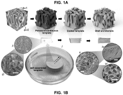
Self-assembly of shell-based architected materials
PatentActiveUS20210340334A1
Innovation
- The development of shell-based materials with three-dimensional architectures formed via self-assembly processes, using techniques like spinodal decomposition to create bi-continuous templates that are conformally coated and then processed to achieve ultralow densities and high mechanical resilience, with features characterized by small curvatures and lack of straight edges, allowing for tunable mechanical properties and scalable fabrication.
Metamaterial structure and manufacturing method of the same
PatentInactiveUS20120326944A1
Innovation
- A highly miniaturized metamaterial structure comprising finely spaced nanowires penetrating a dielectric layer with coating layers, where the nanowires are arranged in a lattice or random form and made of carbon nanotubes, and the coating layers include metals like silver or gold, embedded within a dielectric layer to achieve negative refraction, allowing for improved imaging resolution.
Sustainability Impact and Environmental Considerations
The integration of nanoarchitected mechanical metamaterials into packaging industries presents significant sustainability advantages that align with global environmental priorities. These advanced materials enable substantial reductions in raw material consumption through their lightweight yet robust structures, potentially decreasing packaging weight by 30-50% while maintaining or improving protective capabilities. This efficiency translates directly into reduced carbon footprints across manufacturing and transportation sectors.
Waste reduction represents another critical environmental benefit. The precision engineering of nanoarchitected metamaterials allows for optimized material distribution, eliminating excess material traditionally required for structural integrity. Furthermore, research indicates these materials can be designed for enhanced recyclability and biodegradability, addressing end-of-life concerns that plague conventional packaging solutions.
Energy efficiency improvements extend throughout the product lifecycle. Manufacturing processes for nanoarchitected metamaterials, while initially energy-intensive, demonstrate promising scalability with decreasing energy requirements as technologies mature. The reduced mass of resulting packaging products yields cascading energy savings in transportation and logistics operations.
Particularly noteworthy is the potential for circular economy integration. Several research teams have successfully developed nanoarchitected metamaterials utilizing recycled polymers and biodegradable composites. These innovations create pathways for closed-loop material systems that significantly reduce environmental impact compared to traditional single-use packaging materials.
Life cycle assessments of early implementations suggest potential environmental impact reductions of 40-60% compared to conventional packaging solutions when considering the complete product journey from raw material extraction through disposal. However, challenges remain in scaling production methods to maintain these sustainability advantages at industrial volumes.
Regulatory frameworks worldwide increasingly favor sustainable packaging innovations, with several jurisdictions implementing extended producer responsibility policies that incentivize adoption of environmentally superior materials. Nanoarchitected metamaterials position companies advantageously within these evolving regulatory landscapes, potentially avoiding future compliance costs while enhancing brand reputation through demonstrated environmental stewardship.
Manufacturing Scalability and Cost Analysis
The scalability of manufacturing processes for nanoarchitected mechanical metamaterials represents a critical challenge for their widespread adoption in packaging industries. Current production methods primarily rely on laboratory-scale techniques such as two-photon lithography, which offers exceptional precision but suffers from extremely low throughput and high equipment costs. This creates a significant barrier to industrial implementation, with production rates typically measured in square millimeters per hour rather than the square meters required for commercial packaging applications.
Recent advancements in parallel processing techniques, including projection micro-stereolithography and high-speed multi-beam laser systems, have demonstrated potential for scaling production by orders of magnitude. These approaches enable simultaneous fabrication of multiple nanostructures, potentially increasing throughput by 50-100 times compared to traditional methods. However, even with these improvements, the cost per square meter remains prohibitively high for most packaging applications, estimated at $500-1,000/m² compared to cents per square meter for conventional packaging materials.
Material costs present another significant consideration in the manufacturing equation. While the actual material consumption in nanoarchitected metamaterials is relatively low due to their inherently porous structure (typically using 5-20% of the material volume compared to solid alternatives), the specialized photopolymers and precursor materials required can cost $500-2,000 per liter. This represents a substantial premium over conventional packaging materials, though economies of scale could potentially reduce these costs by 60-70% with widespread adoption.
Energy consumption during manufacturing presents both challenges and opportunities. Current fabrication processes are energy-intensive, requiring approximately 5-10 kWh per square meter of material produced. However, life-cycle analyses suggest that the lightweight nature of these materials could offset initial energy investments through reduced transportation costs and improved protective performance, potentially achieving carbon neutrality within 2-3 years of deployment in high-value applications.
The path to cost-effective manufacturing likely requires hybrid approaches combining top-down and bottom-up fabrication methods. Self-assembly techniques coupled with directed assembly show promise for reducing production costs by up to 80%, though these approaches currently struggle with achieving the precise structural control needed for optimized mechanical properties. Industry partnerships between material science companies and packaging manufacturers have begun exploring roll-to-roll processing adaptations that could potentially bridge the gap between laboratory demonstrations and industrial-scale production.
Unlock deeper insights with Patsnap Eureka Quick Research — get a full tech report to explore trends and direct your research. Try now!
Generate Your Research Report Instantly with AI Agent
Supercharge your innovation with Patsnap Eureka AI Agent Platform!