Back-End-Of-Line Compatibility For PMA MRAM Integration
AUG 22, 20259 MIN READ
Generate Your Research Report Instantly with AI Agent
Patsnap Eureka helps you evaluate technical feasibility & market potential.
PMA MRAM Integration Background and Objectives
Perpendicular Magnetic Anisotropy Magnetoresistive Random Access Memory (PMA MRAM) has emerged as a promising non-volatile memory technology over the past decade. The evolution of MRAM technology began with in-plane magnetic anisotropy devices, which faced significant challenges in terms of scalability and power consumption. The transition to PMA-based structures marked a critical advancement, enabling higher thermal stability, reduced switching current, and improved scalability for sub-45nm technology nodes.
The fundamental principle of PMA MRAM relies on the perpendicular orientation of magnetic moments relative to the film plane, which offers superior magnetic properties compared to its in-plane counterparts. This configuration allows for more efficient spin-transfer torque (STT) or spin-orbit torque (SOT) switching mechanisms, which are essential for reliable write operations in high-density memory applications.
The integration of PMA MRAM into existing semiconductor manufacturing processes presents unique challenges, particularly regarding Back-End-Of-Line (BEOL) compatibility. BEOL processes typically involve temperatures below 400°C to preserve the integrity of metal interconnects and low-k dielectrics. However, conventional PMA materials often require high-temperature annealing (>400°C) to achieve the desired magnetic properties, creating a fundamental conflict with BEOL thermal budgets.
The technical objectives for PMA MRAM integration focus on developing materials and processes that maintain excellent magnetic properties while remaining compatible with standard BEOL thermal constraints. This includes exploring novel material stacks that can establish robust perpendicular magnetic anisotropy at lower processing temperatures, as well as innovative deposition and annealing techniques that minimize thermal exposure of surrounding structures.
Another critical objective is to ensure the scalability of PMA MRAM technology to sub-20nm dimensions without compromising performance metrics such as thermal stability factor (Δ), tunnel magnetoresistance ratio (TMR), and switching current density. This requires precise engineering of the magnetic tunnel junction (MTJ) structure, including the free layer, reference layer, and tunnel barrier.
Additionally, the integration must address reliability concerns such as read disturb immunity, write endurance, and data retention at elevated operating temperatures. These parameters are particularly important for automotive and industrial applications where extended temperature ranges are common requirements.
The ultimate goal of PMA MRAM BEOL integration research is to establish a manufacturing-ready technology that combines the non-volatility, high endurance, and fast switching speed of MRAM with seamless compatibility with standard CMOS fabrication flows. This would position PMA MRAM as a viable universal memory solution capable of replacing multiple memory types in future computing architectures, from embedded cache to storage class memory applications.
Market Analysis for BEOL-Compatible MRAM Solutions
The MRAM market is experiencing significant growth, with projections indicating a compound annual growth rate (CAGR) of 29.7% from 2021 to 2026, potentially reaching a market value of $1.6 billion by 2026. This growth is primarily driven by increasing demand for non-volatile memory solutions that combine the speed of SRAM, the density of DRAM, and the non-volatility of flash memory.
BEOL-compatible MRAM solutions specifically address a critical market need for memory technologies that can be integrated into existing semiconductor manufacturing processes without requiring significant modifications to front-end processes. This compatibility significantly reduces implementation costs and accelerates time-to-market for semiconductor manufacturers looking to incorporate MRAM technology.
The automotive sector represents one of the most promising markets for BEOL-compatible MRAM, particularly for advanced driver-assistance systems (ADAS) and autonomous vehicles, which require reliable, high-speed, non-volatile memory that can operate in extreme temperature conditions. The industrial IoT sector also shows substantial demand potential, with applications in smart manufacturing, where MRAM's radiation hardness and reliability provide significant advantages.
Consumer electronics manufacturers are increasingly interested in MRAM for mobile devices, where its low power consumption can extend battery life while providing instant-on capabilities. The enterprise storage market is another significant segment, with data centers seeking energy-efficient, high-performance memory solutions to handle growing data processing demands.
Geographically, North America currently leads the MRAM market, followed by Asia-Pacific and Europe. However, the Asia-Pacific region is expected to show the highest growth rate due to the concentration of semiconductor manufacturing facilities and increasing adoption of advanced electronics in countries like China, South Korea, and Taiwan.
Market barriers for BEOL-compatible MRAM include competition from other emerging memory technologies such as ReRAM and PCRAM, as well as the established infrastructure supporting conventional memory technologies. Additionally, the relatively higher cost per bit compared to DRAM and flash memory remains a challenge, though this gap is expected to narrow as manufacturing processes mature and economies of scale are achieved.
Customer requirements are increasingly focused on reliability, endurance, and thermal stability, particularly for automotive and industrial applications. Data retention at higher temperatures is becoming a critical specification as MRAM expands into these markets. The ability to scale below 28nm while maintaining magnetic thermal stability represents both a significant market opportunity and a technical challenge for PMA MRAM integration.
BEOL Compatibility Challenges for PMA MRAM
The integration of Perpendicular Magnetic Anisotropy (PMA) Magnetic Random Access Memory (MRAM) into existing semiconductor fabrication processes presents significant Back-End-Of-Line (BEOL) compatibility challenges. These challenges stem primarily from the fundamental differences between conventional CMOS processing and the specialized requirements for magnetic materials and structures in MRAM devices.
Temperature constraints represent one of the most critical BEOL compatibility issues. While standard BEOL processes can withstand temperatures up to 400-450°C, magnetic tunnel junction (MTJ) stacks in PMA MRAM are extremely sensitive to thermal budgets. Temperatures exceeding 350°C can cause interdiffusion between layers, crystallization changes, and degradation of the CoFeB/MgO interface, resulting in compromised magnetic properties and reduced tunnel magnetoresistance (TMR) ratios.
Material contamination poses another significant challenge. Magnetic materials such as Co, Fe, and B are considered contaminants in conventional CMOS fabrication environments. Their introduction requires dedicated equipment and strict protocols to prevent cross-contamination that could affect device performance and reliability. The integration of these materials necessitates careful consideration of equipment segregation and process flow design.
Etching processes for MTJ stacks present unique difficulties compared to traditional CMOS materials. The multi-layer structure of MTJs, typically comprising 10-15 thin layers of different materials, requires highly selective and precisely controlled etching techniques. Physical etching methods often lead to redeposition issues and sidewall damage, while chemical etching lacks the selectivity needed for the diverse materials in the stack.
Structural integrity challenges arise from the mechanical stresses introduced during BEOL processing. Subsequent dielectric deposition, chemical-mechanical planarization (CMP), and metallization steps can induce mechanical stresses that affect the magnetic properties of the MTJ elements. These stresses may alter magnetic anisotropy or create defects at critical interfaces.
Scaling and dimensional control present additional hurdles as PMA MRAM moves toward advanced technology nodes. As MTJ dimensions shrink below 30nm, maintaining precise control over critical dimensions becomes increasingly difficult, affecting device uniformity and performance consistency across the wafer.
Electrical integration challenges include managing parasitic capacitances and resistances that can impact the sensing margin and switching performance of MRAM cells. The interface between the MTJ and surrounding BEOL structures must be carefully engineered to ensure reliable electrical connections while maintaining magnetic performance.
These BEOL compatibility challenges collectively represent a complex integration problem that requires innovative solutions spanning materials science, process engineering, and device physics to enable successful incorporation of PMA MRAM into mainstream semiconductor manufacturing processes.
Current BEOL Integration Approaches for PMA MRAM
01 PMA MRAM structure and fabrication for BEOL compatibility
Perpendicular Magnetic Anisotropy MRAM structures are designed with specific layer configurations to ensure compatibility with Back-End-Of-Line processes. These structures include specialized magnetic tunnel junctions (MTJs) with perpendicular magnetic anisotropy that can withstand the thermal budget of BEOL processing. The fabrication methods incorporate temperature-resistant materials and process steps that align with standard semiconductor manufacturing flows, enabling integration with CMOS technology without compromising device performance.- BEOL-compatible PMA MRAM fabrication techniques: Various fabrication techniques have been developed to ensure PMA MRAM compatibility with back-end-of-line (BEOL) processes. These include specialized deposition methods, thermal budget management, and integration schemes that protect the magnetic tunnel junction (MTJ) structures during subsequent processing steps. These techniques enable the integration of PMA MRAM into standard CMOS manufacturing flows without compromising the performance or reliability of either the memory elements or surrounding circuitry.
- Materials selection for BEOL-compatible PMA MRAM: Specific materials are selected for PMA MRAM structures to ensure compatibility with BEOL thermal budgets and processing conditions. These include carefully engineered magnetic layers with perpendicular magnetic anisotropy that can withstand BEOL processing temperatures, specialized barrier materials, and capping layers that protect the magnetic properties during integration. The selection of these materials is critical for maintaining the magnetic properties and performance of the MRAM devices throughout the manufacturing process.
- Thermal stability enhancements for BEOL processing: Various approaches have been developed to enhance the thermal stability of PMA MRAM structures during BEOL processing. These include specialized annealing techniques, thermal barrier layers, and material compositions that maintain perpendicular magnetic anisotropy at elevated temperatures. These enhancements ensure that the magnetic properties of the MRAM cells remain stable throughout the thermal cycles encountered during BEOL processing, preserving data retention capabilities and switching characteristics.
- Integration schemes for PMA MRAM in BEOL processes: Specific integration schemes have been developed for incorporating PMA MRAM into standard BEOL processes. These include specialized etch processes, planarization techniques, and interconnect strategies that enable the connection of MRAM cells to the underlying CMOS circuitry while maintaining compatibility with subsequent metallization layers. These integration approaches address challenges such as topography management, metal contamination prevention, and ensuring reliable electrical connections to the memory array.
- Circuit design considerations for BEOL PMA MRAM: Circuit design techniques have been developed to optimize the performance of PMA MRAM integrated in BEOL processes. These include specialized sense amplifiers, write drivers, and reference schemes that accommodate the electrical characteristics of PMA MRAM cells. Additionally, circuit designs address challenges related to process variations, thermal effects, and reliability concerns specific to BEOL-integrated magnetic memory. These circuit innovations enable robust operation of PMA MRAM arrays within the constraints of BEOL integration.
02 Thermal stability enhancements for BEOL processing
Thermal stability is critical for PMA MRAM devices to maintain their magnetic properties during high-temperature BEOL processes. Various approaches are employed to enhance thermal stability, including the use of specialized capping layers, heat-resistant magnetic materials, and thermal annealing techniques. These enhancements ensure that the magnetic properties of the MRAM cells remain stable throughout the manufacturing process and during device operation, even after exposure to elevated temperatures during BEOL processing.Expand Specific Solutions03 Integration techniques for PMA MRAM in semiconductor manufacturing
Specific integration techniques are developed to incorporate PMA MRAM into standard semiconductor manufacturing flows. These techniques include specialized etching processes, material deposition methods, and interconnect strategies that ensure proper electrical connections while maintaining BEOL compatibility. The integration approaches focus on minimizing process-induced damage to the magnetic layers and optimizing the interface between the MRAM cells and surrounding circuitry, enabling seamless incorporation into complex semiconductor devices.Expand Specific Solutions04 Low-temperature fabrication methods for BEOL compatibility
Low-temperature fabrication methods are developed specifically for PMA MRAM to ensure compatibility with BEOL thermal budgets. These methods include modified deposition techniques, alternative material systems, and specialized annealing processes that can be performed at reduced temperatures. By keeping processing temperatures within acceptable limits for BEOL integration, these approaches prevent damage to existing circuit elements while still achieving the desired magnetic properties for reliable MRAM operation.Expand Specific Solutions05 Materials engineering for BEOL-compatible PMA MRAM
Advanced materials engineering solutions are employed to create PMA MRAM structures that can withstand BEOL processing conditions. These include the development of specialized magnetic materials with high thermal stability, interface engineering to enhance perpendicular magnetic anisotropy, and barrier layers that prevent diffusion during high-temperature steps. The materials are carefully selected and engineered to maintain their functional properties throughout the manufacturing process, ensuring reliable device performance while remaining compatible with standard semiconductor fabrication flows.Expand Specific Solutions
Leading Companies in PMA MRAM Development
The Back-End-Of-Line (BEOL) compatibility for PMA MRAM integration market is currently in a growth phase, with increasing adoption across semiconductor manufacturing. The global MRAM market is projected to expand significantly as demand for non-volatile memory solutions rises in data centers, automotive, and IoT applications. Technologically, major players have achieved varying degrees of maturity in BEOL MRAM integration. IBM and Samsung lead with advanced manufacturing processes, while Everspin Technologies has established itself as a specialized MRAM provider. TSMC, GlobalFoundries, and SK Hynix are developing competitive solutions, with Qualcomm and Infineon focusing on application-specific implementations. Chinese companies like Huawei and Shanghai Huali are investing heavily to close the technological gap with established Western and Asian counterparts.
International Business Machines Corp.
Technical Solution: IBM has developed advanced BEOL (Back-End-Of-Line) compatible PMA (Perpendicular Magnetic Anisotropy) MRAM integration solutions that focus on thermal budget management and material stack optimization. Their approach includes using specialized CoFeB-MgO magnetic tunnel junctions with tuned thickness ratios (1.0-1.8nm) to maintain thermal stability during BEOL processing. IBM employs a unique "dual damascene" integration scheme that allows MRAM cells to be embedded between interconnect layers without compromising CMOS performance. Their process includes specialized capping layers and thermal annealing sequences (300-400°C) to preserve the magnetic properties while ensuring compatibility with standard semiconductor manufacturing flows. IBM has demonstrated successful integration of PMA MRAM with 14nm and 7nm technology nodes, achieving write endurance exceeding 10^12 cycles and data retention of over 10 years at 85°C.
Strengths: Industry-leading expertise in material science and process integration; extensive patent portfolio covering MRAM integration techniques; demonstrated production-ready solutions at advanced nodes. Weaknesses: Higher manufacturing complexity compared to conventional memory technologies; thermal budget constraints may limit some applications; integration costs remain higher than competing non-volatile memory solutions.
Taiwan Semiconductor Manufacturing Co., Ltd.
Technical Solution: TSMC has developed a comprehensive BEOL-compatible PMA MRAM integration platform that addresses the challenges of embedding magnetic materials within standard CMOS processes. Their approach centers on a "via-middle" integration scheme where the MRAM cell is positioned between specific metal layers (typically between M4 and M5) to optimize performance while minimizing process disruption. TSMC's solution includes specialized diffusion barriers using TaN/Ta multilayers to prevent metal contamination, and they've engineered precise thermal profiles for post-MTJ processing that maintain magnetic properties while staying within BEOL thermal constraints. Their integration methodology incorporates advanced CMP (Chemical Mechanical Polishing) techniques to ensure planarization compatibility with subsequent interconnect layers. TSMC has demonstrated successful integration of PMA MRAM in their 22nm, 16nm, and 7nm technology nodes, achieving switching currents below 50μA with TMR (Tunneling Magnetoresistance) ratios exceeding 200% and write endurance above 10^10 cycles.
Strengths: World-class manufacturing infrastructure; ability to integrate MRAM into various technology nodes; established ecosystem for customer adoption. Weaknesses: Higher implementation costs compared to conventional embedded memories; process complexity increases yield challenges; thermal budget limitations constrain some design options.
Key Patents and Innovations in BEOL-Compatible MRAM
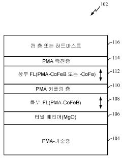
Thermally tolerant perpendicular magnetic anisotropy coupled elements for spin-transfer torque switching device
PatentWO2013044190A1
Innovation
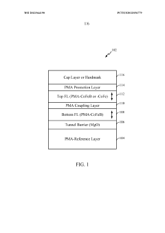
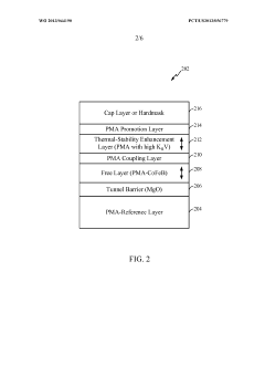
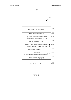
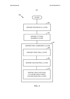
- A magnetic tunnel junction configuration is developed with a composite PMA layer and a PMA coupling layer, using a relatively thick CoFeB layer with an assist layer to enhance perpendicular magnetic anisotropy, thereby increasing thermal stability without increasing switching current density.
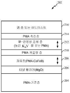
Thermally tolerant perpendicular magnetic anisotropy coupled elements for spin-transfer torque switching device
PatentInactiveKR1020170001739A
Innovation
- The implementation of a composite PMA layer with a thick CoFeB layer and an auxiliary layer, coupled by a PMA coupling layer, to provide perpendicular magnetic anisotropy, enhancing thermal stability and reducing switching current density without increasing the damping constant.
Thermal Budget Management Strategies
Thermal budget management represents a critical challenge in the integration of PMA (Perpendicular Magnetic Anisotropy) MRAM technology with standard CMOS processes. The primary concern stems from the high-temperature annealing steps required for CMOS fabrication, which can potentially degrade the magnetic properties of MRAM materials when introduced in the Back-End-Of-Line (BEOL) stages.
Industry standards typically limit BEOL processing temperatures to approximately 400°C to maintain interconnect integrity. However, PMA MRAM materials, particularly the MgO tunnel barrier and CoFeB magnetic layers, exhibit thermal sensitivity that necessitates careful thermal budget allocation. Experimental data indicates that exposure to temperatures exceeding 350-400°C for extended periods can trigger crystallization changes, interfacial diffusion, and magnetic property alterations that compromise device performance.
Several thermal budget management strategies have emerged to address these challenges. The implementation of low-temperature deposition techniques, such as atomic layer deposition (ALD) and low-temperature physical vapor deposition (PVD), has proven effective in minimizing thermal exposure during MRAM stack formation. These approaches typically operate below 300°C while maintaining film quality and interface characteristics essential for TMR (Tunneling Magnetoresistance) performance.
Material engineering represents another crucial strategy, with researchers developing thermally robust magnetic materials through composition optimization. The incorporation of thermal diffusion barriers, typically utilizing Ta, Ru, or W layers, has demonstrated significant improvements in preventing interdiffusion between magnetic layers during thermal processing. Additionally, the introduction of thermal stabilizers like Hf, Mo, or W into CoFeB layers has enhanced their crystallization temperature thresholds by 50-75°C in recent studies.
Process sequence optimization has emerged as a complementary approach, where MRAM integration occurs after high-temperature CMOS processing steps. This "MRAM-last" integration scheme minimizes exposure to thermal cycles, though it introduces additional lithography alignment challenges. Some manufacturers have implemented rapid thermal annealing (RTA) with precisely controlled temperature ramps and durations to achieve necessary crystallization while minimizing thermal exposure time.
Advanced cooling strategies during deposition and post-processing have also gained traction. These include substrate cooling during sputter deposition and the implementation of heat-sink layers within the stack architecture. Computational thermal modeling has become increasingly important, enabling process engineers to simulate thermal profiles throughout the fabrication sequence and identify potential hotspots or cumulative thermal exposure issues before physical implementation.
Materials Science Advancements for BEOL Compatibility
The development of materials science has been pivotal in addressing the thermal budget constraints associated with Back-End-Of-Line (BEOL) compatibility for Perpendicular Magnetic Anisotropy Magnetic Random Access Memory (PMA MRAM) integration. Traditional ferromagnetic materials used in MRAM devices often require high annealing temperatures (>400°C) that exceed BEOL thermal budgets, which typically restrict processing temperatures to below 400°C to prevent damage to underlying interconnect structures.
Recent advancements in materials engineering have focused on developing novel magnetic multilayer stacks that can achieve the required perpendicular magnetic anisotropy at lower processing temperatures. Specifically, CoFeB/MgO-based structures have emerged as promising candidates, with researchers successfully demonstrating PMA formation at temperatures as low as 300°C through careful control of layer thicknesses and compositions.
The incorporation of synthetic antiferromagnetic (SAF) structures has further enhanced BEOL compatibility by improving thermal stability while maintaining lower processing temperatures. These structures utilize Ru spacer layers between ferromagnetic layers to create strong antiferromagnetic coupling, resulting in enhanced magnetic properties without requiring high-temperature annealing steps.
Another significant advancement has been the development of seed and capping layers that promote crystallization and texture formation at reduced temperatures. Materials such as Ta, W, and Hf have shown promise as seed layers that facilitate the growth of high-quality magnetic films with strong PMA characteristics while remaining within BEOL thermal constraints.
Interface engineering has emerged as a critical aspect of materials science for BEOL-compatible MRAM. Researchers have demonstrated that carefully controlled oxidation at the CoFeB/MgO interface can significantly enhance PMA without requiring high-temperature annealing. This approach has enabled the achievement of sufficient magnetic performance while maintaining BEOL compatibility.
The exploration of alternative magnetic materials, including Heusler alloys and rare-earth transition metal alloys, represents another frontier in materials science for BEOL-compatible MRAM. These materials offer intrinsically higher magnetic anisotropy, potentially eliminating the need for high-temperature annealing altogether. Recent studies have shown promising results with Co-based Heusler alloys that exhibit PMA at processing temperatures below 350°C.
Atomic layer deposition (ALD) and other advanced deposition techniques have also contributed significantly to materials advancement for BEOL compatibility. These methods enable precise control over layer thicknesses and interfaces at the atomic scale, resulting in enhanced magnetic properties even at lower processing temperatures.
Unlock deeper insights with Patsnap Eureka Quick Research — get a full tech report to explore trends and direct your research. Try now!
Generate Your Research Report Instantly with AI Agent
Supercharge your innovation with Patsnap Eureka AI Agent Platform!