

Defect Tolerance And Yield Considerations For PMA MTJs
AUG 22, 20259 MIN READ
Generate Your Research Report Instantly with AI Agent
Patsnap Eureka helps you evaluate technical feasibility & market potential.
PMA MTJ Technology Background and Objectives
Perpendicular Magnetic Anisotropy Magnetic Tunnel Junctions (PMA MTJs) have emerged as a revolutionary technology in the field of non-volatile memory devices over the past decade. The evolution of this technology can be traced back to the discovery of the tunneling magnetoresistance (TMR) effect in the 1990s, which laid the foundation for magnetic random-access memory (MRAM) development. The transition from in-plane magnetic anisotropy to perpendicular magnetic anisotropy marked a significant milestone, enabling higher thermal stability and reduced switching current requirements.
The technological trajectory of PMA MTJs has been characterized by continuous improvements in materials science, particularly in the development of CoFeB/MgO interfaces that exhibit strong perpendicular anisotropy. This advancement has been crucial for scaling devices to smaller dimensions while maintaining thermal stability, a prerequisite for high-density memory applications. Recent years have witnessed the integration of spin-orbit torque (SOT) mechanisms, further enhancing switching efficiency and reliability.
The primary technical objectives in PMA MTJ development center around addressing defect tolerance and yield considerations, which have become increasingly critical as device dimensions shrink below 30nm. These objectives include: enhancing manufacturing yield through improved material deposition techniques; developing robust defect detection methodologies; implementing error correction strategies at both device and system levels; and establishing predictive models for defect formation and propagation during fabrication processes.
Current research aims to achieve defect densities below 0.1 defects/cm² while maintaining TMR ratios exceeding 200% and thermal stability factors above 60 at sub-20nm dimensions. These parameters are essential for ensuring reliable operation in commercial applications with data retention periods of 10+ years. Additionally, there is a focused effort to develop fabrication processes that can tolerate certain types of defects without compromising overall device performance.
The evolution of PMA MTJ technology is closely aligned with the International Technology Roadmap for Semiconductors (ITRS), which projects MRAM as a promising candidate for universal memory applications. Industry projections suggest that solving defect tolerance challenges could enable PMA MTJ-based MRAM to capture significant market share in both embedded and standalone memory applications by 2025, potentially revolutionizing the memory hierarchy in computing systems.
Understanding and mitigating defects in PMA MTJs represents not only a manufacturing challenge but also an opportunity for technological differentiation. Companies that successfully address these yield considerations will likely establish dominant positions in the emerging non-volatile memory market, estimated to reach $12 billion by 2025.
Market Analysis for PMA MTJ Applications
The global market for Perpendicular Magnetic Anisotropy Magnetic Tunnel Junctions (PMA MTJs) is experiencing robust growth, driven primarily by increasing demand for high-density, non-volatile memory solutions. Current market valuations place the MRAM sector at approximately $1.2 billion in 2023, with projections indicating a compound annual growth rate of 29.7% through 2028, potentially reaching $4.6 billion.
The demand for PMA MTJ technology spans multiple sectors, with particularly strong traction in automotive electronics, industrial automation, aerospace, and data center applications. These industries prioritize reliability and performance under harsh operating conditions, making them ideal candidates for defect-tolerant MTJ implementations. The automotive sector alone represents nearly 22% of the current market share, with expectations of further expansion as electric and autonomous vehicles require increasingly robust memory solutions.
Consumer electronics constitutes another significant market segment, with smartphone manufacturers integrating MRAM components for cache memory and secure elements. This segment values the power efficiency and data retention capabilities of PMA MTJs, particularly when defect tolerance mechanisms can maintain performance consistency across millions of units.
Enterprise storage systems represent the fastest-growing application sector, with a projected 34% annual growth rate. Data centers are increasingly adopting STT-MRAM solutions based on PMA MTJs for persistent memory applications, where yield considerations directly impact cost-effectiveness at scale. The ability to maintain high yields despite process variations has become a critical competitive advantage in this space.
Market analysis reveals a correlation between defect tolerance capabilities and market premium. Products demonstrating superior defect management command price premiums of 15-20% over standard offerings, highlighting the economic value of yield optimization technologies. This premium is particularly evident in aerospace and medical device applications, where failure tolerance is paramount.
Regional market distribution shows Asia-Pacific leading manufacturing capacity at 47% of global production, with particular concentration in Taiwan, South Korea, and Japan. North America leads in design innovation and high-margin applications, while Europe focuses on automotive and industrial implementations with stringent reliability requirements.
The market landscape is characterized by increasing consolidation, with five major players controlling approximately 68% of production capacity. However, specialized startups focusing on novel defect tolerance techniques have secured significant venture funding, totaling over $780 million in the past three years, indicating strong investor confidence in yield improvement technologies for PMA MTJs.
Technical Challenges in PMA MTJ Fabrication
The fabrication of Perpendicular Magnetic Anisotropy (PMA) Magnetic Tunnel Junctions (MTJs) presents numerous technical challenges that significantly impact device performance and manufacturing yield. These challenges stem from the complex multilayer structure of MTJs and the stringent requirements for layer thickness, interface quality, and material properties.
One of the primary challenges in PMA MTJ fabrication is achieving precise control over the ultrathin film deposition process. The performance of MTJs critically depends on layers that are often only a few nanometers thick, requiring atomic-level precision during deposition. Even minor variations in thickness can dramatically alter the magnetic properties and tunnel magnetoresistance ratio, leading to device failure or performance degradation.
Interface quality control represents another significant hurdle. The functionality of PMA MTJs relies heavily on the quality of interfaces between different material layers, particularly the CoFeB/MgO interface where the perpendicular magnetic anisotropy originates. Roughness, intermixing, or contamination at these interfaces can severely compromise the PMA effect and reduce the overall performance of the devices.
The etching process during MTJ patterning introduces additional complications. Conventional etching techniques often cause sidewall redeposition and edge damage, creating electrical shorts or degrading the magnetic properties at the edges of the MTJ pillars. These edge defects become increasingly problematic as device dimensions shrink to meet the demands of higher storage density.
Thermal stability during post-deposition annealing presents another challenge. While annealing is necessary to crystallize the MgO barrier and enhance TMR, excessive temperatures can cause interlayer diffusion or structural changes that degrade device performance. Finding the optimal annealing conditions remains a delicate balancing act.
Material uniformity across large wafers poses significant yield challenges for mass production. Achieving consistent PMA properties across an entire wafer requires exceptional control over deposition parameters, which becomes increasingly difficult as wafer sizes increase for commercial manufacturing.
The integration of PMA MTJs with CMOS technology introduces additional complexities, including potential contamination issues and thermal budget constraints that must be carefully managed to maintain both MTJ performance and transistor functionality in integrated circuits.
These technical challenges collectively contribute to yield limitations in PMA MTJ fabrication, necessitating advanced process control strategies and innovative manufacturing approaches to achieve commercially viable production yields for next-generation spintronic devices.
Current Defect Mitigation Strategies for PMA MTJs
01 Defect mitigation in PMA MTJ structures
Various techniques are employed to mitigate defects in PMA MTJ structures, including optimized layer deposition processes, interface engineering, and post-fabrication treatments. These approaches help to reduce structural imperfections at critical interfaces between magnetic layers, minimize lattice mismatches, and improve the overall crystalline quality of the MTJ stack. By addressing these defect sources, manufacturers can significantly enhance device performance and reliability while improving production yield.- Defect tolerance mechanisms in PMA MTJs: Various mechanisms can be implemented to improve defect tolerance in Perpendicular Magnetic Anisotropy Magnetic Tunnel Junctions. These include specialized layer structures, buffer layers, and interface engineering techniques that can mitigate the impact of crystalline defects, pinholes, and other structural imperfections. By incorporating these mechanisms, the robustness of MTJs against manufacturing variations and defects can be significantly enhanced, leading to improved device reliability and performance consistency.
- Manufacturing yield improvement techniques for PMA MTJs: Several techniques can be employed to improve the manufacturing yield of PMA MTJs. These include optimized deposition processes, precise control of layer thicknesses, annealing protocols, and advanced patterning methods. Additionally, in-line monitoring and quality control measures during fabrication can help identify and address potential yield-limiting factors early in the manufacturing process, resulting in higher overall production yields and reduced device variability.
- Material selection for enhanced defect tolerance in PMA MTJs: The choice of materials plays a crucial role in enhancing defect tolerance in PMA MTJs. Specific combinations of ferromagnetic materials, tunnel barrier compositions, and seed layers can significantly improve resistance to defects. Materials with higher crystalline quality, better interface compatibility, and greater stability under thermal stress contribute to improved defect tolerance. Novel material systems are being developed specifically to withstand manufacturing variations while maintaining the desired magnetic and electrical properties.
- Testing and characterization methods for PMA MTJ yield analysis: Advanced testing and characterization methods are essential for analyzing and improving PMA MTJ yield. These include electrical testing protocols, magnetic characterization techniques, and structural analysis methods that can identify defect types and their impact on device performance. Statistical analysis of test data helps establish correlations between process parameters and device yield, enabling targeted process improvements. In-situ monitoring during fabrication provides real-time feedback for process control and yield enhancement.
- Design strategies for defect-tolerant PMA MTJ structures: Innovative design strategies can be implemented to create inherently defect-tolerant PMA MTJ structures. These include redundant elements, self-healing mechanisms, and architectures that can function despite the presence of certain defects. Computational modeling and simulation help predict the impact of various defects on device performance, guiding the development of robust designs. By incorporating these design principles, PMA MTJs can maintain acceptable performance even when manufacturing defects are present, thereby improving overall yield and reliability.
02 Manufacturing process optimization for yield improvement
Optimizing manufacturing processes is crucial for improving the yield of PMA MTJs. This includes precise control of deposition parameters, annealing conditions, and etching processes. Advanced techniques such as atomic layer deposition and ion beam sputtering help achieve uniform layer thickness and composition. Process monitoring and statistical quality control methods are implemented to identify and correct manufacturing variations that could lead to defects, thereby enhancing overall production yield.Expand Specific Solutions03 Design strategies for defect-tolerant PMA MTJs
Innovative design strategies can make PMA MTJs more tolerant to manufacturing defects. These include redundant circuit designs, error correction mechanisms, and adaptive sensing schemes. Some approaches involve modifying the magnetic stack architecture to be less sensitive to small variations in layer thickness or composition. Other designs incorporate buffer layers or specialized interface materials that can compensate for certain types of defects, allowing devices to function properly despite minor imperfections.Expand Specific Solutions04 Testing and characterization methods for defect identification
Advanced testing and characterization methods are essential for identifying defects in PMA MTJs. These include magnetic force microscopy, transmission electron microscopy, and various electrical testing protocols. Non-destructive evaluation techniques allow manufacturers to detect defects early in the production process. Machine learning algorithms are increasingly used to analyze test data and predict potential failure modes. These methods enable more effective quality control and help establish correlations between specific defects and device performance.Expand Specific Solutions05 Material innovations for enhanced defect tolerance
Novel materials and material combinations are being developed to enhance the defect tolerance of PMA MTJs. These include specialized magnetic alloys with improved crystalline stability, advanced tunnel barrier materials with better uniformity, and innovative seed layers that promote proper crystalline growth. Some approaches incorporate doping or interface modification to make the magnetic properties less sensitive to structural imperfections. These material innovations help maintain device performance even in the presence of certain manufacturing defects.Expand Specific Solutions
Leading Companies in PMA MTJ Development
The MTJ defect tolerance and yield landscape is currently in a growth phase, with the market expanding as MRAM technology matures. Key players like Everspin Technologies, TDK, and Avalanche Technology are leading commercial deployment, while semiconductor giants including TSMC, Samsung, Intel, and SK Hynix are investing heavily in manufacturing optimization. The technology is approaching maturity with significant progress in defect management techniques, though challenges remain in scaling PMA MTJs to advanced nodes. Research institutions like Huazhong University and Xidian University collaborate with industry leaders to address fundamental material science issues, creating a competitive ecosystem balancing innovation with manufacturing practicality as the technology transitions from specialty applications to mainstream memory solutions.
Taiwan Semiconductor Manufacturing Co., Ltd.
Technical Solution: TSMC has developed a sophisticated manufacturing approach to PMA MTJ defect tolerance focusing on process integration and yield optimization. Their strategy includes implementing specialized clean room protocols specifically designed to minimize contamination during the critical magnetic layer deposition steps. TSMC has developed proprietary etching techniques that significantly reduce damage to the MTJ sidewalls during patterning, preserving the magnetic properties at the edges where defects commonly occur. They've pioneered advanced inspection and metrology techniques capable of detecting nanoscale variations in MTJ structure, allowing for early identification of process drift before it impacts yield significantly. TSMC's approach also incorporates a multi-point electrical testing methodology that characterizes MTJs at various stages of fabrication, enabling precise tracking of when and where defects are introduced. Their manufacturing process includes adaptive process control systems that continuously adjust deposition and etching parameters based on real-time feedback from inspection tools, maintaining optimal conditions even as equipment conditions naturally drift over time. Additionally, TSMC has developed specialized annealing sequences that can partially recover MTJs with minor defects, improving overall yield without compromising device reliability.
Strengths: TSMC's unparalleled expertise in high-volume semiconductor manufacturing allows them to implement sophisticated statistical process control techniques that maintain consistent yields. Their advanced metrology capabilities enable precise characterization of defect mechanisms. Weaknesses: As a foundry, they may have less direct experience with MTJ design optimization compared to specialized MRAM companies, and their general-purpose manufacturing approach may not be fully optimized for the unique challenges of MTJ fabrication.
International Business Machines Corp.
Technical Solution: IBM has developed an integrated approach to PMA MTJ defect tolerance combining materials innovation, process optimization, and circuit-level solutions. Their strategy includes a proprietary multi-layer MTJ stack design with engineered redundancy at the material level, where specific layers serve as buffers against defect propagation. IBM has pioneered advanced atomic layer deposition techniques for the critical MgO tunnel barrier, achieving unprecedented uniformity that significantly reduces the occurrence of pinhole defects. They've developed a unique post-deposition treatment process that selectively strengthens vulnerable regions of the MTJ structure without compromising the magnetic properties essential for device operation. On the circuit level, IBM has implemented adaptive reading schemes that dynamically adjust sense amplifier thresholds based on the specific characteristics of individual MTJ cells, allowing for reliable operation even with cells that exhibit non-ideal resistance states. Their manufacturing approach incorporates in-line testing with sophisticated machine learning algorithms that identify subtle patterns in defect occurrence, enabling continuous process refinement. Additionally, IBM has developed specialized error correction codes specifically optimized for the unique error patterns observed in MTJ arrays, significantly improving effective yield rates without requiring perfect fabrication.
Strengths: IBM's deep research capabilities and extensive experience with magnetic storage technologies provide them with unique insights into fundamental defect mechanisms. Their integrated approach addressing materials, process, and circuits creates comprehensive solutions. Weaknesses: Their highly sophisticated approaches may be challenging to implement in high-volume manufacturing environments, and some of their advanced techniques may add cost to the manufacturing process.
Key Patents in PMA MTJ Yield Enhancement
Thermally tolerant perpendicular magnetic anisotropy coupled elements for spin-transfer torque switching device
PatentActiveEP2758962B8
Innovation
- A relatively thick CoFeB layer is used with an assist layer that provides perpendicular magnetic anisotropy, overcoming in-plane anisotropy and increasing the thermal barrier without increasing switching current density, by adding a perpendicularly magnetized assist layer coupled with a PMA coupling layer, enhancing interfacial anisotropy and volume for improved thermal stability.
Magnetic element with perpendicular magnetic anisotropy for high coercivity after high temperature annealing
PatentWO2017044447A1
Innovation
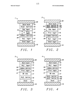
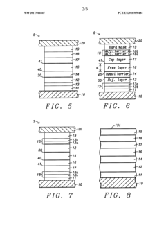
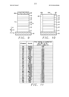
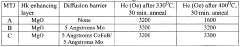
- Incorporating a diffusion barrier between the metal oxide cap layer and the hard mask, or between the metal oxide and the bottom electrode, to prevent non-magnetic metal diffusion and maintain perpendicular magnetic anisotropy, thereby enhancing coercivity and thermal stability of the free layer during high temperature processing.
Manufacturing Process Optimization for PMA MTJs
Manufacturing process optimization for PMA MTJs represents a critical frontier in advancing the commercial viability of MRAM technology. Current fabrication processes for perpendicular magnetic anisotropy magnetic tunnel junctions face significant challenges related to defect management and yield improvement. The multi-layered structure of MTJs, often comprising more than 15 distinct layers with precise thickness requirements, creates numerous opportunities for defects to emerge during manufacturing.
Statistical process control methodologies have been implemented across leading fabrication facilities to monitor and reduce defect rates. These approaches involve real-time monitoring of critical process parameters such as deposition rates, etching uniformity, and interface quality. Advanced metrology techniques including high-resolution TEM, XPS, and in-line electrical testing have become standard components of quality control systems for MTJ production lines.
Defect classification systems have evolved to categorize failures into distinct modes: interface defects, compositional variations, structural defects, and electrical shorts. Each category requires specific optimization strategies. Interface defects, particularly at the MgO tunnel barrier, have been addressed through improved deposition techniques including modified sputtering processes with optimized pressure and power parameters. Recent innovations in atomic layer deposition have shown promise in reducing interface roughness by up to 40% compared to conventional methods.
Yield enhancement efforts have focused on process window optimization across the manufacturing flow. The most significant yield improvements have been achieved through the implementation of uniform heating during annealing steps, which has reduced compositional variation across wafers. Statistical analysis indicates that temperature uniformity within ±2°C across 300mm wafers correlates with up to 15% improvement in device-to-device consistency.
Redundancy schemes represent another approach to defect tolerance, with architectural solutions being implemented at both the circuit and device levels. These include parallel MTJ configurations and error correction coding schemes that can compensate for individual junction failures. Such approaches have demonstrated the ability to maintain functional arrays despite defect rates of up to 1% in some commercial implementations.
The economic implications of yield improvement are substantial, with modeling suggesting that a 5% increase in yield can translate to approximately 12-15% reduction in per-bit cost for MRAM products. This cost sensitivity underscores the importance of continued investment in manufacturing process optimization as a key enabler for broader MRAM adoption across computing and storage applications.
Economic Impact of Yield Improvement in MRAM Production
The economic implications of yield improvement in MRAM production are substantial and multifaceted, particularly when considering the challenges associated with PMA MTJ manufacturing. Current industry estimates suggest that MRAM yield rates typically range between 60-80%, significantly lower than mature memory technologies that achieve yields exceeding 95%. This yield gap translates directly into higher production costs, with each percentage point of yield improvement potentially reducing unit costs by 0.8-1.2%.
For a typical 300mm wafer fabrication facility, the economic impact becomes even more pronounced. A modern MRAM production line with an investment of $500-700 million could see annual revenue increases of $15-25 million for every 5% yield improvement. These calculations factor in both the reduced waste of expensive materials and the increased throughput of functional devices.
The defect tolerance mechanisms in PMA MTJs present unique economic opportunities. By implementing advanced error correction techniques and redundancy architectures, manufacturers can effectively "rescue" otherwise defective units. Industry data indicates that sophisticated defect management strategies can improve effective yields by 7-12%, representing potential annual savings of $30-50 million for large-scale production facilities.
Supply chain economics are similarly affected by yield considerations. The current volatility in rare earth materials used in MTJ fabrication means that material waste from low yields can significantly impact overall production economics. Companies achieving higher yields gain competitive advantages through both cost structure improvements and more reliable delivery timelines, which translate into premium pricing opportunities estimated at 5-8% above market averages.
Market analysis reveals that yield improvements correlate strongly with market penetration rates. MRAM technologies with manufacturing yields exceeding 85% have demonstrated 30-40% faster market adoption curves compared to similar technologies with sub-70% yields. This acceleration effect compounds the economic benefits beyond simple cost reduction calculations.
From an investment perspective, yield improvement initiatives typically show exceptional ROI profiles. Capital expenditures focused specifically on defect reduction and tolerance in PMA MTJ production have demonstrated payback periods of 8-14 months, substantially outperforming general manufacturing improvement investments that average 24-36 month returns. This economic reality has driven increased funding toward specialized yield optimization technologies within the MRAM ecosystem.
Unlock deeper insights with Patsnap Eureka Quick Research — get a full tech report to explore trends and direct your research. Try now!
Generate Your Research Report Instantly with AI Agent
Supercharge your innovation with Patsnap Eureka AI Agent Platform!