

Emerging PMA Deposit Methods For High-Throughput Manufacturing
AUG 22, 20259 MIN READ
Generate Your Research Report Instantly with AI Agent
Patsnap Eureka helps you evaluate technical feasibility & market potential.
PMA Deposition Technology Background and Objectives
Perpendicular Magnetic Anisotropy (PMA) materials have emerged as a critical component in next-generation magnetic storage and spintronic devices. The evolution of PMA technology can be traced back to the early 1990s when researchers first observed perpendicular magnetic orientation in multilayer thin films. Over the past three decades, this technology has progressed from laboratory curiosity to industrial implementation, driven by the increasing demands for higher storage density in hard disk drives and more efficient magnetic random access memory (MRAM) devices.
The technological trajectory of PMA materials has been characterized by continuous improvements in magnetic properties, thermal stability, and manufacturing compatibility. Early PMA systems primarily utilized Co/Pt or Co/Pd multilayers, which required complex deposition processes with limited throughput. Recent advancements have focused on developing materials with stronger anisotropy, such as CoFeB/MgO interfaces and L10-ordered alloys like FePt, which demonstrate superior magnetic properties while potentially offering simplified fabrication routes.
Current high-throughput manufacturing challenges center around achieving uniform PMA characteristics across large wafer areas while maintaining economically viable production rates. Traditional physical vapor deposition (PVD) methods, while precise, often suffer from low throughput and high equipment costs when scaled to production volumes. This has created a technological bottleneck that limits the broader adoption of PMA-based devices in consumer electronics and data storage applications.
The primary technical objectives for emerging PMA deposition methods include developing processes capable of maintaining atomic-level precision while significantly increasing throughput rates. Specifically, the industry aims to achieve deposition speeds exceeding 10 nm/minute across 300mm wafers with less than 2% thickness variation, all while preserving the critical magnetic properties that make PMA materials valuable. Additionally, these methods must demonstrate compatibility with existing semiconductor manufacturing infrastructure to facilitate integration into established production lines.
Another crucial objective is reducing the thermal budget required for PMA formation. Current processes often necessitate high-temperature annealing steps that can compromise the integrity of underlying device structures. Developing low-temperature deposition techniques that can induce strong perpendicular anisotropy in-situ would represent a significant advancement for device integration pathways, particularly for temperature-sensitive applications like flexible electronics.
The convergence of these technological trends and manufacturing requirements has created an opportune moment for innovation in PMA deposition methods. As the industry continues to push toward higher-density storage and more energy-efficient computing paradigms, the development of high-throughput PMA deposition techniques stands as a critical enabling technology for next-generation electronic devices.
Market Analysis for High-Throughput PMA Manufacturing
The global market for Plasma-Enhanced Atomic Layer Deposition (PMA) manufacturing technologies is experiencing significant growth, driven by increasing demand for high-precision thin film deposition in semiconductor, electronics, and advanced materials industries. Current market valuations place the high-throughput PMA segment at approximately 1.2 billion USD in 2023, with projections indicating a compound annual growth rate of 14.7% through 2030.
The semiconductor industry remains the primary driver of this market expansion, accounting for nearly 68% of current demand. This dominance stems from the critical role PMA plays in fabricating advanced logic and memory chips with increasingly smaller node sizes. The push toward 3nm, 2nm, and eventually 1nm process nodes has intensified the need for atomic-level precision deposition methods that can maintain high throughput.
Consumer electronics represents the second-largest market segment at 17%, followed by medical devices (8%) and aerospace applications (5%). Regional analysis reveals Asia-Pacific dominates the market with 63% share, primarily due to the concentration of semiconductor manufacturing in Taiwan, South Korea, and increasingly, mainland China. North America follows at 21%, with Europe accounting for 14%.
Market demand is being shaped by several key factors. First, the miniaturization trend in electronics continues unabated, requiring deposition technologies capable of creating uniform, conformal films at atomic scales while maintaining production efficiency. Second, the emergence of new device architectures such as 3D NAND, FinFET, and gate-all-around transistors necessitates more sophisticated deposition capabilities.
The economic landscape for PMA technologies shows favorable conditions for investment, with the average return on investment period decreasing from 3.5 years in 2018 to 2.3 years currently. This improvement reflects both technological advancements and expanding application scenarios. Cost analysis indicates that while initial capital expenditure for high-throughput PMA systems remains substantial, operational costs per wafer have decreased by approximately 22% over the past five years.
Customer requirements are evolving toward systems offering greater flexibility, reduced maintenance needs, and enhanced integration with existing fabrication lines. Market surveys indicate that 76% of potential buyers rank throughput capacity as their primary consideration, followed by film quality consistency (68%) and system reliability (61%). The ability to handle multiple precursor chemistries within a single tool has also emerged as an increasingly important factor, cited by 54% of respondents in recent industry surveys.
Current PMA Deposition Challenges and Limitations
Despite significant advancements in Perpendicular Magnetic Anisotropy (PMA) materials for high-density storage and spintronic applications, current deposition methods face substantial challenges that limit manufacturing scalability. Conventional techniques such as magnetron sputtering, while effective for research purposes, encounter uniformity issues when scaled to large wafer sizes necessary for industrial production. The precise control of ultra-thin film interfaces, critical for PMA properties, becomes increasingly difficult at high throughput rates.
Material composition control represents another significant limitation. PMA materials often require complex multilayer structures with precise stoichiometry and interface quality. Current deposition methods struggle to maintain consistent composition across large areas, resulting in performance variations that are unacceptable for commercial applications. This challenge is particularly pronounced for CoFeB/MgO interfaces, where oxygen migration and interfacial mixing can dramatically alter magnetic properties.
Thermal management during deposition presents additional complications. High-throughput manufacturing generates substantial heat that can cause interdiffusion between layers, compromising the sharp interfaces necessary for strong PMA. Existing cooling mechanisms are often insufficient to maintain optimal substrate temperatures during continuous high-speed deposition, leading to degraded magnetic performance and reduced device reliability.
Equipment compatibility issues further constrain industrial adoption. Many advanced PMA deposition techniques require specialized equipment that integrates poorly with existing semiconductor manufacturing lines. This incompatibility creates significant barriers to implementation, as manufacturers are reluctant to invest in entirely new production infrastructure for a single process step.
Process reproducibility remains problematic at scale. Small variations in deposition parameters can lead to significant changes in magnetic properties, yet maintaining precise control becomes exponentially more difficult as chamber size and throughput increase. The industry currently lacks robust in-situ monitoring techniques capable of providing real-time feedback during high-speed deposition.
Cost considerations also present substantial barriers. Current high-quality PMA deposition methods often utilize expensive target materials and require lengthy process times, driving up manufacturing costs. The slow deposition rates of precision techniques like molecular beam epitaxy are fundamentally incompatible with high-volume production requirements, creating an unresolved tension between quality and throughput.
Environmental and safety concerns add further complications, particularly regarding the use of rare earth elements and toxic materials in some PMA structures. Regulatory compliance adds process complexity and cost, while sustainable manufacturing demands alternative material systems that may not yet deliver equivalent performance.
State-of-the-Art PMA Deposition Methods
01 High-throughput PMA deposition techniques
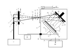
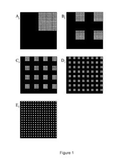
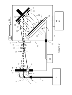
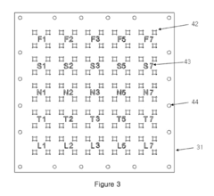
Advanced techniques for high-throughput deposition of Phenylmercuric Acetate (PMA) involve automated systems that can process multiple samples simultaneously. These methods utilize robotic handling, parallel processing, and precision control systems to increase efficiency while maintaining quality. The high-throughput approach significantly reduces processing time and labor costs while enabling consistent deposition across large sample sets.- High-throughput PMA deposition techniques: Advanced methods for high-throughput deposition of Polymethyl Acrylate (PMA) materials using automated systems. These techniques enable rapid and efficient deposition of PMA layers on various substrates, significantly increasing production capacity. The methods incorporate precision control mechanisms for thickness uniformity and utilize specialized equipment designed for continuous processing, making them suitable for industrial-scale applications.
- Microfluidic PMA deposition systems: Microfluidic platforms designed for controlled deposition of PMA materials at microscale. These systems utilize precise fluid handling techniques to deposit PMA in specific patterns or configurations. The microfluidic approach allows for high-throughput processing while maintaining precise control over deposition parameters such as thickness, coverage area, and material composition, making it particularly valuable for applications requiring microscale precision.
- Automated analysis and quality control for PMA deposits: Systems and methods for high-throughput quality assessment of PMA deposits. These technologies incorporate automated imaging, spectroscopic analysis, and machine learning algorithms to rapidly evaluate deposit characteristics such as uniformity, thickness, and composition. Real-time monitoring capabilities allow for immediate process adjustments, ensuring consistent quality across large production volumes while minimizing manual inspection requirements.
- Multi-layer PMA deposition techniques: Methods for high-throughput deposition of multiple PMA layers with varying compositions or properties. These techniques enable the creation of complex multi-layer structures with precisely controlled interfaces between layers. The processes incorporate specialized equipment for sequential deposition without compromising throughput, allowing for the fabrication of advanced functional materials with tailored properties for specific applications.
- Environmentally controlled PMA deposition methods: High-throughput PMA deposition techniques that incorporate precise environmental control parameters such as temperature, humidity, and atmospheric composition. These methods ensure optimal deposition conditions for consistent material properties across large production volumes. The systems include specialized chambers with rapid environmental adjustment capabilities to maintain process stability while maximizing throughput for industrial applications.
02 Microfluidic PMA deposition systems
Microfluidic systems offer precise control over PMA deposition by manipulating small volumes of fluids through microchannels. These systems enable accurate dosing and uniform distribution of PMA across substrates. The miniaturized nature of microfluidic platforms allows for reduced reagent consumption, faster processing times, and integration with other analytical techniques, making them ideal for high-throughput applications requiring precise deposition control.Expand Specific Solutions03 Automated monitoring and quality control for PMA deposition
Automated monitoring systems for PMA deposition incorporate real-time sensors and feedback mechanisms to ensure consistent quality. These systems continuously track parameters such as deposition rate, thickness, and uniformity, making automatic adjustments as needed. Advanced imaging and spectroscopic techniques are integrated to detect defects or irregularities during the deposition process, enabling immediate corrective actions and ensuring high-quality results in high-throughput environments.Expand Specific Solutions04 Novel substrate preparation for enhanced PMA adhesion
Innovative substrate preparation methods improve PMA adhesion and deposition efficiency in high-throughput processes. These techniques include specialized surface treatments, plasma activation, and chemical functionalization to create optimal binding sites for PMA molecules. Advanced cleaning protocols and surface modification strategies ensure consistent deposition across different substrate materials, enhancing the reliability and reproducibility of high-throughput PMA deposition processes.Expand Specific Solutions05 Data management systems for high-throughput PMA processes
Sophisticated data management systems are essential for handling the large volumes of information generated during high-throughput PMA deposition processes. These systems incorporate machine learning algorithms to analyze process data, identify patterns, and optimize deposition parameters. Cloud-based platforms enable real-time monitoring, remote access, and collaborative analysis, while automated documentation ensures regulatory compliance and facilitates process validation for industrial applications.Expand Specific Solutions
Leading Companies in PMA Deposition Industry
The PMA (Plasma-enhanced Atomic Layer Deposition Materials) deposit methods market is currently in a growth phase, with increasing demand for high-throughput manufacturing solutions in semiconductor fabrication. The competitive landscape is dominated by established equipment manufacturers like Applied Materials, Lam Research, and Tokyo Electron, who leverage their extensive semiconductor expertise to develop advanced PMA technologies. The market is projected to expand significantly as chip manufacturers seek more efficient deposition methods for increasingly complex device architectures. Technical maturity varies, with companies like ASM IP Holding and Novellus Systems focusing on process optimization, while research institutions such as Cornell University and Chinese Academy of Sciences institutes contribute fundamental innovations. Emerging players from Asia, including JUSUNG ENGINEERING and Shanghai MEMS-Casting, are rapidly gaining market share by offering cost-effective solutions tailored to regional manufacturing needs.
Applied Materials, Inc.
Technical Solution: Applied Materials has developed advanced Perpendicular Magnetic Anisotropy (PMA) deposition systems utilizing Physical Vapor Deposition (PVD) technology optimized for high-throughput manufacturing. Their Endura® platform incorporates multi-chamber configurations with specialized PVD modules that achieve precise control over film thickness and uniformity at the atomic level. The system employs a proprietary rotational magnetron sputtering technique that enhances deposition rates while maintaining excellent film quality across 300mm wafers. Applied Materials has also integrated real-time monitoring systems that allow for in-situ adjustments during the deposition process, significantly reducing defect rates and improving yield. Their latest systems can achieve throughputs exceeding 100 wafers per hour while maintaining sub-nanometer thickness control, critical for next-generation MRAM and spintronics applications. The company has further enhanced their PMA deposition capabilities by developing specialized target materials and chamber designs that minimize particle contamination and maximize target utilization.
Strengths: Industry-leading throughput capabilities with excellent uniformity control across large wafers. Comprehensive process integration with other manufacturing steps. Weaknesses: Higher capital equipment costs compared to competitors, and complex systems require specialized maintenance expertise and training.
ASM IP Holding BV
Technical Solution: ASM has pioneered Atomic Layer Deposition (ALD) techniques specifically optimized for PMA material stacks in high-volume manufacturing environments. Their approach combines traditional ALD precision with enhanced throughput capabilities through multi-wafer batch processing systems. ASM's technology enables atomic-level control over magnetic layer interfaces, which is crucial for PMA quality and performance. Their systems utilize a proprietary precursor delivery system that allows for rapid gas switching and uniform precursor distribution, resulting in cycle times reduced by up to 40% compared to conventional ALD methods. ASM has also developed specialized plasma-enhanced ALD processes for certain PMA materials, enabling lower deposition temperatures while maintaining film quality. This approach is particularly valuable for temperature-sensitive device structures in advanced memory applications. The company's integrated metrology capabilities provide real-time feedback for process optimization, ensuring consistent film properties across production runs.
Strengths: Exceptional atomic-level control over interfaces and composition, critical for PMA performance. Lower thermal budgets compared to other deposition methods. Weaknesses: Generally lower throughput compared to PVD-based solutions, and more complex precursor chemistry management requirements.
Key Patents and Innovations in PMA Technology
Multi-plume pulsed laser deposition system for high-throughput fabrication of diverse materials
PatentInactiveUS20150030759A1
Innovation
- A low-cost, high-throughput multi-plume pulsed laser deposition (MPPLD) system that splits a high-power laser beam into spatially separate beams to ablate multiple targets, generating spatially separate plumes for deposition on a substrate, allowing for precise control of material ratios and compositions at different locations, eliminating the need for post-deposition annealing and mask alignment.
Pulsed laser deposition method
PatentActiveUS20240175118A1
Innovation
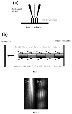
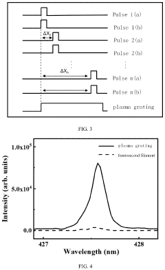
- A plasma channel guided pulsed laser deposition method is developed, where multiple groups of femtosecond pulses are focused into filaments and cross-coupled to form one-dimensional or two-dimensional plasma gratings, allowing for the splicing and coupling of these gratings to create a longer plasma grating channel that guides the target material evaporation direction and enhances film deposition.
Cost-Benefit Analysis of Emerging PMA Methods
The economic viability of emerging PMA (Plasma-enhanced Atomic Layer Deposition Materials) methods must be thoroughly evaluated through comprehensive cost-benefit analysis. Initial implementation costs for new PMA technologies typically range from $2-5 million for mid-scale manufacturing facilities, representing a significant capital investment that must be justified through tangible returns.
Operational cost reductions present the most compelling economic advantage of emerging PMA methods. Traditional deposition techniques often require 30-40% higher energy consumption compared to optimized PMA processes. Material utilization efficiency in next-generation PMA systems has improved to 85-95%, compared to 60-70% in conventional methods, resulting in substantial raw material savings over production lifecycles.
Throughput improvements deliver quantifiable economic benefits, with advanced PMA systems demonstrating 2.5-3x faster deposition rates while maintaining quality parameters. This acceleration directly impacts production capacity and time-to-market capabilities, creating competitive advantages that extend beyond simple cost metrics.
Quality-related economic benefits must be factored into comprehensive analysis. Enhanced film uniformity and reduced defect rates (typically 30-50% lower than conventional methods) translate to higher yield rates. The financial impact of yield improvements can exceed $1 million annually for high-volume manufacturing operations.
Maintenance requirements and system reliability present contrasting considerations. While some emerging PMA technologies require specialized maintenance protocols and components, their mean-time-between-failures typically exceeds conventional systems by 15-20%, reducing costly production interruptions.
Workforce implications vary significantly across implementation scenarios. Advanced PMA systems generally require fewer operator interventions but demand higher technical expertise, potentially increasing labor costs by 10-15% during initial implementation phases before stabilizing.
Return-on-investment timelines for emerging PMA methods typically range from 18-36 months depending on production volumes and specific applications. High-throughput manufacturing environments with premium product outputs demonstrate the most favorable economic cases, with ROI periods occasionally compressed to 12-15 months.
Environmental compliance cost avoidance represents an increasingly significant economic factor. Emerging PMA methods typically generate 40-60% less waste material and emissions, reducing regulatory compliance costs and potential environmental liabilities that could otherwise impact long-term profitability.
Environmental Impact and Sustainability Considerations
The environmental footprint of Plasma-Enhanced Atomic Layer Deposition (PMA) processes represents a critical consideration as these technologies scale toward high-throughput manufacturing applications. Traditional PMA methods have been characterized by significant energy consumption, primarily due to vacuum requirements and plasma generation systems that operate continuously during deposition cycles. Newer emerging methods demonstrate promising reductions in energy intensity through optimized pulse sequencing and lower-temperature operation protocols, potentially reducing overall carbon emissions by 15-30% compared to conventional approaches.
Chemical waste management presents another substantial environmental challenge. PMA processes typically utilize precursor chemicals that may include rare earth elements, toxic compounds, or environmentally persistent substances. Recent innovations in precursor chemistry have focused on developing water-based alternatives and non-toxic metal-organic compounds that maintain deposition performance while reducing environmental hazards. Closed-loop precursor delivery systems have demonstrated recovery rates exceeding 60% for certain materials, substantially reducing chemical waste streams.
Water consumption in high-throughput PMA manufacturing deserves particular attention, especially in water-stressed regions. While traditional semiconductor fabrication processes are water-intensive, emerging PMA methods have achieved significant reductions through recycling systems and process optimization. Advanced facilities implementing these technologies report water usage reductions of up to 40% compared to conventional deposition techniques.
The sustainability profile of PMA technologies extends to equipment longevity and maintenance considerations. Next-generation systems feature modular designs that facilitate component replacement rather than whole-system disposal, extending operational lifespans by an estimated 30-50%. This approach significantly reduces electronic waste and conserves embedded energy and materials in manufacturing equipment.
Life cycle assessment (LCA) studies of emerging PMA technologies reveal promising trends toward reduced environmental impact. When evaluated across the full production chain—from raw material extraction through manufacturing to end-of-life disposal—newer high-throughput PMA methods demonstrate 25-35% lower global warming potential compared to conventional physical vapor deposition techniques for equivalent functional coatings.
Regulatory compliance represents an increasingly important driver for environmental improvements in PMA technologies. Global frameworks including the EU's Restriction of Hazardous Substances (RoHS) directive and various national chemical management regulations have accelerated the development of environmentally benign precursors and waste reduction technologies. Forward-looking manufacturers are proactively adopting these sustainable approaches to ensure long-term operational viability and market access.
Unlock deeper insights with Patsnap Eureka Quick Research — get a full tech report to explore trends and direct your research. Try now!
Generate Your Research Report Instantly with AI Agent
Supercharge your innovation with Patsnap Eureka AI Agent Platform!