Comparative Study: STT-MRAM Vs SOT-MRAM With PMA Layers
AUG 22, 20259 MIN READ
Generate Your Research Report Instantly with AI Agent
Patsnap Eureka helps you evaluate technical feasibility & market potential.
MRAM Technology Evolution and Objectives
Magnetoresistive Random Access Memory (MRAM) has emerged as a promising non-volatile memory technology, evolving significantly since its conceptualization in the late 1980s. The initial MRAM designs utilized in-plane magnetic anisotropy (IMA), which faced scalability challenges due to high switching currents and thermal stability issues. The introduction of perpendicular magnetic anisotropy (PMA) in the early 2010s marked a pivotal advancement, enabling higher density integration and improved energy efficiency.
The evolution of MRAM technology has been characterized by two major writing mechanisms: Spin-Transfer Torque (STT) and Spin-Orbit Torque (SOT). STT-MRAM, commercialized around 2016, represented the first generation of scalable MRAM technology. It utilizes spin-polarized current passing through the magnetic tunnel junction (MTJ) to switch the free layer magnetization. While effective, STT-MRAM faces endurance limitations due to the stress on the tunnel barrier during write operations.
SOT-MRAM emerged as a potential solution to STT-MRAM's limitations, employing a three-terminal structure where write and read paths are separated. This separation fundamentally addresses the endurance concerns by eliminating tunnel barrier degradation during write operations. The integration of PMA layers in both STT and SOT-MRAM has been crucial for enhancing thermal stability and reducing critical switching current.
The technological trajectory of MRAM has been driven by the semiconductor industry's demand for memory solutions that combine non-volatility, high speed, unlimited endurance, and CMOS compatibility. The development of advanced materials with strong PMA properties, such as CoFeB/MgO interfaces, Ta/CoFeB/MgO stacks, and more recently, synthetic antiferromagnets (SAFs), has been instrumental in pushing MRAM performance boundaries.
The primary objectives of current MRAM research focus on achieving higher density integration, reducing power consumption, improving switching reliability, and enhancing data retention. For STT-MRAM, key goals include reducing the critical switching current while maintaining thermal stability. For SOT-MRAM, objectives center on optimizing the spin Hall effect efficiency, reducing device footprint, and simplifying the integration process with standard CMOS technology.
This comparative study aims to provide a comprehensive analysis of STT-MRAM and SOT-MRAM technologies with PMA layers, evaluating their respective strengths, limitations, and potential for future applications. The assessment will consider performance metrics such as switching energy, write latency, endurance, retention time, and scalability to sub-20nm nodes, providing insights into which technology might better serve specific application domains in the evolving memory landscape.
Market Analysis for Next-Generation Memory Solutions
The next-generation non-volatile memory market is experiencing significant growth, driven by increasing demands for faster, more energy-efficient, and reliable memory solutions across various sectors. The global market for emerging non-volatile memory technologies, including MRAM variants, is projected to reach $13.7 billion by 2026, with a compound annual growth rate of 29.4% from 2021 to 2026.
STT-MRAM (Spin-Transfer Torque Magnetic Random Access Memory) has already established a foothold in the commercial market, with companies like Everspin Technologies reporting annual revenues exceeding $50 million from MRAM products. The technology has found applications in automotive, industrial automation, and enterprise storage systems due to its combination of non-volatility and SRAM-like performance characteristics.
SOT-MRAM (Spin-Orbit Torque MRAM) with PMA (Perpendicular Magnetic Anisotropy) layers represents the next evolution in magnetic memory technology, promising even lower power consumption and higher endurance than STT-MRAM. Market analysts predict that once commercialized, SOT-MRAM could capture up to 15% of the specialty memory market within five years of mass production.
The demand for these advanced memory technologies is particularly strong in data centers, where energy efficiency is paramount. With data centers consuming approximately 1-2% of global electricity, memory solutions that reduce power consumption while maintaining performance are highly valued. Both STT-MRAM and SOT-MRAM offer significant power savings compared to conventional DRAM, with SOT-MRAM potentially reducing memory-related power consumption by up to 70%.
In the automotive sector, the transition to electric and autonomous vehicles is creating demand for reliable, temperature-resistant, and radiation-hardened memory. The automotive memory market is expected to grow at 23% annually through 2025, with MRAM technologies positioned to capture a significant portion due to their inherent advantages in harsh operating environments.
Consumer electronics represents another substantial market opportunity, particularly as edge computing and AI applications become more prevalent in smartphones and IoT devices. The reduced write latency and lower power consumption of SOT-MRAM make it particularly attractive for battery-powered devices, potentially extending operational time between charges by 20-30% compared to current solutions.
Geographically, North America and Asia-Pacific dominate the advanced memory market, with major investments in both regions. Japan, South Korea, and Taiwan are leading in manufacturing capabilities, while the United States maintains an edge in research and development. European markets are showing increased interest, particularly for industrial and automotive applications, with projected market growth of 32% annually through 2025.
STT-MRAM and SOT-MRAM Technical Challenges
Despite significant advancements in MRAM technologies, both STT-MRAM and SOT-MRAM face substantial technical challenges that limit their widespread commercial adoption. For STT-MRAM, one of the primary obstacles is the high write current density requirement, typically in the range of 10^6-10^7 A/cm², which leads to considerable power consumption and potential reliability issues. This high current density creates thermal stability concerns and can accelerate device degradation through electromigration effects in the tunnel barrier.
The read-write path separation presents another critical challenge for STT-MRAM. Since both operations utilize the same current path through the magnetic tunnel junction (MTJ), there exists an inherent trade-off between read disturbance and write efficiency. Increasing the tunnel magnetoresistance (TMR) ratio to improve read performance often requires thicker MgO barriers, which subsequently increases the write current requirements.
Scalability remains problematic for STT-MRAM below the 20nm node. As device dimensions shrink, maintaining sufficient thermal stability factor (Δ) while simultaneously reducing the switching current becomes increasingly difficult. This fundamental physics constraint creates a scaling bottleneck that engineers continue to struggle with.
SOT-MRAM, while addressing some of STT-MRAM's limitations, introduces its own set of challenges. The three-terminal device structure, while beneficial for separating read and write paths, increases the cell area significantly compared to STT-MRAM. This larger footprint reduces memory density and presents integration challenges in high-density memory applications.
The write mechanism in SOT-MRAM requires an external magnetic field or careful engineering of the spin-orbit coupling materials to achieve deterministic switching. This requirement adds complexity to both the device structure and the peripheral circuitry, increasing manufacturing costs and design complexity.
Material integration poses significant challenges for both technologies. For PMA (Perpendicular Magnetic Anisotropy) layers, achieving the optimal interface quality between the ferromagnetic layers and adjacent materials is critical for maintaining high perpendicular anisotropy. Defects, intermixing, and oxidation at these interfaces can severely degrade device performance.
Process compatibility with CMOS manufacturing presents another hurdle. The high-temperature steps in CMOS processing can damage the magnetic properties of MRAM materials, while the specialized materials used in MRAM (such as heavy metals for SOT) may introduce contamination risks to standard CMOS processes.
Reliability and endurance remain concerns for both technologies, with write errors, read disturbance, and time-dependent dielectric breakdown of the tunnel barrier limiting device lifetime. SOT-MRAM potentially offers better endurance due to reduced stress on the tunnel barrier, but still faces challenges in maintaining consistent performance over billions of write cycles.
Current PMA Layer Implementation Approaches
01 Structural differences between STT-MRAM and SOT-MRAM with PMA layers
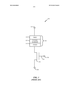
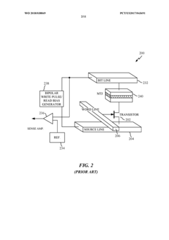
STT-MRAM and SOT-MRAM utilize different mechanisms for magnetization switching. STT-MRAM relies on spin-polarized current passing through the magnetic tunnel junction (MTJ) to switch the free layer, while SOT-MRAM uses spin-orbit torque generated by current flowing adjacent to the free layer. Both technologies can incorporate perpendicular magnetic anisotropy (PMA) layers to enhance thermal stability and reduce switching current. The structural differences impact device scaling, reliability, and integration capabilities in memory applications.- Comparison of STT-MRAM and SOT-MRAM switching mechanisms: STT-MRAM and SOT-MRAM utilize different switching mechanisms that affect their performance characteristics. STT-MRAM relies on spin-polarized current passing through the magnetic tunnel junction (MTJ) to switch the free layer, while SOT-MRAM uses spin-orbit torque generated by in-plane current in an adjacent heavy metal layer. This fundamental difference results in SOT-MRAM typically demonstrating faster switching speeds and lower write energy compared to STT-MRAM, though with different integration challenges.
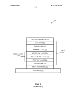
- PMA layer structure and material composition effects: The structure and material composition of perpendicular magnetic anisotropy (PMA) layers significantly impact the performance of both STT-MRAM and SOT-MRAM devices. PMA layers typically consist of CoFeB/MgO interfaces or multilayers with heavy metals. The thickness, interface quality, and material selection of these layers affect critical parameters such as thermal stability, switching current density, and retention time. Optimized PMA structures can enhance performance metrics in both memory technologies while maintaining the desired perpendicular orientation of magnetization.
- Thermal stability and retention characteristics: Thermal stability is a critical performance metric for both STT-MRAM and SOT-MRAM with PMA layers. SOT-MRAM generally offers better thermal stability due to the separation of read and write paths, which reduces disturbance issues. The thermal stability factor (Δ) in both technologies is influenced by the PMA layer properties, with higher anisotropy materials providing better data retention. However, increasing thermal stability often requires higher switching currents, creating a design trade-off that must be balanced differently in each technology.
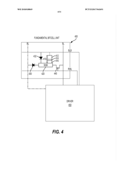
- Scalability and integration challenges: STT-MRAM and SOT-MRAM with PMA layers present different scalability and integration challenges. STT-MRAM has a more mature integration path with CMOS technology but faces scaling limitations due to the increasing current density required for switching at smaller nodes. SOT-MRAM offers better scalability potential due to its separate read/write paths and lower current requirements, but presents more complex integration challenges including the need for additional materials and process steps. The three-terminal design of SOT-MRAM requires more chip area compared to the two-terminal STT-MRAM design.
- Endurance and reliability comparison: SOT-MRAM demonstrates superior endurance and reliability compared to STT-MRAM due to its fundamental operating mechanism. The separation of read and write paths in SOT-MRAM reduces stress on the tunnel barrier, resulting in lower degradation over time and higher endurance cycles. STT-MRAM suffers from potential barrier breakdown issues as current passes through the MTJ during writing operations. Both technologies with PMA layers show improved reliability compared to their in-plane magnetized counterparts, but SOT-MRAM maintains a significant advantage in write endurance and long-term reliability.
02 Performance metrics comparison between STT-MRAM and SOT-MRAM
SOT-MRAM generally demonstrates faster switching speeds and lower write energy compared to STT-MRAM due to the separation of read and write paths. STT-MRAM typically offers higher density integration but faces reliability challenges at advanced nodes. With PMA layers, both technologies show improved thermal stability and retention time. SOT-MRAM exhibits better endurance due to reduced stress on the tunnel barrier during write operations, while STT-MRAM benefits from a simpler cell structure and established manufacturing processes.Expand Specific Solutions03 PMA layer materials and configurations for enhanced performance
Various materials and configurations are used to optimize PMA layers in both STT-MRAM and SOT-MRAM. Common PMA materials include CoFeB/MgO interfaces, multilayers of Co/Pt or Co/Pd, and rare earth-transition metal alloys. The thickness, composition, and interface quality of these layers significantly impact the magnetic properties. Advanced configurations incorporate synthetic antiferromagnetic structures, dual interface PMA, and engineered seed layers to enhance thermal stability, reduce switching current, and improve the overall performance of both memory technologies.Expand Specific Solutions04 Switching mechanisms and efficiency in PMA-based MRAM technologies
The switching mechanisms in STT-MRAM and SOT-MRAM with PMA layers differ fundamentally, affecting their efficiency. STT-MRAM switching occurs through spin transfer from a polarized current passing through the MTJ, while SOT-MRAM utilizes spin-orbit coupling effects from adjacent heavy metal layers. PMA-based devices show reduced critical switching current compared to in-plane magnetization designs. SOT-MRAM demonstrates more deterministic switching behavior and reduced stochasticity, while STT-MRAM benefits from a more compact cell design. The efficiency of both technologies is enhanced by optimizing the PMA layer properties and interface quality.Expand Specific Solutions05 Integration challenges and future prospects for PMA-based MRAM
Both STT-MRAM and SOT-MRAM with PMA layers face integration challenges in advanced semiconductor processes. STT-MRAM integration is more mature but faces scaling limitations due to the increasing current density required for switching at smaller nodes. SOT-MRAM offers better scalability but requires additional process steps and larger cell size. Future prospects include hybrid designs combining advantages of both technologies, development of novel PMA materials with enhanced thermal stability, and three-terminal device architectures. Research focuses on reducing switching current while maintaining reliability and data retention for embedded and standalone memory applications.Expand Specific Solutions
Key Industry Players in MRAM Technology
The STT-MRAM vs SOT-MRAM with PMA layers competitive landscape is evolving rapidly in an early growth market phase, with the global MRAM market expected to reach significant expansion in the coming years. While STT-MRAM has achieved commercial maturity with companies like Samsung, IBM, and TSMC leading production, SOT-MRAM remains in the research and development stage. Key players including Western Digital, IMEC, and Antaios are advancing SOT-MRAM technology, while academic institutions such as Beihang University and National University of Singapore contribute fundamental research. Chinese entities like Huawei and the Institute of Microelectronics of CAS are increasingly investing in both technologies, indicating a strategic focus on next-generation memory solutions with enhanced performance and energy efficiency.
Taiwan Semiconductor Manufacturing Co., Ltd.
Technical Solution: TSMC has developed sophisticated manufacturing processes for both STT-MRAM and SOT-MRAM with PMA layers. Their STT-MRAM technology utilizes advanced CoFeB/MgO-based MTJ stacks with carefully engineered synthetic antiferromagnetic (SAF) reference layers. TSMC's STT-MRAM process achieves write currents in the range of 50-100 μA with data retention exceeding 10 years at operating temperatures. For SOT-MRAM, TSMC employs heavy metal layers (primarily tungsten and platinum alloys) with optimized thicknesses (3-5nm) to maximize the spin Hall effect while maintaining compatibility with their CMOS processes. Their SOT-MRAM devices demonstrate switching speeds below 500 picoseconds with significantly reduced write energy compared to STT-MRAM. TSMC's PMA implementation includes precisely controlled Ta/CoFeB/MgO multilayers with CoFeB thicknesses around 1-1.2nm to maximize perpendicular anisotropy. They've also developed specialized annealing processes (typically 300-350°C) to crystallize the CoFeB layer while preserving the integrity of the MgO tunnel barrier.
Strengths: TSMC's manufacturing expertise enables industry-leading uniformity and yield for both MRAM technologies. Their integration capabilities allow seamless embedding of these memory technologies with logic circuits. Weaknesses: Their STT-MRAM still faces challenges with reliability during repeated write operations due to the high current density through the MTJ, while their SOT-MRAM requires larger cell areas due to the three-terminal configuration, limiting memory density compared to competing technologies.
Applied Materials, Inc.
Technical Solution: Applied Materials has developed comprehensive deposition and etching solutions specifically optimized for both STT-MRAM and SOT-MRAM with PMA layers. Their Endura® platform provides specialized PVD systems for the precise deposition of magnetic multilayers with thickness control at the angstrom level, critical for PMA formation. For STT-MRAM, Applied Materials offers integrated solutions for creating high-quality CoFeB/MgO interfaces with minimal defects, achieving tunnel magnetoresistance ratios exceeding 200%. Their proprietary deposition technology enables the creation of synthetic antiferromagnetic reference layers with enhanced stability. For SOT-MRAM, Applied Materials has developed specialized deposition techniques for heavy metal layers (W, Pt, Ta) with optimized grain structure and interface quality to maximize spin-orbit coupling efficiency. Their PMA enhancement technology includes specialized Ta/CoFeB/MgO stack deposition with precise control of layer thicknesses and interfaces, along with optimized post-deposition annealing processes (typically 300-350°C) to promote crystallization while maintaining sharp interfaces.
Strengths: Applied Materials' equipment enables precise control over material interfaces and compositions, critical for both MRAM technologies. Their integrated approach allows for seamless manufacturing workflows from deposition through etching. Weaknesses: Their equipment solutions are primarily focused on the deposition and etching processes, requiring partnerships with device manufacturers for complete integration. The high cost of their specialized equipment can be prohibitive for smaller research facilities and startups exploring these technologies.
Critical Patents in STT-MRAM and SOT-MRAM
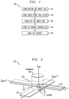
Spin orbit-torque magnetic random-access memory (SOT-MRAM) with cross-point spin hall effect (SHE) write lines and remote sensing read magnetic tunnel-junction (MTJ)
PatentActiveUS11869561B2
Innovation
- A cross-point SOT-MRAM cell design is implemented, featuring a first and second Spin Hall Effect (SHE) write line that are non-colinear, a cross-point free layer with dielectric isolation, and a remote sensing Magnetic Tunnel Junction (MTJ) to enable independent write and read operations without the need for STT-assisted writing, allowing for true cross-point architecture and improved integration density.
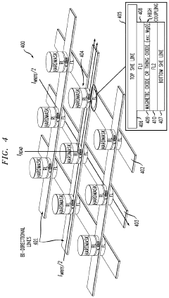
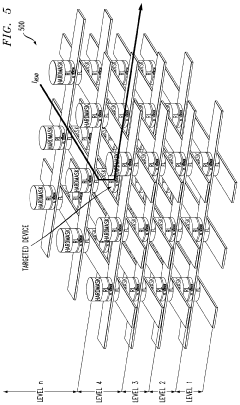
High speed, low power spin-orbit torque (SOT) assisted spin-transfer torque magnetic random access memory (STT-MRAM) bit cell array
PatentWO2018038849A1
Innovation
- A spin-orbit torque (SOT) assisted STT-MRAM bit cell array is developed, utilizing a perpendicular magnetic tunnel junction (pMTJ) with a spin-hall conductive material layer to generate a spin current and enhance switching speed and endurance by tuning the MTJ and spin-hall effect resistances, allowing for deterministic switching without external magnetic fields.
Energy Efficiency Comparison and Optimization
Energy efficiency represents a critical factor in the evaluation and implementation of emerging non-volatile memory technologies, particularly when comparing STT-MRAM and SOT-MRAM with Perpendicular Magnetic Anisotropy (PMA) layers. The fundamental energy consumption profiles of these technologies differ significantly due to their distinct switching mechanisms and architectural designs.
STT-MRAM utilizes spin-polarized current passing directly through the magnetic tunnel junction (MTJ) to switch the magnetization state. This direct current path results in relatively high energy consumption during write operations, typically ranging from 100-300 fJ per bit. The energy efficiency is further compromised by the requirement for higher current densities to ensure reliable switching, which increases exponentially as the switching time decreases below 10 ns.
In contrast, SOT-MRAM employs a separate write path through an adjacent heavy metal layer, decoupling the read and write operations. This architectural advantage enables SOT-MRAM to achieve significantly lower write energies, often in the range of 10-50 fJ per bit. The separation of read and write paths also eliminates the reliability concerns associated with the tunnel barrier degradation that plagues STT-MRAM.
The integration of PMA layers in both technologies has substantially improved their energy profiles. For STT-MRAM, PMA reduces the critical switching current by approximately 50-70% compared to in-plane magnetic anisotropy designs. Similarly, SOT-MRAM with PMA layers demonstrates enhanced thermal stability and reduced switching energy, with recent experimental demonstrations achieving sub-10 fJ per bit operations.
Optimization strategies for energy efficiency in these technologies follow multiple pathways. Material engineering approaches focus on developing MTJ stacks with lower damping constants and higher spin polarization. For STT-MRAM, reducing the Gilbert damping parameter from typical values of 0.01 to below 0.005 can decrease switching energy by up to 40%. For SOT-MRAM, enhancing the spin Hall angle in the heavy metal layer from 0.1 to 0.3 potentially reduces energy consumption by 60-70%.
Circuit-level optimizations also play a crucial role in energy efficiency. Implementing voltage-controlled magnetic anisotropy (VCMA) effects in conjunction with either switching mechanism can further reduce energy consumption by 30-50%. Advanced sensing schemes with lower read currents and shorter read pulses minimize the overall energy footprint during read operations, which is particularly beneficial for frequently accessed memory cells.
Fabrication Process Complexity Analysis
The fabrication process complexity of STT-MRAM and SOT-MRAM with PMA layers represents a critical factor in their commercial viability and scalability. Both technologies require sophisticated multi-layer deposition techniques, but with notable differences in their implementation challenges.
STT-MRAM fabrication involves a relatively mature process flow, benefiting from years of industrial refinement. The standard process requires approximately 12-15 deposition steps, including the formation of the magnetic tunnel junction (MTJ) stack with PMA layers. The critical challenge lies in achieving precise thickness control of the MgO tunnel barrier, typically requiring atomic-level precision of 1-2 nm. Additionally, the annealing process must be carefully controlled to establish the proper crystalline structure without compromising the integrity of the PMA layers.
SOT-MRAM, while sharing some fabrication steps with STT-MRAM, introduces additional complexity through the requirement of heavy metal layers for spin-orbit coupling. The fabrication typically demands 15-18 deposition steps, with more stringent requirements for interface quality between the heavy metal and ferromagnetic layers. The deposition of materials such as platinum, tungsten, or tantalum with precisely controlled thicknesses presents significant challenges.
Temperature sensitivity represents another key difference. STT-MRAM typically requires high-temperature annealing (300-350°C) to establish proper crystalline structure, which can potentially compromise the integrity of other device components. In contrast, SOT-MRAM may operate with lower annealing temperatures (250-300°C), offering better compatibility with back-end-of-line (BEOL) integration processes.
Etching processes also differ significantly between the two technologies. STT-MRAM typically employs ion beam etching (IBE) for the MTJ stack, which can lead to redeposition issues and sidewall damage. SOT-MRAM faces additional challenges in patterning the separate write and read paths, often requiring more complex lithography steps and potentially hybrid etching approaches combining reactive ion etching (RIE) and IBE.
From a manufacturing equipment perspective, both technologies require specialized PVD (Physical Vapor Deposition) tools capable of maintaining ultra-high vacuum conditions (10^-9 Torr or better). However, SOT-MRAM may demand more sophisticated multi-chamber systems to accommodate the additional material layers and more complex interfaces required for efficient spin-orbit torque generation.
The yield considerations also differ, with STT-MRAM showing current industrial yields of approximately 85-90% in leading fabs, while SOT-MRAM remains at research-level yields of 60-70% due to its earlier stage of development and more complex structure requirements.
Unlock deeper insights with Patsnap Eureka Quick Research — get a full tech report to explore trends and direct your research. Try now!
Generate Your Research Report Instantly with AI Agent
Supercharge your innovation with Patsnap Eureka AI Agent Platform!