PMA Materials For Neuromorphic And Non-Volatile Computing Architectures
AUG 22, 20259 MIN READ
Generate Your Research Report Instantly with AI Agent
Patsnap Eureka helps you evaluate technical feasibility & market potential.
PMA Materials Background and Research Objectives
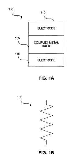
Perpendicular Magnetic Anisotropy (PMA) materials have emerged as a revolutionary class of materials in the field of spintronics and magnetic storage technologies over the past two decades. These materials exhibit magnetic anisotropy perpendicular to the film plane, offering significant advantages over traditional in-plane magnetized materials, particularly in terms of thermal stability and scalability. The evolution of PMA materials began with rare earth-transition metal alloys in the 1970s, progressing through Co/Pt and Co/Pd multilayers in the 1990s, to the current focus on CoFeB/MgO interfaces and other novel heterostructures.
The unique properties of PMA materials, including high anisotropy energy density, reduced critical current for magnetization switching, and excellent scalability, have positioned them as ideal candidates for neuromorphic computing architectures. These bio-inspired computing paradigms aim to mimic the brain's neural structure and function, offering potential solutions to the limitations of traditional von Neumann computing architectures, particularly in terms of energy efficiency and parallel processing capabilities.
Simultaneously, the non-volatile nature of PMA-based devices addresses the growing concern of power consumption in modern computing systems. Unlike conventional CMOS technology that requires constant power to maintain stored information, PMA-based memory and computing elements retain their state without power, significantly reducing energy requirements in standby mode and enabling instant-on functionality.
The primary technical objectives of this research include developing PMA materials with enhanced thermal stability at reduced dimensions (<10nm), achieving lower critical current densities for magnetization switching (<10^6 A/cm²), and improving the endurance of PMA-based devices (>10^15 cycles). Additionally, there is a focus on integrating these materials with CMOS technology to create hybrid systems that leverage the advantages of both technologies.
Another crucial research goal is to optimize the interface properties of PMA materials, as the perpendicular anisotropy often originates from interfacial effects. Understanding and controlling these interfaces at the atomic level is essential for developing next-generation devices with improved performance and reliability.
The long-term vision for PMA materials research extends beyond simple memory applications to complex neuromorphic architectures capable of learning and adaptation. This includes developing artificial synapses and neurons using PMA-based magnetic tunnel junctions (MTJs) that can emulate the plasticity and learning capabilities of biological neural systems while maintaining the energy efficiency and non-volatility inherent to these materials.
Market Analysis for Neuromorphic Computing Solutions
The neuromorphic computing market is experiencing significant growth, driven by increasing demand for AI applications and the limitations of traditional computing architectures. Current market valuations place the global neuromorphic computing sector at approximately $69 million in 2024, with projections indicating a compound annual growth rate (CAGR) of 89.1% through 2030, potentially reaching a market size of $1.78 billion.
Key market drivers include the exponential growth in data generation requiring more efficient processing solutions, rising adoption of AI and machine learning technologies across industries, and the inherent limitations of von Neumann architecture in handling complex neural network computations. The demand for energy-efficient computing solutions is particularly acute in edge computing applications, where power constraints are significant.
PMA (Perpendicular Magnetic Anisotropy) materials represent a critical component within this market landscape, offering promising capabilities for non-volatile memory solutions that can support neuromorphic architectures. The specific market segment for PMA-based neuromorphic solutions is currently nascent but demonstrates substantial growth potential, particularly as these materials overcome technical challenges related to energy efficiency and data persistence.
Industry analysis reveals distinct market segments emerging within neuromorphic computing: hardware infrastructure (chips, systems), software frameworks, and application-specific solutions. PMA materials primarily impact the hardware segment, where they enable novel memory architectures that more closely mimic biological neural systems.
Geographically, North America currently dominates the neuromorphic computing market with approximately 42% market share, followed by Europe (28%) and Asia-Pacific (24%). However, the Asia-Pacific region is experiencing the fastest growth rate, driven by substantial investments in semiconductor research and manufacturing capabilities, particularly in China, Japan, and South Korea.
From an end-user perspective, research institutions and technology companies currently represent the largest market segment, accounting for 65% of current implementations. However, automotive, healthcare, and defense sectors are rapidly increasing adoption rates, with projected CAGRs exceeding 95% in these verticals through 2028.
Market challenges include high initial development costs, technical complexity in implementation, and competition from alternative computing architectures. Despite these challenges, the unique advantages of PMA-based neuromorphic solutions—including ultra-low power consumption, non-volatility, and potential for high-density integration—position them favorably against competing technologies like memristors, phase-change memory, and conventional CMOS implementations.
Current Challenges in PMA Materials Development
Despite significant advancements in PMA (Perpendicular Magnetic Anisotropy) materials for neuromorphic and non-volatile computing architectures, several critical challenges continue to impede their widespread implementation. The primary obstacle remains the thermal stability-switching current dilemma, where enhancing thermal stability typically requires increasing the magnetic anisotropy, which consequently demands higher switching currents, resulting in excessive power consumption and potential device reliability issues.
Material interface engineering presents another significant challenge, as PMA properties are highly sensitive to the quality of interfaces between magnetic layers and adjacent materials. Even minor atomic interdiffusion or structural defects can dramatically degrade performance, making manufacturing consistency difficult to achieve at scale. This challenge becomes particularly acute when attempting to integrate PMA materials with CMOS technology in hybrid computing systems.
Scalability issues persist as device dimensions approach sub-10nm regimes, where quantum effects and edge irregularities begin to dominate magnetic behavior, often leading to unpredictable switching characteristics. The stochastic nature of switching at these dimensions creates reliability concerns for practical computing applications, particularly for neuromorphic systems requiring precise weight updates.
The endurance limitations of current PMA materials also present a substantial hurdle. Most existing materials demonstrate significant performance degradation after 10^6-10^9 switching cycles, falling short of the 10^15 cycles typically required for commercial memory applications. This degradation manifests as changes in switching current thresholds and increasing error rates over the device lifetime.
Manufacturing complexity represents another major challenge, as PMA materials often require precise deposition of multiple ultrathin layers with strict control over thickness, composition, and crystalline structure. Current industrial processes struggle to maintain the necessary uniformity across large wafers, resulting in significant device-to-device variations that complicate circuit design and operation.
Additionally, the temperature sensitivity of PMA materials restricts their operational range, with many materials exhibiting significant performance variations between room temperature and typical computing operating temperatures (60-85°C). This thermal instability complicates the design of robust neuromorphic systems that must function reliably across varying environmental conditions.
Finally, there remains a fundamental knowledge gap in understanding the complex interplay between material properties, device geometry, and switching dynamics, particularly in multi-layer structures designed for specialized neuromorphic functions. This limited theoretical foundation hampers the systematic development of optimized materials tailored specifically for neuromorphic computing applications.
Current PMA-Based Non-Volatile Memory Solutions
01 PMA materials for electronic devices
Polymethyl acrylate (PMA) materials are used in various electronic components due to their excellent electrical properties and thermal stability. These materials are incorporated into semiconductor devices, circuit boards, and other electronic applications. The unique properties of PMA materials make them suitable for enhancing performance and reliability in electronic systems.- PMA materials for electronic devices: Polymethyl acrylate (PMA) materials are used in various electronic components due to their excellent electrical properties and thermal stability. These materials are incorporated into semiconductor devices, display panels, and other electronic applications. The unique properties of PMA materials make them suitable for improving device performance, enhancing durability, and enabling advanced functionalities in modern electronics.
- PMA materials in communication systems: PMA (Physical Medium Attachment) materials are utilized in communication systems to facilitate data transmission and network connectivity. These materials are essential components in network infrastructure, enabling efficient signal processing and data exchange. They are designed to meet specific requirements for bandwidth, latency, and reliability in various communication protocols and systems.
- PMA materials for energy storage applications: Polymethyl acrylate (PMA) materials are employed in energy storage devices such as batteries and capacitors. These materials offer advantages including improved ion conductivity, enhanced electrode stability, and better cycle performance. The incorporation of PMA materials in energy storage applications contributes to higher energy density, longer lifespan, and improved safety characteristics.
- PMA materials in structural and construction applications: PMA (Polymer Modified Asphalt) materials are used in construction and infrastructure projects to enhance the performance of traditional building materials. These modified materials exhibit improved durability, weather resistance, and mechanical properties. Applications include road construction, waterproofing membranes, and structural reinforcements, where PMA materials provide extended service life and better resistance to environmental factors.
- PMA materials for biomedical applications: Polymethyl acrylate (PMA) materials are utilized in various biomedical applications due to their biocompatibility and versatile properties. These materials are incorporated into drug delivery systems, tissue engineering scaffolds, and medical devices. PMA materials can be engineered to provide controlled release of therapeutic agents, support cell growth, and interface with biological tissues, making them valuable in advanced healthcare technologies.
02 PMA materials in communication technology
PMA (Profile Management Application) materials are utilized in communication systems to manage user profiles and data across networks. These materials enable efficient data transmission, network management, and user authentication. The implementation of PMA materials in communication technology improves system reliability, security, and performance while facilitating seamless user experiences across different platforms.Expand Specific Solutions03 PMA materials for energy storage applications
Polymethyl acrylate (PMA) materials are employed in energy storage devices such as batteries and capacitors. These materials offer advantages including improved ion conductivity, enhanced electrode stability, and better cycle life. The incorporation of PMA materials in energy storage applications leads to higher energy density, faster charging capabilities, and extended operational lifetimes.Expand Specific Solutions04 PMA materials in structural applications
Polymer-modified asphalt (PMA) materials are used in construction and structural applications to enhance durability and performance. These materials exhibit improved resistance to deformation, cracking, and environmental degradation. The application of PMA materials in structural components results in extended service life, reduced maintenance requirements, and better overall structural integrity under various loading and environmental conditions.Expand Specific Solutions05 PMA materials for data management systems
Performance Management Application (PMA) materials are implemented in data management systems to optimize data processing, storage, and retrieval operations. These materials facilitate efficient monitoring, analysis, and management of system performance metrics. The integration of PMA materials in data management systems enables organizations to improve operational efficiency, enhance decision-making processes, and maintain optimal system performance under varying workloads.Expand Specific Solutions
Leading Organizations in Neuromorphic Computing Research
The neuromorphic and non-volatile computing architectures using PMA (Perpendicular Magnetic Anisotropy) materials market is in its early growth stage, characterized by intensive R&D activities rather than mass commercialization. The global market for neuromorphic computing is projected to reach $8-10 billion by 2028, with PMA-based solutions representing a significant segment. Major technology corporations including IBM, Samsung Electronics, Western Digital, and Micron Technology are leading commercial development, while academic institutions like Huazhong University of Science & Technology and Beihang University contribute fundamental research. The technology maturity remains at TRL 4-6, with IBM demonstrating the most advanced prototypes. Intel, TSMC, and Toshiba are also investing heavily in this space, indicating growing competitive intensity as the technology approaches commercialization readiness.
International Business Machines Corp.
Technical Solution: IBM has pioneered research in perpendicular magnetic anisotropy (PMA) materials for neuromorphic computing architectures. Their approach focuses on magnetic tunnel junctions (MTJs) with PMA that serve as artificial synapses and neurons. IBM's technology utilizes spin-transfer torque (STT) mechanisms in PMA-based materials to create non-volatile memory elements that mimic biological neural functions. Their research demonstrates that PMA-MTJs can achieve energy efficiency of approximately 1-10 fJ per synaptic operation, which is orders of magnitude lower than conventional CMOS implementations. IBM has also developed specialized programming techniques that enable precise control of the magnetic states, allowing for multi-level storage capabilities essential for neuromorphic weight representation. Their architecture incorporates these PMA-based devices into crossbar arrays that enable massively parallel matrix operations fundamental to neural network computation.
Strengths: Superior energy efficiency compared to CMOS implementations; non-volatility eliminates static power consumption; high endurance (>10^12 cycles) enables long-term operation. Weaknesses: Thermal stability challenges at smaller dimensions; variability between devices requires compensation circuits; integration with CMOS processes adds manufacturing complexity.
Samsung Electronics Co., Ltd.
Technical Solution: Samsung has developed advanced PMA-based spintronic devices for neuromorphic computing applications, focusing on vertical magnetic tunnel junctions (vMTJs) with perpendicular magnetic anisotropy. Their technology utilizes CoFeB/MgO interfaces to achieve strong PMA properties with thermal stability factors exceeding 60, ensuring reliable data retention. Samsung's approach incorporates domain wall motion in PMA materials to implement synaptic functionality, where the position of domain walls represents synaptic weight values. Their research demonstrates that these PMA-based devices can achieve switching energies below 100 fJ with write latencies under 10 ns, making them suitable for energy-efficient neuromorphic computing. Samsung has also pioneered integration techniques that allow these PMA devices to be embedded in the back-end-of-line (BEOL) process, enabling 3D integration with conventional CMOS circuits to create high-density neuromorphic systems with reported densities of up to 10^9 synaptic elements per cm².
Strengths: Excellent scalability with demonstrated functionality at sub-20nm dimensions; compatibility with existing semiconductor manufacturing infrastructure; high integration density potential through 3D stacking. Weaknesses: Relatively high programming currents compared to some competing technologies; reliability concerns under extreme temperature conditions; complex material stack requiring precise deposition control.
Key Innovations in PMA Materials Science
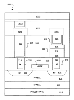
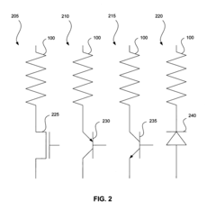
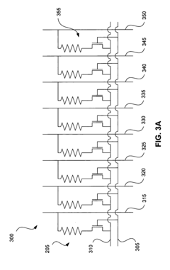
Non-volatile programmable memory
PatentInactiveEP1743340A1
Innovation
- A cross-point memory array design using a stacked configuration with two-terminal memory elements, where conductive array lines deliver voltage pulses to memory plugs, allowing for reduced footprint and increased memory capacity without increasing the array's size, by utilizing conductive materials like aluminum, copper, or ceramics for the array lines.
Non-volatile memory with a single transistor and resistive memory element
PatentInactiveUS7126841B2
Innovation
- The use of multi-resistive state materials as memory elements in non-volatile RAM, where the materials are deposited between electrodes with specific properties to minimize parasitic resistances and optimize resistive states, allowing for rapid switching and long-term retention, enabling the creation of efficient memory cells with controlled resistance values.
Energy Efficiency Considerations for PMA-Based Architectures
Energy efficiency represents a critical factor in the development and implementation of PMA (Perpendicular Magnetic Anisotropy) materials for neuromorphic and non-volatile computing architectures. The inherent non-volatility of PMA-based devices offers significant advantages in reducing static power consumption, as these materials can maintain their magnetic state without continuous power supply, effectively eliminating standby leakage power that plagues conventional CMOS technologies.
When examining the dynamic power consumption of PMA-based architectures, several key factors emerge. The energy required for switching magnetic states in PMA materials has been progressively decreasing, with recent advancements achieving sub-fJ/bit operations in certain configurations. This represents orders of magnitude improvement compared to early spintronic devices and approaches the efficiency levels necessary for large-scale integration.
Thermal stability remains a crucial consideration in PMA material selection and device design. The energy barrier that maintains the magnetic state must be sufficiently high to ensure data retention while remaining low enough to permit energy-efficient switching. This delicate balance directly impacts both reliability and power consumption metrics of the resulting computing architecture.
Integration with CMOS technology presents another dimension of energy efficiency considerations. The interface circuitry required for reading and writing PMA-based memory elements contributes significantly to the overall system power budget. Recent research has focused on developing more efficient sensing circuits and write drivers specifically optimized for the unique characteristics of PMA materials.
Scaling properties of PMA materials offer promising pathways for further energy efficiency improvements. As device dimensions decrease, the energy required for magnetic switching generally scales favorably, though challenges related to thermal stability and fabrication precision intensify. Research indicates that sub-10nm PMA devices can potentially operate at energy levels competitive with or superior to advanced CMOS memory technologies.
System-level architectural considerations must complement material-level optimizations to maximize energy efficiency. Neuromorphic computing architectures leveraging PMA materials can exploit event-driven computation paradigms, where processing occurs only when necessary, further reducing dynamic power consumption. Additionally, the co-location of memory and processing elements enabled by PMA-based devices significantly reduces energy-intensive data movement operations that dominate power consumption in conventional von Neumann architectures.
Scalability and Integration Challenges for Commercial Deployment
The commercialization of PMA (Perpendicular Magnetic Anisotropy) materials for neuromorphic and non-volatile computing architectures faces significant scalability and integration challenges that must be addressed before widespread adoption becomes feasible. Manufacturing PMA-based devices at scale requires overcoming process variability issues that currently plague prototype development. The intricate deposition processes for multilayer magnetic stacks demand precise control over layer thickness, interface quality, and composition uniformity across large wafer areas. Even minor variations can lead to inconsistent device performance, particularly problematic for neuromorphic systems where computational accuracy depends on predictable device behavior.
Integration with existing CMOS technology presents another substantial hurdle. While PMA materials offer excellent non-volatility and energy efficiency, their fabrication processes often require temperatures and conditions incompatible with back-end-of-line (BEOL) integration. This thermal budget constraint limits where in the manufacturing process these materials can be incorporated, potentially increasing production complexity and costs. Additionally, the magnetic properties of PMA materials can be affected by proximity to other circuit elements, necessitating careful design considerations for isolation and shielding.
Scaling challenges extend to the dimensional aspects as well. As device dimensions shrink below 20nm, quantum effects and thermal instabilities become increasingly prominent in PMA materials. The superparamagnetic limit—where magnetic domains become thermally unstable—poses a fundamental physical barrier that researchers must navigate through materials engineering or architectural innovations. Current laboratory demonstrations typically operate at dimensions significantly larger than would be required for competitive commercial memory or computing densities.
Signal integrity and noise management represent critical concerns for scaled deployment. PMA-based neuromorphic systems must maintain adequate signal-to-noise ratios when operating at the reduced energy levels that make them attractive alternatives to conventional computing. Cross-talk between adjacent magnetic elements can compromise computational accuracy, particularly in densely packed arrays necessary for commercial applications.
Reliability and endurance metrics for PMA materials still fall short of commercial requirements in many cases. While laboratory demonstrations show promising cycle counts, real-world applications demand consistent performance over trillions of operations under varying environmental conditions. Temperature sensitivity of magnetic properties introduces additional reliability concerns, potentially requiring sophisticated compensation mechanisms that add to system complexity and cost.
Addressing these challenges requires coordinated efforts across materials science, device engineering, and system architecture. Recent advances in atomic layer deposition techniques and interface engineering show promise for improving manufacturing consistency, while novel circuit designs are beginning to address integration challenges with conventional CMOS platforms. The development of hybrid architectures that strategically deploy PMA elements where their benefits outweigh integration difficulties may offer the most practical path to near-term commercialization.
Unlock deeper insights with Patsnap Eureka Quick Research — get a full tech report to explore trends and direct your research. Try now!
Generate Your Research Report Instantly with AI Agent
Supercharge your innovation with Patsnap Eureka AI Agent Platform!