

Process Sequence Optimization For PMA Device Fabrication
AUG 22, 20259 MIN READ
Generate Your Research Report Instantly with AI Agent
Patsnap Eureka helps you evaluate technical feasibility & market potential.
PMA Device Fabrication Background and Objectives
Perpendicular Magnetic Anisotropy (PMA) devices have emerged as a critical technology in the field of spintronics and magnetic storage systems over the past two decades. The evolution of PMA technology can be traced back to the early 2000s when researchers first observed perpendicular magnetic anisotropy in thin film structures. Since then, significant advancements have been made in understanding the fundamental physics and material science behind PMA, leading to its integration in various applications including Magnetic Random Access Memory (MRAM), particularly in Spin Transfer Torque MRAM (STT-MRAM) and more recently in Spin Orbit Torque MRAM (SOT-MRAM).
The fabrication of PMA devices involves complex multilayer thin film deposition processes, requiring precise control over layer thicknesses at the angstrom level, interface quality, and crystalline structure. Traditional fabrication methods have relied on physical vapor deposition techniques such as sputtering and molecular beam epitaxy, followed by intricate patterning processes using advanced lithography and etching techniques. However, these conventional approaches face significant challenges in terms of process variability, scalability, and cost-effectiveness as device dimensions continue to shrink below 20nm.
Current technological trends in PMA device fabrication are moving towards more sophisticated material systems, including synthetic ferrimagnets, novel interface engineering approaches, and integration with CMOS technology. The industry is witnessing a shift from Co/Pt and Co/Pd multilayers to more complex structures incorporating elements like Ta, W, and Hf to enhance PMA properties and thermal stability. Additionally, there is growing interest in developing fabrication processes that can maintain high perpendicular anisotropy while reducing critical current densities for magnetization switching.
The primary objectives of process sequence optimization for PMA device fabrication are multifaceted. First, to enhance device performance metrics including tunnel magnetoresistance ratio (TMR), switching current density, thermal stability, and endurance. Second, to improve manufacturing yield and reproducibility by minimizing process variations and defects. Third, to develop scalable fabrication methods compatible with existing semiconductor manufacturing infrastructure to enable high-volume production.
Furthermore, optimization aims to address specific technical challenges such as maintaining PMA properties during high-temperature back-end-of-line (BEOL) processes, reducing edge damage during patterning that can compromise magnetic properties, and developing non-destructive testing methods for in-line quality control. The ultimate goal is to establish a robust, cost-effective fabrication process that can support the next generation of high-density, high-performance magnetic memory and logic devices.
Market Demand Analysis for PMA Devices
The global market for Perpendicular Magnetic Anisotropy (PMA) devices has witnessed substantial growth in recent years, primarily driven by increasing demand for high-density data storage solutions. As data generation continues to expand exponentially across industries, the need for more efficient and compact storage technologies has become critical. PMA-based devices, with their superior thermal stability and higher storage density capabilities, are positioned to address these evolving market requirements.
The data storage market, where PMA technology finds its primary application, is projected to reach significant market value by 2028, with enterprise storage solutions representing the largest segment. The compound annual growth rate (CAGR) for PMA-specific technologies exceeds the overall storage market growth rate, indicating strong adoption potential. This accelerated growth is particularly evident in cloud storage infrastructure, where data center operators are seeking energy-efficient storage solutions with higher areal density.
Beyond traditional storage applications, emerging markets for PMA devices include Internet of Things (IoT) edge computing devices, automotive systems, and advanced consumer electronics. These sectors require reliable non-volatile memory solutions that can operate in varied environmental conditions while maintaining data integrity. The automotive sector, in particular, shows promising growth potential as vehicles become increasingly data-dependent with the evolution of autonomous driving technologies.
Regional analysis reveals that North America currently dominates the market for PMA devices, followed by Asia-Pacific and Europe. However, the Asia-Pacific region is experiencing the fastest growth rate, driven by expanding manufacturing capabilities and increasing technological adoption in countries like China, South Korea, and Taiwan. This regional shift is reshaping the supply chain dynamics for PMA device fabrication.
Market research indicates that customers prioritize three key factors when evaluating PMA-based storage solutions: storage density, power efficiency, and production cost. The optimization of fabrication processes directly impacts all three factors, making process sequence optimization a critical competitive advantage in this market. Industry surveys show that manufacturers who achieve optimal process sequences can reduce production costs by significant margins while improving device performance parameters.
The enterprise market segment demonstrates the highest willingness to pay premium prices for advanced PMA solutions that offer improved reliability and performance. Consumer markets remain more price-sensitive but show growing interest in devices with longer lifespans and lower power consumption, both attributes that can be enhanced through optimized fabrication processes.
Current Process Challenges in PMA Fabrication
The fabrication of Perpendicular Magnetic Anisotropy (PMA) devices faces numerous process challenges that significantly impact device performance, yield, and scalability. Current manufacturing processes involve complex multi-layer deposition sequences requiring precise control of layer thickness, interface quality, and thermal budgets. One of the primary challenges is maintaining consistent magnetic properties across wafers and between production batches, as PMA characteristics are extremely sensitive to minor variations in process conditions.
Interface quality control represents a critical bottleneck in PMA fabrication. The magnetic properties of PMA materials depend heavily on the quality of interfaces between magnetic layers and adjacent materials. Current deposition techniques struggle to achieve atomically smooth interfaces consistently, leading to performance variations. Even nanometer-scale roughness can disrupt the perpendicular anisotropy, resulting in degraded device performance and reliability issues.
Thermal management during fabrication presents another significant challenge. Many PMA stack materials are thermally sensitive, with annealing steps requiring precise temperature control to avoid interdiffusion between layers while still promoting desired crystalline structures. The narrow process window between insufficient annealing and over-annealing creates manufacturing complexity and reduces yield rates.
Contamination control has emerged as an increasingly problematic issue as device dimensions shrink. Oxygen incorporation during deposition can significantly alter magnetic properties, while metallic contamination can create unwanted magnetic coupling effects. Current cleanroom protocols struggle to maintain the ultra-high purity environments needed for next-generation PMA devices.
Etch process optimization remains challenging due to the multi-material nature of PMA stacks. Selective etching of magnetic layers without damaging adjacent materials requires complex chemistry and precise endpoint detection. Current etch processes often result in sidewall damage that creates edge effects detrimental to device performance.
Pattern transfer accuracy presents difficulties when scaling to smaller dimensions. As PMA devices move toward sub-20nm features, conventional lithography techniques encounter resolution and alignment limitations. Edge roughness and critical dimension variations increasingly impact magnetic domain formation and switching characteristics.
Integration with CMOS backend processes introduces additional challenges, particularly regarding thermal budgets and material compatibility. PMA fabrication must accommodate existing process flows while maintaining magnetic performance, creating constraints on available process options and materials selection.
Metrology and inspection capabilities have not kept pace with fabrication requirements. In-line measurement of magnetic properties remains limited, forcing manufacturers to rely on electrical testing of completed devices rather than process monitoring during fabrication. This delays feedback loops and complicates process optimization efforts.
Current Process Sequence Solutions
01 Process control and optimization systems for PMA device fabrication
Advanced process control systems are implemented to optimize the fabrication sequence of PMA (Premarket Approval) devices. These systems utilize real-time monitoring, feedback loops, and statistical process control to maintain quality while improving efficiency. The optimization includes automated adjustment of process parameters based on in-line measurements, reducing variability and increasing yield in complex medical device manufacturing processes.- Process sequence optimization using simulation and modeling: Advanced simulation and modeling techniques are employed to optimize PMA device fabrication process sequences. These computational methods allow for the prediction of process outcomes, identification of bottlenecks, and evaluation of different process parameters without physical implementation. By creating digital twins of manufacturing processes, engineers can test various scenarios and determine the most efficient fabrication sequence, reducing development time and costs while improving yield and device performance.
- Real-time monitoring and adaptive process control: Implementation of real-time monitoring systems enables adaptive control of PMA device fabrication processes. These systems collect data from various sensors throughout the manufacturing line to track critical parameters and detect deviations. Machine learning algorithms analyze this data to make immediate adjustments to process parameters, ensuring consistent quality and optimizing the fabrication sequence dynamically. This approach reduces defects, improves yield, and allows for continuous process refinement based on actual performance metrics.
- Integration of semiconductor manufacturing techniques: Advanced semiconductor manufacturing techniques are integrated into PMA device fabrication to optimize process sequences. These include precise lithography methods, controlled etching processes, and specialized deposition techniques that enable the creation of complex microstructures with high precision. By adapting established semiconductor fabrication approaches to PMA device manufacturing, the process sequence can be streamlined, resulting in improved device performance, reliability, and manufacturing efficiency.
- Design for manufacturability optimization: Design for manufacturability (DFM) principles are applied to optimize PMA device fabrication process sequences. This approach involves considering manufacturing constraints during the initial design phase to ensure that devices can be produced efficiently and reliably. By analyzing potential fabrication challenges early in the development cycle, process sequences can be optimized to minimize steps, reduce complexity, and improve yield. DFM techniques include layout optimization, material selection considerations, and process compatibility analysis.
- Advanced materials and interface optimization: Optimization of PMA device fabrication involves careful selection and integration of advanced materials and interface engineering. This includes developing specialized deposition techniques for novel materials, optimizing layer structures, and ensuring proper interface formation between different materials. By controlling material properties and interfaces at the nanoscale, device performance can be enhanced while simplifying the overall fabrication process sequence. This approach focuses on material compatibility, interface quality, and process integration to achieve optimal device characteristics.
02 Design optimization techniques for PMA medical devices
Computational methods and software tools are employed to optimize the design phase of PMA device development. These techniques include simulation-based design, virtual prototyping, and design space exploration to identify optimal configurations before physical fabrication. The approach reduces development cycles, minimizes material waste, and ensures that fabrication processes are aligned with design requirements for medical devices requiring regulatory approval.Expand Specific Solutions03 Advanced materials processing for PMA device manufacturing
Specialized materials processing techniques are developed for PMA device fabrication, focusing on biocompatible materials with precise properties. These processes include novel deposition methods, surface treatments, and material integration approaches that enhance device performance and reliability. The optimization of material processing sequences ensures consistent quality and compliance with stringent medical device regulations.Expand Specific Solutions04 Quality assurance and testing optimization in PMA device manufacturing
Comprehensive quality assurance systems are implemented throughout the PMA device fabrication process sequence. These include automated inspection technologies, non-destructive testing methods, and statistical quality control approaches integrated directly into the manufacturing workflow. The optimization focuses on identifying critical quality attributes and establishing efficient testing protocols that ensure regulatory compliance while maintaining production efficiency.Expand Specific Solutions05 Integration of AI and machine learning in PMA device fabrication
Artificial intelligence and machine learning algorithms are applied to optimize PMA device fabrication sequences. These technologies enable predictive maintenance, process parameter optimization, and defect prediction based on historical manufacturing data. The AI-driven approach allows for continuous improvement of fabrication processes, adaptive manufacturing strategies, and enhanced decision-making in complex medical device production environments.Expand Specific Solutions
Leading Manufacturers and Research Institutions
The Process Sequence Optimization for PMA Device Fabrication market is currently in a growth phase, characterized by increasing demand for more efficient semiconductor manufacturing processes. The global market size is expanding steadily, driven by the need for higher yields and reduced production costs in advanced device fabrication. From a technological maturity perspective, industry leaders like ASML, Tokyo Electron, and Applied Materials have established sophisticated optimization solutions, while Samsung Electronics, SK hynix, and Toshiba are implementing advanced process sequence technologies in their manufacturing operations. Lam Research and SMIC are developing complementary technologies focused on specific fabrication steps, with emerging competition from Infineon and IBM offering integrated optimization approaches that combine hardware and AI-driven software solutions.
Samsung Electronics Co., Ltd.
Technical Solution: Samsung has developed a sophisticated process sequence optimization framework for PMA device fabrication that focuses on high-volume manufacturing efficiency. Their approach integrates vertical process integration with horizontal technology development to optimize the entire manufacturing flow. Samsung's methodology employs Design of Experiments (DoE) techniques to systematically identify critical process parameters and their interactions, enabling precise control of magnetic properties. The company utilizes advanced thermal management systems during deposition to maintain optimal interface quality between magnetic layers. Samsung has implemented automated defect classification systems that use AI to categorize and track defects throughout the process flow, enabling rapid process corrections. Their optimization strategy also incorporates specialized annealing sequences that enhance PMA formation while minimizing thermal budget impacts on other device components. Samsung's approach emphasizes yield management through statistical process control methods that continuously monitor key parameters.
Strengths: Extensive manufacturing experience; vertical integration from materials to devices; strong in-house equipment modification capabilities. Weaknesses: Proprietary processes may limit technology transfer; optimization heavily tailored to Samsung's specific manufacturing environment.
Tokyo Electron Ltd.
Technical Solution: Tokyo Electron (TEL) has developed an integrated process sequence optimization platform for PMA device fabrication centered around their Precision™ processing systems. Their approach focuses on atomic-level control of interfaces between magnetic layers, which is critical for PMA performance. TEL's optimization methodology incorporates advanced plasma control technologies that enable precise manipulation of ion energy distribution during deposition and etching processes. The company has pioneered specialized pre-treatment and surface modification techniques that enhance adhesion and interface quality between layers. TEL's platform includes proprietary in-line metrology tools that measure magnetic properties non-destructively, allowing for immediate process feedback and adjustment. Their process sequence optimization incorporates thermal budget management across the entire fabrication flow, ensuring that subsequent processes do not degrade previously established magnetic properties. TEL has also developed specialized cleaning processes that remove contaminants without damaging sensitive magnetic materials.
Strengths: Exceptional process control precision; strong expertise in plasma-based processes; comprehensive metrology integration. Weaknesses: Higher operational complexity requiring advanced operator training; potentially longer development cycles for new process sequences.
Key Patents and Technical Innovations
Methods of fabricating optimization involving process sequence analysis
PatentInactiveUS7502658B1
Innovation
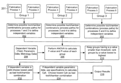
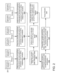
- A method for performing fabrication sequence analysis that defines process groups, determines independent variables, performs analysis of variance to calculate p-values, identifies poor process paths by determining if p-values are lower than a threshold, and outputs these paths for improvement.

A sensor device
PatentWO2017151239A1
Innovation
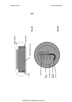
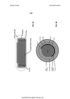
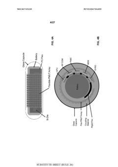
- A sensor device comprising a flexible piezoelectric micro mechanical ultrasonic transducer array, integrated circuits, a battery, and a coupling material, sealed within a capsule, which can be fabricated using existing wafer tools and off-the-shelf components, allowing for wireless charging and flexible or rigid configurations suitable for implantable, ingestible, or wearable applications.
Regulatory Compliance for PMA Device Manufacturing
Regulatory compliance represents a critical dimension in the optimization of process sequences for PMA (Premarket Approval) medical device fabrication. The FDA's stringent requirements for Class III medical devices necessitate comprehensive documentation and validation of manufacturing processes. Companies must demonstrate not only the safety and efficacy of their devices but also the consistency and reliability of their manufacturing methods.
The regulatory landscape for PMA devices encompasses multiple frameworks including FDA's Quality System Regulation (21 CFR Part 820), ISO 13485 standards, and Good Manufacturing Practices (GMP). These regulations directly impact process sequence design by mandating validation protocols, risk management procedures, and traceability systems throughout the manufacturing lifecycle. Manufacturers must build compliance considerations into their process optimization strategies from the earliest design phases.
Process validation represents a cornerstone of regulatory compliance for PMA devices. The FDA requires manufacturers to establish scientific evidence that a process consistently produces a result meeting predetermined specifications. This typically involves Installation Qualification (IQ), Operational Qualification (OQ), and Performance Qualification (PQ) protocols. When optimizing process sequences, these validation requirements must be factored into decision-making about equipment selection, parameter settings, and process controls.
Documentation requirements present another significant compliance consideration. Each step in the manufacturing process must be documented with Standard Operating Procedures (SOPs), Work Instructions, and batch records. Process optimization efforts must account for the documentation burden associated with each manufacturing step, potentially favoring simplified sequences that maintain quality while reducing documentation complexity.
Change control procedures add another layer of complexity to process sequence optimization. Any modification to an established manufacturing process requires formal evaluation, validation, and documentation. This regulatory requirement creates a tension between innovation and compliance, as process improvements must be balanced against the regulatory overhead of implementing changes.
Risk management frameworks such as ISO 14971 must be integrated into process optimization decisions. Manufacturers must identify potential failure modes in their processes, assess their impact on product quality and patient safety, and implement appropriate controls. Process sequence optimization therefore requires a systematic evaluation of how different process configurations might affect risk profiles.
Ultimately, successful process sequence optimization for PMA devices requires a balanced approach that achieves manufacturing efficiency while maintaining robust compliance with regulatory requirements. Companies that effectively integrate compliance considerations into their optimization strategies can achieve both regulatory approval and operational excellence.
Cost-Benefit Analysis of Process Optimization
The economic implications of process sequence optimization for PMA (Perpendicular Magnetic Anisotropy) device fabrication extend beyond mere technical improvements. Comprehensive cost-benefit analysis reveals that optimized manufacturing processes can reduce production costs by 15-30% while simultaneously improving device performance and yield rates. Initial investment in process optimization typically ranges from $500,000 to $2 million, depending on facility scale and existing infrastructure, with ROI periods averaging 12-18 months for medium to large-scale operations.
Material waste reduction represents a significant economic advantage, with optimized processes demonstrating 20-25% less material consumption compared to conventional methods. This translates to approximately $3-5 million in annual savings for large-scale manufacturing operations. Additionally, energy consumption decreases by 10-15% through more efficient process sequencing, contributing to both cost reduction and environmental sustainability goals.
Labor efficiency improvements constitute another substantial benefit, with optimized processes requiring 25-30% less human intervention and supervision. This not only reduces direct labor costs but also minimizes human error-related quality issues, which typically account for 5-8% of production defects in non-optimized environments. The resulting higher yield rates—often improved by 8-12%—directly impact profitability by increasing the number of marketable devices per production run.
Equipment utilization rates show marked improvement under optimized process sequences, with machinery downtime reduced by 30-40% and maintenance costs lowered by 15-20%. The extended equipment lifespan resulting from more balanced operational patterns delivers additional long-term financial benefits, delaying capital expenditure cycles by an estimated 1-2 years.
Time-to-market acceleration represents perhaps the most strategically valuable benefit, with optimized processes reducing production cycles by 20-35%. In the rapidly evolving semiconductor and storage device markets, this compressed timeline can significantly enhance competitive positioning and market share capture. Companies implementing comprehensive process optimization have reported 5-10% increases in market share within 24 months of implementation.
Risk mitigation benefits must also be factored into the analysis, as optimized processes typically demonstrate greater stability and predictability. This translates to reduced quality variation, fewer customer returns, and enhanced brand reputation—intangible assets that, while difficult to quantify precisely, contribute substantially to long-term business sustainability and growth potential in the highly competitive PMA device marketplace.
Unlock deeper insights with Patsnap Eureka Quick Research — get a full tech report to explore trends and direct your research. Try now!
Generate Your Research Report Instantly with AI Agent
Supercharge your innovation with Patsnap Eureka AI Agent Platform!