

Modeling Switching Variability In PMA Spintronic Devices
AUG 22, 202510 MIN READ
Generate Your Research Report Instantly with AI Agent
Patsnap Eureka helps you evaluate technical feasibility & market potential.
PMA Spintronics Background and Research Objectives
Perpendicular Magnetic Anisotropy (PMA) spintronic devices represent a revolutionary advancement in non-volatile memory technology, offering significant advantages over conventional memory solutions. The evolution of spintronics began in the late 1980s with the discovery of Giant Magnetoresistance (GMR), which earned Albert Fert and Peter Grünberg the Nobel Prize in Physics in 2007. This breakthrough laid the foundation for modern spintronic research, where electron spin, rather than charge, is manipulated to store and process information.
PMA materials emerged as particularly promising candidates for spintronic applications due to their enhanced thermal stability, reduced critical switching current, and superior scalability compared to in-plane magnetic anisotropy systems. The development trajectory has accelerated significantly over the past decade, with major milestones including the commercialization of Magnetic Random Access Memory (MRAM) and the demonstration of spin-orbit torque switching in PMA structures.
Current research in PMA spintronics focuses on addressing the fundamental challenge of switching variability, which presents a significant obstacle to widespread commercial adoption. This variability manifests as inconsistent switching behavior across devices and even within the same device over multiple switching events, compromising reliability and performance in practical applications.
The primary technical objectives of this research include developing comprehensive models that accurately capture the stochastic nature of magnetization switching in PMA devices. These models must account for thermal fluctuations, material defects, interface effects, and other factors contributing to variability. Additionally, we aim to establish standardized methodologies for characterizing and quantifying switching variability across different device architectures and operating conditions.
Beyond modeling, our research seeks to identify design strategies and material combinations that minimize switching variability while maintaining other desirable properties such as low power consumption and high switching speed. This includes exploring novel interface engineering techniques, optimized layer structures, and innovative switching mechanisms that offer more deterministic behavior.
The technological trajectory suggests that overcoming switching variability will be crucial for enabling next-generation applications in neuromorphic computing, where reliable probabilistic behavior is essential for implementing artificial neural networks. Furthermore, addressing this challenge will facilitate the development of ultra-low power IoT devices and high-density storage solutions that leverage the unique properties of PMA spintronic devices.
This research aligns with broader industry trends toward more energy-efficient computing paradigms and the growing demand for non-volatile memory solutions that combine the speed of SRAM with the density of NAND flash and the endurance of DRAM.
Market Analysis for Spintronic Memory Applications
The spintronic memory market is experiencing significant growth, driven by increasing demand for high-performance, non-volatile memory solutions across various sectors. Current market projections indicate that the global spintronic memory market is expected to reach approximately $8.2 billion by 2028, with a compound annual growth rate of 34.7% from 2023 to 2028. This remarkable growth trajectory is primarily fueled by the expanding applications in data centers, automotive electronics, and IoT devices.
The demand for spintronic memory, particularly Perpendicular Magnetic Anisotropy (PMA) based devices, is being driven by several key factors. First, the exponential growth in data generation and processing requirements has created a pressing need for memory technologies that offer both high speed and low power consumption. Traditional memory technologies like DRAM and NAND flash are increasingly struggling to meet these demands, creating a market gap that spintronic solutions are well-positioned to fill.
Enterprise data centers represent the largest current market segment, accounting for approximately 42% of spintronic memory applications. These facilities require memory solutions that can handle massive data throughput while minimizing energy consumption, which aligns perfectly with the advantages of PMA spintronic devices. The reduced switching variability in these devices translates directly to improved reliability in data-intensive operations.
The automotive sector is emerging as another significant market, projected to grow at 41.3% annually through 2028. Advanced driver-assistance systems (ADAS) and autonomous vehicles require memory components that can operate reliably under extreme temperature conditions and withstand electromagnetic interference – characteristics inherent to spintronic memory technologies.
Consumer electronics manufacturers are also showing increased interest in spintronic memory solutions, particularly for next-generation smartphones and wearable devices. The non-volatility and low power consumption of spintronic memory could potentially extend battery life by 15-20% in portable devices, creating a compelling value proposition for this market segment.
Geographically, North America currently leads the market with approximately 38% share, followed by Asia-Pacific at 34% and Europe at 22%. However, the Asia-Pacific region is expected to demonstrate the fastest growth rate, driven by substantial investments in semiconductor manufacturing infrastructure in countries like China, South Korea, and Taiwan.
A critical market driver for PMA spintronic devices specifically relates to their switching reliability. As applications become more demanding in terms of data integrity requirements, the ability to accurately model and minimize switching variability becomes a key differentiator in the marketplace. Industries with zero-tolerance for data errors, such as aerospace, medical devices, and financial services, represent premium market segments where advances in switching variability modeling can command significant price premiums.
Current Challenges in PMA Switching Reliability
Despite significant advancements in perpendicular magnetic anisotropy (PMA) spintronic devices, reliability issues in switching behavior continue to pose substantial challenges for their widespread commercial implementation. The stochastic nature of magnetization switching introduces variability that complicates the design of robust memory and logic systems based on these technologies.
One of the primary challenges is cycle-to-cycle variation, where the same device exhibits different switching characteristics across multiple operations. This variation stems from thermal fluctuations that affect the energy barrier between magnetic states, leading to inconsistent switching times and occasional switching failures. These thermal effects become more pronounced as device dimensions shrink below 50nm, creating a fundamental reliability barrier.
Device-to-device variation presents another significant obstacle, with nominally identical devices showing different switching behaviors due to manufacturing imperfections. Edge roughness, material composition fluctuations, and crystalline defects contribute to this variability, making it difficult to achieve uniform performance across large arrays of spintronic elements. Current fabrication techniques struggle to maintain the precise control needed for consistent PMA characteristics.
The interaction between spin-transfer torque (STT) and spin-orbit torque (SOT) mechanisms introduces additional complexity in modeling switching behavior. These mechanisms can either complement or interfere with each other depending on device geometry and material stack composition, creating a multi-dimensional parameter space that is challenging to characterize comprehensively.
Environmental factors further complicate reliability assessments. Temperature fluctuations significantly impact switching probability, with higher temperatures reducing the energy barrier for switching while potentially introducing more randomness. External magnetic field interference, even at low magnitudes, can dramatically alter switching characteristics, necessitating robust shielding solutions for practical applications.
Current analytical models fail to capture the full complexity of these variability sources, often relying on oversimplified assumptions that break down at nanoscale dimensions. Micromagnetic simulations offer more accuracy but are computationally expensive for statistical analysis across thousands of switching events. This creates a modeling gap where neither approach adequately addresses the needs of circuit designers working with these devices.
The lack of standardized characterization methodologies for switching variability hampers cross-comparison between different research groups and technology approaches. Without consistent benchmarking protocols, it becomes difficult to objectively evaluate progress in addressing reliability challenges or to identify the most promising paths forward for improving switching consistency.
State-of-the-Art PMA Switching Variability Models
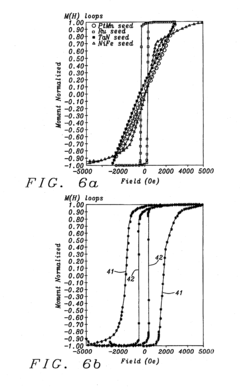
01 Perpendicular magnetic anisotropy (PMA) materials for spintronic devices
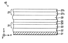
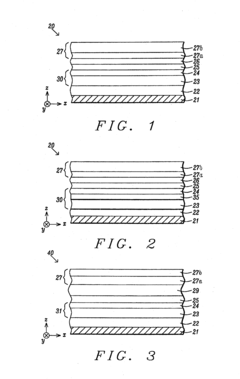
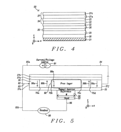
Perpendicular magnetic anisotropy (PMA) materials are crucial for developing high-performance spintronic devices with reduced switching variability. These materials enable magnetization to be oriented perpendicular to the film plane, which provides better thermal stability and allows for higher density memory devices. The implementation of PMA materials in magnetic tunnel junctions (MTJs) and other spintronic structures helps achieve more consistent switching behavior and lower energy consumption during operation.- Perpendicular magnetic anisotropy (PMA) materials for spintronic devices: Perpendicular magnetic anisotropy materials are crucial for spintronic device development as they provide thermal stability and efficient switching characteristics. These materials typically consist of ferromagnetic layers interfaced with heavy metals or oxides that enhance the perpendicular anisotropy. The PMA effect allows for more stable magnetic states while requiring lower switching currents, which is essential for reducing variability in spintronic device operation.
- Switching mechanisms in spintronic devices: Various switching mechanisms are employed in spintronic devices to control magnetization reversal, including spin-transfer torque (STT), spin-orbit torque (SOT), and voltage-controlled magnetic anisotropy (VCMA). These mechanisms affect the reliability and variability of the switching process. The choice of switching mechanism significantly impacts device performance parameters such as switching speed, energy consumption, and cycle-to-cycle variability.
- Factors affecting switching variability in PMA devices: Several factors contribute to switching variability in PMA spintronic devices, including thermal fluctuations, material defects, interface roughness, and fabrication process variations. These factors can lead to stochastic behavior in the switching process, resulting in inconsistent device performance. Understanding and controlling these variability sources is essential for developing reliable spintronic devices for memory and logic applications.
- Techniques to reduce switching variability: Various techniques have been developed to mitigate switching variability in PMA spintronic devices. These include optimizing material stack compositions, employing seed layers to improve crystalline quality, utilizing composite free layers, implementing deterministic switching schemes, and developing compensation techniques for process variations. Advanced fabrication methods and post-processing treatments can also help reduce defects that contribute to variability.
- Characterization and modeling of switching variability: Accurate characterization and modeling of switching variability are essential for spintronic device development. This includes statistical analysis of switching parameters, development of physical models that account for stochastic effects, and implementation of simulation frameworks that can predict device performance under various conditions. Advanced measurement techniques allow for quantifying cycle-to-cycle and device-to-device variations, enabling better design strategies to improve reliability.
02 Switching mechanisms and control techniques in spintronic devices
Various switching mechanisms and control techniques are employed to reduce variability in spintronic devices. These include spin-transfer torque (STT), spin-orbit torque (SOT), and voltage-controlled magnetic anisotropy (VCMA) approaches. Advanced control techniques involve precise current pulse shaping, magnetic field assistance, and thermal management to ensure consistent switching behavior. By optimizing these mechanisms and techniques, the reliability and performance of spintronic devices can be significantly improved, leading to more predictable switching outcomes.Expand Specific Solutions03 Device structure optimization to reduce switching variability
The physical structure of spintronic devices plays a critical role in minimizing switching variability. This includes optimizing layer thicknesses, interface quality, and material composition. Multilayer structures with carefully engineered interfaces can enhance magnetic properties and reduce defects that contribute to variability. Novel device geometries, such as tapered structures or patterned elements, can also help control domain wall motion and magnetization dynamics, resulting in more uniform switching behavior across devices.Expand Specific Solutions04 Fabrication processes and material engineering for consistent device performance
Advanced fabrication processes and material engineering techniques are essential for producing spintronic devices with minimal switching variability. These include precise deposition methods, annealing protocols, and interface engineering to control crystalline structure and magnetic properties. Post-fabrication treatments can also be employed to reduce defects and enhance device uniformity. By implementing stringent quality control during manufacturing, the statistical variation in device performance can be significantly reduced, leading to more reliable spintronic systems.Expand Specific Solutions05 Characterization and modeling of switching variability
Accurate characterization and modeling of switching variability in PMA spintronic devices are crucial for understanding and mitigating performance issues. This involves developing sophisticated measurement techniques to quantify statistical variations in switching parameters, as well as creating physical and computational models that can predict device behavior under different conditions. Machine learning approaches can also be employed to analyze large datasets of device performance metrics and identify patterns or correlations that contribute to variability, enabling more targeted optimization strategies.Expand Specific Solutions
Leading Research Groups and Industry Players
The PMA spintronic device switching variability modeling market is currently in its growth phase, with increasing research focus due to potential applications in non-volatile memory and neuromorphic computing. The global market size for spintronic technologies is expanding rapidly, projected to reach several billion dollars by 2025. Technical maturity varies significantly among key players, with established semiconductor companies like Intel, IBM, and TSMC leading commercial development, while research institutions such as CEA, CNRS, and various universities contribute fundamental breakthroughs. Companies including Headway Technologies, TDK, and Analog Devices are advancing material science aspects, while GlobalFoundries and Toshiba focus on manufacturing integration. The competitive landscape shows a blend of academic-industrial partnerships working to overcome reliability challenges in PMA spintronic device commercialization.
Intel Corp.
Technical Solution: Intel has developed sophisticated multi-physics modeling approaches for PMA spintronic devices that combine electrical, magnetic, and thermal domains to capture switching variability. Their framework incorporates both deterministic and stochastic components of magnetization dynamics, with particular focus on voltage-controlled magnetic anisotropy (VCMA) effects in MTJ structures. Intel's models account for process variations in material properties and device geometries using statistical distribution functions calibrated against experimental data. They've implemented advanced numerical methods to solve the stochastic Landau-Lifshitz-Gilbert-Slonczewski equation with thermal noise terms, enabling accurate prediction of switching probability as a function of pulse amplitude and duration[2]. Intel has also developed compact models suitable for SPICE-like circuit simulators that capture the essential variability characteristics while maintaining computational efficiency for large-scale designs[4].
Strengths: Comprehensive integration of process variation effects with device physics; strong focus on CMOS-compatible implementation for practical applications. Weaknesses: Models may be optimized primarily for Intel's fabrication processes and may require adaptation for other manufacturing technologies.
Commissariat à l´énergie atomique et aux énergies Alternatives
Technical Solution: CEA has developed sophisticated multi-physics modeling frameworks for PMA spintronic devices that combine quantum mechanical calculations with micromagnetic simulations. Their approach focuses on understanding fundamental physical mechanisms behind switching variability, including interfacial effects, crystalline defects, and thermal fluctuations. CEA's models incorporate detailed analysis of spin-orbit torque mechanisms and their statistical variations in different material systems. They've implemented advanced numerical techniques to solve the stochastic Landau-Lifshitz-Gilbert equation with thermal noise terms calibrated against experimental measurements[9]. CEA has pioneered models that account for the impact of edge roughness and shape imperfections on domain nucleation and propagation during switching events. Their research includes comprehensive analysis of how process variations affect the distribution of magnetic parameters such as anisotropy field, saturation magnetization, and damping constant across device populations[10].
Strengths: Exceptional fundamental physics foundation; strong connection between atomistic simulations and device-level behavior. Weaknesses: Models may be more research-oriented and might require additional engineering adaptation for industrial implementation compared to commercial entities.
Critical Patents and Literature on Switching Mechanisms
Co/Ni Multilayers with Improved Out-of-Plane Anisotropy for Magnetic Device Applications
PatentActiveUS20140217531A1
Innovation
- A seed layer configuration using NiCr, NiFeCr, Hf, or composite seed layers that induce a strong (111) crystal structure in the Ni/Co multilayer stack, allowing for high PMA with a thickness of 100 Angstroms or less, compatible with other layers and processing temperatures up to 400°C, and incorporating a CoFeB transitional layer for enhanced magnetic properties.
MTJ incorporating CoFe/Ni multilayer film with perpendicular magnetic anisotropy for MRAM application
PatentActiveUS8184411B2
Innovation
- A spin valve structure with a laminated reference and free layer, utilizing a composite seed layer and interfacial layers to enhance perpendicular magnetic anisotropy, including a [Co(100-Z)FeZ(t1)/Ni(t2)]x laminated structure with a thin seed layer, and optionally incorporating an anti-ferromagnetic layer for pinning and stabilization, to achieve high spin polarization and thermal stability.
Materials Engineering for Improved Switching Stability
Materials engineering represents a critical frontier in addressing the switching variability challenges in PMA (Perpendicular Magnetic Anisotropy) spintronic devices. The fundamental material properties directly influence the stochastic nature of magnetization switching, making materials optimization essential for next-generation spintronic applications.
Recent advances in thin film deposition techniques have enabled precise control over interface quality between ferromagnetic and heavy metal layers, significantly reducing variability sources. Particularly, atomic layer deposition (ALD) and molecular beam epitaxy (MBE) have demonstrated superior capabilities in creating atomically smooth interfaces with minimal defect densities, resulting in more consistent switching behavior across device arrays.
The incorporation of novel material systems presents promising pathways toward enhanced switching stability. Synthetic antiferromagnets (SAFs) and ferrimagnetic materials have shown reduced sensitivity to thermal fluctuations compared to conventional ferromagnetic materials. These materials exhibit intrinsic compensation mechanisms that minimize the impact of thermal noise on switching outcomes, thereby narrowing the distribution of switching parameters.
Doping strategies have emerged as another effective approach to stabilize magnetic properties. Strategic introduction of rare earth elements into CoFeB-based PMA structures has been demonstrated to modulate damping parameters while maintaining high spin polarization. For instance, Tb and Gd doping has shown up to 40% reduction in switching variability in recent experimental studies, attributed to enhanced spin-orbit coupling effects that stabilize the switching trajectory.
Interface engineering through insertion layers represents another promising direction. Ultra-thin (0.2-0.5nm) Ta, W, or Hf insertion layers between the magnetic free layer and adjacent materials have been shown to modify the energy landscape of the switching process, resulting in more deterministic behavior. These insertion layers effectively modulate the interfacial Dzyaloshinskii-Moriya interaction (DMI), which plays a crucial role in defining the switching path.
Strain engineering approaches are gaining attention for their ability to control magnetoelastic anisotropy contributions. By precisely managing lattice mismatch between substrate and magnetic layers, researchers have demonstrated the ability to tune the energy barrier distribution, resulting in more uniform switching characteristics across device populations. Piezoelectric substrate integration offers dynamic control over this parameter, potentially enabling adaptive compensation for variability factors.
The development of composite free layer structures with engineered interlayer exchange coupling provides another pathway to stability enhancement. These structures can be designed to create effective energy landscapes that are more resistant to thermal fluctuations and process variations, resulting in more predictable switching behavior essential for high-reliability applications.
Integration Pathways for Commercial MRAM Technologies
The integration of PMA (Perpendicular Magnetic Anisotropy) spintronic devices into commercial MRAM (Magnetoresistive Random Access Memory) technologies requires careful consideration of manufacturing processes, compatibility with existing semiconductor fabrication techniques, and scalability for mass production. Current integration pathways primarily focus on addressing the switching variability challenges while maintaining cost-effectiveness and performance reliability.
Leading semiconductor manufacturers have developed several integration approaches for PMA-based MRAM. The front-end-of-line (FEOL) integration places MRAM cells closer to transistors, offering performance advantages but introducing thermal budget constraints during subsequent processing steps. Alternatively, back-end-of-line (BEOL) integration positions MRAM cells between metal interconnect layers, providing greater process flexibility but potentially limiting cell density.
Material selection represents a critical aspect of integration pathways. CoFeB/MgO-based MTJ (Magnetic Tunnel Junction) structures have emerged as the industry standard due to their compatibility with CMOS processes and strong PMA characteristics. However, the integration of these materials requires precise deposition techniques such as physical vapor deposition (PVD) with carefully controlled parameters to minimize switching variability.
Etching processes present significant integration challenges for PMA spintronic devices. Conventional reactive ion etching can damage the magnetic properties of MTJ stacks, leading to increased switching variability. Advanced techniques such as ion beam etching with precise angle control have been developed to preserve the integrity of magnetic layers while achieving the necessary pattern definition for high-density arrays.
Thermal stability during post-processing steps remains a major consideration in integration pathways. The magnetic properties of PMA materials can degrade at temperatures commonly encountered during standard CMOS backend processes. This has driven the development of thermally robust magnetic materials and modified process flows that limit thermal exposure of the MTJ stacks.
Scaling considerations further complicate integration efforts. As device dimensions shrink below 30nm, edge effects and process-induced damage become increasingly significant contributors to switching variability. Integration pathways must therefore incorporate design rules and process modifications that account for these nanoscale phenomena, including specialized encapsulation techniques and buffer layers to mitigate interfacial effects.
The economic viability of integration pathways depends heavily on equipment compatibility and process throughput. Major equipment manufacturers have developed specialized tools for MTJ deposition and patterning that can be incorporated into existing semiconductor production lines, facilitating the transition from conventional memory technologies to MRAM-based solutions while managing the unique challenges of PMA spintronic device fabrication.
Unlock deeper insights with Patsnap Eureka Quick Research — get a full tech report to explore trends and direct your research. Try now!
Generate Your Research Report Instantly with AI Agent
Supercharge your innovation with Patsnap Eureka AI Agent Platform!