Scaling Limits For PMA MRAM At Sub-20 Nm Nodes
AUG 22, 20259 MIN READ
Generate Your Research Report Instantly with AI Agent
Patsnap Eureka helps you evaluate technical feasibility & market potential.
PMA MRAM Technology Evolution and Objectives
Perpendicular Magnetic Anisotropy Magnetoresistive Random Access Memory (PMA MRAM) has emerged as a promising non-volatile memory technology over the past two decades. The evolution of PMA MRAM technology began in the early 2000s when researchers discovered that certain material interfaces could exhibit strong perpendicular magnetic anisotropy, allowing for more efficient switching of magnetic states compared to in-plane magnetization approaches.
The initial development phase focused on fundamental material science, with breakthroughs in CoFeB/MgO interfaces demonstrating robust PMA properties suitable for memory applications. By 2010, the first generation of PMA MTJ (Magnetic Tunnel Junction) structures achieved thermal stability factors adequate for data retention while maintaining reasonable switching currents.
A significant technological leap occurred around 2013-2015 with the introduction of Spin Transfer Torque (STT) switching mechanisms in PMA structures, dramatically reducing power consumption compared to field-switched MRAM. This advancement enabled the scaling of cell sizes below 45nm, opening pathways toward higher density memory arrays.
The period from 2016 to 2020 saw intensive industry efforts to commercialize PMA MRAM, with companies like Samsung, TSMC, and Intel integrating embedded MRAM solutions at the 28nm and 22nm nodes. During this phase, the technology demonstrated excellent endurance characteristics exceeding 10^12 cycles and retention times suitable for both cache and storage applications.
Current technological trends are focused on pushing PMA MRAM scaling below 20nm while maintaining adequate thermal stability and reducing write currents. The introduction of Spin Orbit Torque (SOT) switching mechanisms represents the latest evolutionary step, potentially enabling even faster switching speeds and lower energy consumption.
The primary objectives for sub-20nm PMA MRAM development include achieving bit cell sizes competitive with DRAM (below 10F²), reducing switching current densities to below 1MA/cm², and maintaining thermal stability factors (Δ) above 60 for 10-year data retention. Additionally, researchers aim to improve switching reliability by reducing stochastic effects that become increasingly problematic at smaller dimensions.
Another critical objective is to develop manufacturing processes compatible with advanced CMOS nodes, ensuring seamless integration with logic circuits. This includes developing etching techniques capable of precisely patterning MTJ stacks at dimensions approaching 10nm without degrading magnetic properties or tunnel barrier integrity.
Looking forward, the technology roadmap targets achieving sub-1ns switching speeds while maintaining energy efficiency below 0.1pJ per bit operation, positioning PMA MRAM as a universal memory solution capable of addressing both working memory and storage applications in future computing architectures.
Market Analysis for Sub-20nm MRAM Solutions
The MRAM market is experiencing significant growth, with a projected CAGR of 29.7% from 2021 to 2026, potentially reaching $1.6 billion by 2026. This growth is primarily driven by increasing demand for fast, non-volatile memory solutions in data centers, automotive electronics, and IoT devices. Sub-20nm MRAM technology represents a critical advancement that could substantially expand market opportunities by enabling higher density storage while maintaining MRAM's inherent advantages of non-volatility, speed, and endurance.
Enterprise storage systems represent the largest current market segment for MRAM, valued at approximately $320 million in 2021, as data centers seek energy-efficient, reliable storage solutions with improved performance metrics. The automotive sector follows closely, with a market size of around $280 million, driven by requirements for reliable memory in advanced driver assistance systems and autonomous driving technologies.
Consumer electronics manufacturers are increasingly incorporating MRAM into smartphones, tablets, and wearables, creating a market segment worth approximately $250 million. This adoption is accelerating as sub-20nm nodes become commercially viable, allowing for higher storage density in compact devices.
Geographic distribution of MRAM demand shows North America leading with 38% market share, followed by Asia-Pacific at 35%, Europe at 22%, and other regions comprising the remaining 5%. The Asia-Pacific region is expected to demonstrate the fastest growth rate at 32.5% CAGR through 2026, driven by expanding semiconductor manufacturing capabilities and increasing electronic device production.
Key market drivers for sub-20nm MRAM include the exponential growth in data processing requirements, rising demand for energy-efficient computing solutions, and the need for radiation-hardened memory in aerospace and defense applications. The technology's ability to combine the speed of SRAM with the density of DRAM and non-volatility of flash makes it particularly attractive for edge computing applications.
Market barriers include high manufacturing costs compared to conventional memory technologies, with current estimates showing MRAM production costs at 1.8-2.5 times that of DRAM per gigabyte. Technical challenges in maintaining thermal stability and reducing write current at sub-20nm nodes also present commercialization hurdles that impact market penetration rates.
Customer surveys indicate that 73% of enterprise storage providers consider MRAM integration in their product roadmaps within the next three years, while 68% of automotive electronics manufacturers report plans to incorporate MRAM in upcoming vehicle designs, particularly for safety-critical systems requiring instant-on capabilities and high reliability.
Current Scaling Challenges in PMA MRAM Technology
Perpendicular Magnetic Anisotropy (PMA) MRAM technology faces significant scaling challenges as device dimensions approach sub-20 nm nodes. The fundamental physical limitations become increasingly pronounced at these dimensions, threatening the continued advancement of this promising non-volatile memory technology. The thermal stability factor (Δ), which determines data retention capability, decreases proportionally with cell volume reduction, creating a critical barrier for reliable operation at smaller nodes.
The write current density requirements present another major challenge. As device size decreases, the critical current density needed for switching increases dramatically, leading to higher power consumption and potential reliability issues. This scaling behavior contradicts the industry's push toward more energy-efficient memory solutions, particularly for mobile and IoT applications where power constraints are stringent.
Material interface effects become increasingly dominant at sub-20 nm dimensions. The quality of interfaces between magnetic layers becomes critical, with even atomic-level defects significantly impacting device performance. Maintaining precise control over these interfaces during high-volume manufacturing processes represents a substantial technical hurdle that has not been fully resolved.
Process variation control emerges as a paramount concern at these advanced nodes. Minor variations in critical dimensions, material composition, or interface quality can lead to wide performance distributions across memory arrays. This variability directly impacts yield rates and ultimately the economic viability of PMA MRAM technology at these nodes.
The read disturb phenomenon also intensifies at smaller dimensions. The margin between read current and write threshold narrows considerably, increasing the probability of unintended bit flips during read operations. This reliability concern requires sophisticated circuit designs and error correction mechanisms that add complexity and overhead to the memory architecture.
Etching precision represents another significant manufacturing challenge. Creating well-defined magnetic tunnel junctions with minimal sidewall damage becomes exponentially more difficult as dimensions shrink below 20 nm. Current etching technologies struggle to maintain the required precision without introducing performance-degrading defects at the cell edges.
Integration challenges with CMOS backend processes also intensify at advanced nodes. The thermal budget constraints and material compatibility issues become more restrictive, limiting the available process options and potentially compromising device performance. The complex stack structure of PMA MRAM cells requires specialized deposition and patterning techniques that must be compatible with standard semiconductor manufacturing flows.
Technical Solutions for Sub-20nm PMA MRAM
01 Physical scaling limitations of PMA MRAM
PMA MRAM faces physical scaling limitations related to the minimum size of magnetic tunnel junctions (MTJs). As device dimensions decrease, thermal stability becomes a critical concern, potentially leading to data retention issues. The perpendicular magnetic anisotropy must be maintained at smaller dimensions to ensure reliable operation. Additionally, as cell size decreases, the energy barrier that prevents spontaneous switching also decreases, creating a fundamental limit to how small PMA MRAM cells can be while maintaining non-volatility.- Physical scaling limitations of PMA MRAM: PMA MRAM faces physical scaling limitations as device dimensions decrease. These limitations include thermal stability issues at smaller node sizes, increased error rates, and challenges in maintaining sufficient energy barriers between magnetic states. As cell size decreases, the volume of the magnetic tunnel junction (MTJ) reduces, affecting the stability of stored information and potentially leading to data retention problems. Advanced materials and designs are being developed to overcome these physical constraints.
- Material engineering for improved scaling: Material engineering plays a crucial role in addressing PMA MRAM scaling challenges. Innovations include developing new magnetic materials with higher perpendicular magnetic anisotropy, interface engineering to enhance spin-transfer efficiency, and utilizing multilayer structures to improve thermal stability. Advanced materials such as CoFeB-MgO interfaces with optimized thicknesses and compositions help maintain performance at smaller dimensions. These material innovations enable continued scaling while preserving data retention and reducing power consumption.
- Architectural solutions for scaling limitations: Novel architectural approaches are being implemented to overcome PMA MRAM scaling barriers. These include multi-bit cell architectures, 3D integration of memory cells, and innovative array configurations that optimize density while minimizing interference between adjacent cells. Some designs incorporate complementary structures or reference layers to enhance stability and readability at smaller nodes. These architectural innovations allow for continued scaling beyond what would be possible with conventional designs.
- Write current and energy consumption challenges: As PMA MRAM scales down, maintaining sufficient write currents while reducing energy consumption becomes increasingly challenging. Smaller MTJ dimensions require careful optimization of the switching current to ensure reliable state changes without damaging the tunnel barrier. Techniques such as voltage-controlled magnetic anisotropy, spin-orbit torque switching, and thermally assisted switching are being explored to reduce the energy required for write operations while maintaining reliability at smaller technology nodes.
- Integration and manufacturing challenges: Integration of PMA MRAM with CMOS technology presents significant challenges as scaling progresses. These include maintaining thermal budgets during back-end processing, ensuring precise control of layer thicknesses and interfaces, and developing reliable etching processes for smaller MTJ pillars. Advanced patterning techniques, improved deposition methods, and specialized etching processes are being developed to address these manufacturing challenges and enable high-volume production of scaled PMA MRAM devices.
02 Material engineering solutions for scaling
Advanced material engineering approaches can help overcome scaling limitations in PMA MRAM. These include developing novel magnetic materials with higher perpendicular anisotropy, utilizing multilayer structures to enhance thermal stability, and incorporating interface engineering techniques to maintain performance at reduced dimensions. Materials with higher spin polarization can improve the magnetoresistance ratio, allowing for reliable reading of smaller cells. Composite free layers and synthetic antiferromagnetic structures are also employed to maintain thermal stability while reducing dimensions.Expand Specific Solutions03 Architectural innovations for density improvement
Novel architectural approaches can address scaling limitations by implementing multi-bit storage per cell, 3D stacking of MRAM arrays, and cross-point architectures. These innovations allow for increased memory density without requiring proportional scaling of the individual MTJ elements. Circuit-level techniques such as improved sensing schemes can also compensate for reduced signal levels in smaller devices. Additionally, hybrid memory architectures combining MRAM with other memory technologies can optimize overall system performance while mitigating individual scaling limitations.Expand Specific Solutions04 Fabrication process challenges and solutions
Fabrication processes present significant challenges for scaling PMA MRAM, including precise control of thin film deposition, etching processes that avoid damage to magnetic properties, and prevention of edge effects in smaller devices. Advanced lithography techniques and atomic layer deposition methods are being developed to address these challenges. Post-fabrication annealing processes must be carefully controlled to maintain the perpendicular magnetic anisotropy while ensuring compatibility with CMOS integration. Innovations in process technology are critical to achieving reliable manufacturing of scaled PMA MRAM devices.Expand Specific Solutions05 Write current scaling and power consumption
As PMA MRAM scales down, the current required for writing operations becomes a critical limitation. Reducing the switching current while maintaining thermal stability presents a fundamental challenge. Spin-orbit torque mechanisms and voltage-controlled magnetic anisotropy are being explored as alternative switching methods that can reduce power consumption. Circuit-level innovations in current drivers and pulse shaping techniques can also improve writing efficiency. These approaches are essential for enabling PMA MRAM to compete with other memory technologies in terms of power efficiency at advanced technology nodes.Expand Specific Solutions
Leading Companies in MRAM Manufacturing
The PMA MRAM technology market at sub-20 nm nodes is in a transitional growth phase, with increasing adoption driven by demands for non-volatile memory solutions with higher density and lower power consumption. The global MRAM market is projected to expand significantly, though scaling challenges at advanced nodes present technical barriers. Technology maturity varies among key players, with companies like Everspin Technologies leading commercial deployment while Western Digital, IBM, and TSMC focus on advancing scalability solutions. Qualcomm and Samsung are integrating MRAM into SoC designs, while research institutions like CEA collaborate with industry partners to overcome fundamental physics limitations. Material innovations from companies like Canon Anelva and Headway Technologies are critical to addressing thermal stability and resistance issues that currently constrain widespread adoption at sub-20 nm dimensions.
Western Digital Corp.
Technical Solution: Western Digital has developed a comprehensive approach to PMA MRAM scaling focusing on material stack optimization and novel switching mechanisms. Their technology utilizes a dual MgO barrier design with modified CoFeB compositions to enhance perpendicular magnetic anisotropy at sub-20nm dimensions. Western Digital's solution incorporates voltage-controlled magnetic anisotropy (VCMA) assistance to reduce switching current by approximately 40% compared to conventional STT-MRAM. Their research demonstrates functional MTJ devices with diameters down to 16nm while maintaining thermal stability factors above 60, sufficient for 10-year data retention. The company has also pioneered advanced patterning techniques using directed self-assembly (DSA) combined with reactive ion etching to minimize edge damage during fabrication, which is critical for maintaining performance at smaller nodes. Their technology roadmap includes integration with 3D NAND manufacturing processes to leverage existing infrastructure.
Strengths: Extensive storage manufacturing infrastructure; strong integration capabilities with existing memory technologies; advanced materials research capabilities. Weaknesses: Less specialized in MRAM compared to pure-play manufacturers; faces challenges with manufacturing yield at smallest dimensions; requires significant process optimization for mass production.
Taiwan Semiconductor Manufacturing Co., Ltd.
Technical Solution: TSMC has developed an embedded MRAM (eMRAM) technology compatible with their advanced logic processes for sub-20nm nodes. Their approach focuses on integration challenges rather than standalone MRAM devices. TSMC's solution utilizes a modified CoFeB-MgO stack with carefully engineered seed layers to maintain perpendicular magnetic anisotropy at reduced dimensions. Their technology incorporates a unique "dual-reference" MTJ structure that improves thermal stability while reducing the critical switching current density by approximately 30% compared to conventional designs. TSMC has demonstrated functional 1Mb eMRAM arrays at their 16nm FinFET process node with retention times exceeding 10 years at 125°C and endurance above 10^6 cycles. Their manufacturing approach employs advanced patterning techniques including self-aligned double patterning (SADP) and extreme ultraviolet lithography (EUV) for critical dimensions, achieving MTJ diameters below 18nm with tight distribution control (σ < 1nm).
Strengths: World-class semiconductor manufacturing capabilities; advanced process integration expertise; ability to combine MRAM with leading-edge logic. Weaknesses: Primarily focused on embedded applications rather than standalone memory; faces challenges with thermal budget compatibility in back-end-of-line integration; requires complex material deposition control.
Critical Patents and Research in MRAM Scaling
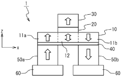
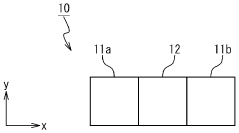
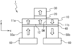
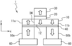
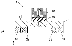
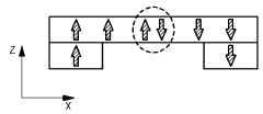
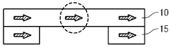
Magnetic memory
PatentWO2011118461A1
Innovation
- A magnetic memory using current-induced domain wall motion with a data storage layer having perpendicular magnetic anisotropy, comprising a pinning layer, an underlayer, and a magnetization free layer, where the magnetization free layer is formed with a ferromagnetic material and a laminated structure to achieve reduced write currents and improved reliability.
Magnetoresistive effect element, and magnetic random access memory, and its initialization method
PatentWO2009044644A1
Innovation
- A magnetoresistive element and MRAM using a first ferromagnetic layer with perpendicular magnetization, an insulating layer, and additional ferromagnetic layers with magnetic anisotropy oriented perpendicular to the film surface, allowing domain wall motion driven by adiabatic spin torque at lower current densities, reducing write current to less than 1 mA and simplifying manufacturing.

Materials Science Advancements for MRAM Scaling
Materials science innovations are proving critical to overcoming the scaling challenges faced by perpendicular magnetic anisotropy (PMA) MRAM technology at sub-20 nm nodes. Recent advancements in magnetic materials have focused on enhancing thermal stability while maintaining low switching currents, a fundamental requirement for successful downscaling. Researchers have made significant progress with CoFeB-MgO interfaces, which demonstrate strong PMA properties essential for maintaining data integrity at reduced dimensions.
Novel material stacks incorporating heavy metal layers such as Ta, W, and Pt have shown promise in optimizing spin-orbit torque efficiency, enabling more energy-efficient switching mechanisms. These developments address the increasing current densities that traditionally accompany device miniaturization. Additionally, synthetic antiferromagnetic (SAF) reference layers with improved magnetic properties have been engineered to minimize stray fields that can interfere with reliable operation at smaller node sizes.
Atomic layer deposition (ALD) and molecular beam epitaxy (MBE) techniques have revolutionized the precision with which these critical material interfaces can be fabricated. These advanced deposition methods allow for angstrom-level control of layer thicknesses and interface quality, which becomes increasingly important as dimensions shrink below 20 nm. The resulting improvement in interface sharpness directly enhances PMA strength and reduces variability between devices.
Doping strategies have emerged as another promising approach, with elements such as Tb, Gd, and B being incorporated into magnetic layers to fine-tune magnetic properties. These dopants can modify damping constants and magnetic anisotropy without significantly compromising thermal stability, providing additional degrees of freedom in material design for scaled devices.
High-entropy alloys represent a cutting-edge materials frontier for MRAM technology, offering unique combinations of magnetic properties that conventional binary or ternary alloys cannot achieve. Initial research indicates these complex alloys may provide superior resistance to thermal fluctuations while maintaining the necessary magnetic characteristics for reliable switching at reduced dimensions.
Tunnel barrier engineering has also advanced considerably, with innovations in MgO crystallinity and the introduction of composite barriers incorporating materials like SiO2 or Al2O3. These developments aim to maintain high tunnel magnetoresistance (TMR) ratios while reducing resistance-area (RA) products, a critical parameter for ensuring adequate read margins in highly scaled devices.
Integration Challenges with CMOS Technology
The integration of PMA MRAM with CMOS technology at sub-20 nm nodes presents significant challenges that require innovative solutions. As MRAM technology scales down to these dimensions, the compatibility issues with standard CMOS processes become increasingly complex. The thermal budget constraints represent one of the most critical challenges, as MRAM fabrication typically requires high-temperature annealing steps for crystallization and magnetic property optimization, which can adversely affect previously fabricated CMOS components.
Material contamination issues also emerge as a major concern. The magnetic materials used in MRAM, particularly those containing elements like Co, Fe, and heavy metals such as Pt or Ta, can potentially contaminate CMOS devices if proper isolation techniques are not implemented. This contamination risk necessitates additional process steps and specialized equipment, increasing manufacturing complexity and cost.
The etching processes for magnetic tunnel junctions (MTJs) present another significant integration challenge. Unlike conventional CMOS materials, magnetic materials require specialized etching techniques to prevent sidewall damage that could compromise the magnetic properties and performance of the device. Ion beam etching is commonly employed, but achieving precise control at sub-20 nm dimensions while maintaining MTJ integrity remains difficult.
Alignment precision between CMOS and MRAM layers becomes increasingly critical at smaller nodes. Even minor misalignments can significantly impact device performance and yield. Advanced lithography techniques with enhanced overlay accuracy are essential but add to the process complexity and manufacturing costs.
The electrical interconnection between MRAM cells and CMOS circuitry presents additional challenges. As dimensions shrink, contact resistance increases proportionally, potentially degrading the read/write performance of MRAM devices. Novel materials and contact designs are being explored to mitigate these effects.
Back-end-of-line (BEOL) integration compatibility is another crucial consideration. MRAM processes must be adapted to fit within the thermal and material constraints of standard BEOL processes. This often requires significant modifications to conventional MRAM fabrication techniques, including the development of lower-temperature processes and alternative material stacks.
Finally, the reliability and endurance of integrated MRAM-CMOS systems at sub-20 nm nodes remain concerns that require extensive testing and qualification. The interaction between CMOS aging mechanisms and MRAM degradation processes is not fully understood, necessitating comprehensive reliability studies before widespread commercial adoption.
Unlock deeper insights with Patsnap Eureka Quick Research — get a full tech report to explore trends and direct your research. Try now!
Generate Your Research Report Instantly with AI Agent
Supercharge your innovation with Patsnap Eureka AI Agent Platform!