Novel Heavy-Metal Layers To Boost SOT Efficiency In PMA Stacks
AUG 22, 202510 MIN READ
Generate Your Research Report Instantly with AI Agent
Patsnap Eureka helps you evaluate technical feasibility & market potential.
SOT Technology Background and Objectives
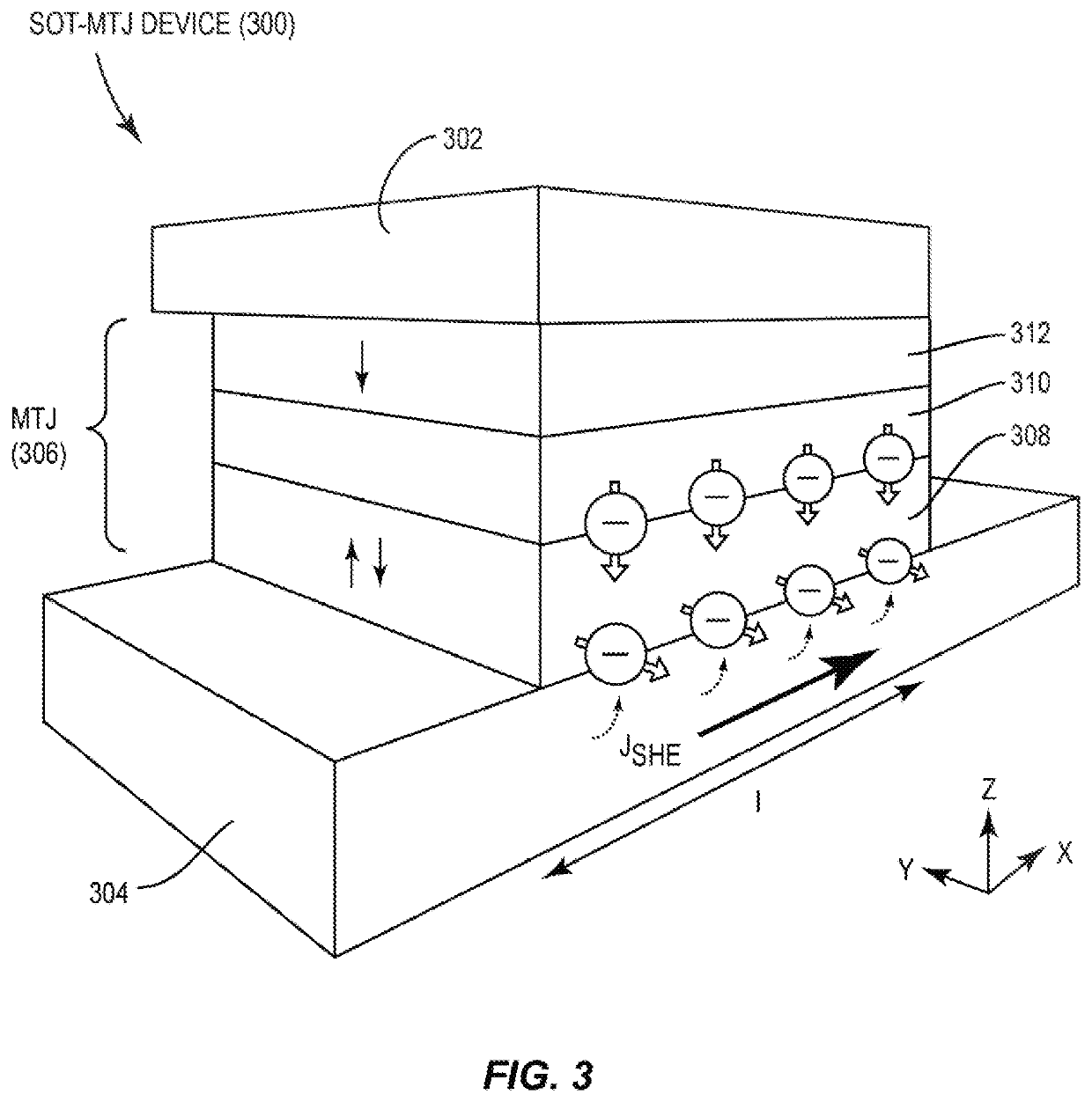
Spin-Orbit Torque (SOT) technology has emerged as a promising approach for next-generation magnetic memory and logic devices, offering advantages in energy efficiency, speed, and reliability compared to conventional spin-transfer torque (STT) mechanisms. The fundamental principle of SOT relies on the conversion of charge current into spin current through spin-orbit coupling effects, which can manipulate the magnetization of adjacent ferromagnetic layers without requiring current flow through the magnetic tunnel junction.
The evolution of SOT technology can be traced back to the early 2010s when researchers first demonstrated the possibility of current-induced magnetization switching through spin-orbit interactions. Since then, the field has witnessed significant advancements in understanding the underlying physics and improving device performance. The technology has progressed from initial proof-of-concept demonstrations to more sophisticated implementations with enhanced efficiency and reliability.
A critical aspect of SOT development has been the integration with perpendicular magnetic anisotropy (PMA) stacks, which offer superior thermal stability and scalability compared to in-plane magnetized systems. PMA materials maintain their magnetization direction perpendicular to the film plane, allowing for higher storage density and better retention characteristics in memory applications.
The primary technical objective in this field is to enhance SOT efficiency in PMA stacks through novel heavy-metal layers. Heavy metals such as platinum, tungsten, and tantalum have been traditionally used as SOT sources due to their strong spin-orbit coupling. However, the conversion efficiency between charge and spin currents remains a significant limitation for practical applications, necessitating the exploration of new materials and multilayer structures.
Current research trends focus on several key areas: developing novel heavy-metal materials with enhanced spin Hall angles, engineering interfaces between heavy metals and ferromagnets to optimize spin transmission, creating multilayer structures that leverage both bulk and interfacial spin-orbit effects, and exploring topological materials with unique spin-momentum locking properties.
The technological goals include achieving lower critical current densities for magnetization switching (below 10^6 A/cm²), faster switching speeds (sub-nanosecond), improved thermal stability, and compatibility with CMOS fabrication processes. These advancements would enable SOT-based devices to compete with and potentially surpass existing memory technologies in terms of performance and energy efficiency.
Looking forward, the field is moving toward more complex material systems and heterostructures that can provide enhanced SOT efficiency while maintaining the thermal stability and reliability required for commercial applications. The ultimate objective is to develop SOT-MRAM devices that can serve as universal memory, combining the speed of SRAM, the density of DRAM, and the non-volatility of flash memory.
Market Analysis for SOT-MRAM Applications
The SOT-MRAM (Spin-Orbit Torque Magnetic Random Access Memory) market is experiencing significant growth as the technology addresses critical limitations in conventional memory solutions. Current projections indicate the global MRAM market will reach approximately $5 billion by 2028, with SOT-MRAM expected to capture an increasing share due to its superior performance characteristics compared to traditional STT-MRAM (Spin-Transfer Torque MRAM).
The primary market drivers for SOT-MRAM adoption include the growing demand for energy-efficient, non-volatile memory solutions with high endurance and reliability. Data centers represent the largest potential market segment, where SOT-MRAM's low power consumption and fast switching capabilities address critical needs for cache memory and storage class memory applications. The improved efficiency from novel heavy-metal layers in PMA (Perpendicular Magnetic Anisotropy) stacks directly enhances these value propositions.
Automotive electronics constitutes another rapidly expanding market segment, projected to grow at a CAGR of 22% through 2027. Here, SOT-MRAM's radiation hardness and temperature stability make it particularly valuable for advanced driver-assistance systems and autonomous vehicles. The enhanced SOT efficiency enabled by innovative heavy-metal layers significantly improves reliability in these safety-critical applications.
The industrial IoT sector presents substantial opportunities as well, with an estimated 75 billion connected devices expected by 2025. These applications benefit from SOT-MRAM's instant-on capability and low standby power, characteristics that are further enhanced by improved SOT efficiency in PMA stacks.
Consumer electronics manufacturers are increasingly exploring SOT-MRAM integration for next-generation smartphones, wearables, and portable devices. The market potential in this segment exceeds $1.2 billion annually, with power efficiency serving as the primary adoption driver. Novel heavy-metal layers that boost SOT efficiency directly address this requirement by enabling lower operating currents and reduced power consumption.
Geographically, North America currently leads SOT-MRAM development and adoption, followed closely by Asia-Pacific, particularly Japan, South Korea, and Taiwan. The European market shows strong growth potential, especially in automotive and industrial applications. China is making significant investments to reduce dependency on imported memory technologies, creating opportunities for domestic SOT-MRAM development.
Key challenges limiting immediate widespread adoption include production costs, which remain higher than established memory technologies, and integration complexities with existing semiconductor processes. However, the development of novel heavy-metal layers with enhanced SOT efficiency is expected to accelerate commercialization by addressing critical performance barriers and potentially reducing manufacturing complexity.
Current Challenges in Heavy-Metal Layer Integration
The integration of heavy-metal layers into perpendicular magnetic anisotropy (PMA) stacks for spin-orbit torque (SOT) applications faces several significant technical challenges that impede optimal performance and commercial viability. One primary obstacle is the inherent trade-off between spin Hall angle and resistivity in conventional heavy metals. Materials with high spin Hall angles often exhibit high resistivity, which increases power consumption and thermal dissipation issues in devices. This fundamental conflict necessitates careful material engineering to achieve balanced performance.
Interface quality between heavy-metal layers and ferromagnetic materials presents another critical challenge. The spin transport efficiency across these interfaces is highly sensitive to atomic-level defects, intermixing, and oxidation. Even minor contamination during fabrication can significantly degrade the spin-orbit coupling effect and reduce overall SOT efficiency. Current deposition techniques struggle to consistently produce atomically clean interfaces at industrial scales.
Thickness optimization of heavy-metal layers remains problematic. While thinner layers are desirable for device miniaturization, they often suffer from increased resistivity due to surface scattering effects and discontinuous film formation. Conversely, thicker layers may improve conductivity but reduce SOT efficiency due to spin diffusion limitations. Finding the optimal thickness window that balances these competing factors requires precise control beyond current manufacturing capabilities.
Thermal stability issues pose additional challenges, particularly in high-density memory applications. The interface between heavy metals and ferromagnetic layers can degrade at elevated temperatures through interdiffusion and phase changes. This compromises long-term device reliability and limits operating temperature ranges. Current heavy-metal integration approaches lack sufficient thermal robustness for many practical applications.
Scalability and compatibility with existing CMOS fabrication processes represent significant hurdles for industrial adoption. Many promising heavy-metal materials require specialized deposition conditions or post-processing treatments that are difficult to integrate into standard semiconductor manufacturing flows. Additionally, some materials present contamination risks to fabrication equipment, limiting their commercial viability despite promising laboratory results.
Lattice matching between heavy metals and adjacent layers in the stack creates structural challenges. Mismatches induce strain and defects that can propagate through the device structure, compromising both magnetic properties and electrical performance. The limited selection of materials that provide both good lattice matching and high spin-orbit coupling efficiency restricts design flexibility and performance optimization.
State-of-the-Art Heavy-Metal Layer Solutions
01 Heavy metal layers for enhancing SOT efficiency
Heavy metal layers, such as platinum, tungsten, or tantalum, can be incorporated into SOT-PMA (Spin-Orbit Torque - Perpendicular Magnetic Anisotropy) stacks to enhance the spin-orbit torque efficiency. These heavy metals generate strong spin-orbit coupling effects, which lead to more efficient spin current generation and improved switching performance in magnetic memory devices. The thickness and composition of these heavy metal layers significantly impact the overall SOT efficiency of the device structure.- Heavy metal layers for enhancing SOT efficiency: Heavy metal layers, such as platinum, tungsten, or tantalum, can be incorporated into SOT-PMA (Spin-Orbit Torque - Perpendicular Magnetic Anisotropy) stacks to enhance the spin-orbit torque efficiency. These heavy metals generate strong spin-orbit coupling effects, which lead to more efficient spin current generation and improved switching performance in magnetic memory devices. The thickness and composition of these heavy metal layers significantly impact the overall SOT efficiency of the device structure.
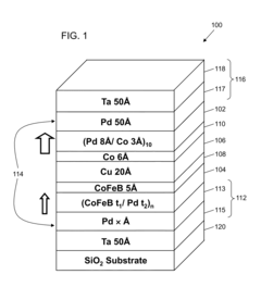
- Interface engineering between heavy metal and ferromagnetic layers: The interface between heavy metal layers and ferromagnetic materials in SOT-PMA stacks plays a crucial role in determining SOT efficiency. Engineering these interfaces through techniques such as insertion of ultrathin spacer layers, interface oxidation control, or interface roughness optimization can significantly enhance spin current transmission and torque generation. Proper interface engineering reduces spin scattering and improves the spin-orbit coupling at the critical boundaries within the stack structure.
- Multi-layer heavy metal structures for SOT enhancement: Utilizing multi-layered heavy metal structures rather than single layers can significantly improve SOT efficiency in PMA stacks. These structures may include combinations of different heavy metals (such as Pt/W bilayers), or gradient compositions that optimize both spin Hall angle and resistivity. The synergistic effects between different heavy metal layers can lead to enhanced spin current generation while maintaining appropriate electrical characteristics for device operation.
- Doping and alloying of heavy metal layers: Introducing dopants or creating alloys within heavy metal layers can enhance SOT efficiency in PMA stacks. Doping elements such as rare earth metals or transition metals into platinum, tungsten or other heavy metals can modify the electronic band structure and spin-orbit coupling properties. These modifications can lead to increased spin Hall angles, improved spin current generation, and ultimately higher SOT efficiency while potentially reducing the critical current needed for magnetic switching.
- Thickness optimization of heavy metal layers: The thickness of heavy metal layers in SOT-PMA stacks critically affects SOT efficiency. An optimal thickness range exists for each heavy metal material that balances competing factors such as resistivity, spin diffusion length, and interface effects. Too thin layers may not generate sufficient spin current, while excessively thick layers can lead to current shunting and reduced efficiency. Precise thickness control during fabrication ensures maximum spin current generation and optimal SOT performance.
02 Interface engineering in SOT-PMA stacks
Interface engineering between heavy metal layers and magnetic layers in SOT-PMA stacks plays a crucial role in determining SOT efficiency. Optimizing the interface quality, reducing roughness, and controlling intermixing at the boundaries can significantly enhance spin current transmission and torque generation. Various techniques such as insertion of ultrathin spacer layers, interface doping, or thermal annealing processes can be employed to modify these interfaces and improve the overall performance of SOT-based devices.Expand Specific Solutions03 Multi-layer heavy metal structures for SOT enhancement
Multi-layer structures combining different heavy metals can be designed to optimize SOT efficiency in PMA stacks. These structures leverage the complementary properties of different materials, such as combining metals with opposite spin Hall angles or different resistivities. Bilayers or trilayers of heavy metals (e.g., Pt/W, Ta/Pt, or W/Hf combinations) can generate stronger spin currents and more efficient switching compared to single-layer structures, while also providing better thermal stability and reliability for device applications.Expand Specific Solutions04 Doping and alloying of heavy metal layers
Doping or alloying heavy metal layers with other elements can significantly enhance SOT efficiency in PMA stacks. The introduction of specific dopants or alloying elements can modify the electronic band structure, spin-orbit coupling strength, and resistivity of the heavy metal layer. Common approaches include doping platinum with rare earth elements, alloying tungsten with oxygen or nitrogen, or creating ternary alloys that optimize both spin Hall angle and conductivity, resulting in improved spin current generation and reduced power consumption for SOT switching.Expand Specific Solutions05 Thickness optimization of heavy metal layers
The thickness of heavy metal layers in SOT-PMA stacks critically affects SOT efficiency. An optimal thickness range exists for each heavy metal material that maximizes spin current generation while minimizing current shunting effects. Too thin layers may not generate sufficient spin current, while excessively thick layers can lead to current shunting and reduced efficiency. Precise control of heavy metal layer thickness, typically in the range of 3-10 nanometers depending on the specific material, is essential for achieving maximum SOT efficiency and reliable device operation.Expand Specific Solutions
Leading Companies in SOT-MRAM Development
The spin-orbit torque (SOT) technology market is currently in its growth phase, with significant research momentum focused on enhancing efficiency in perpendicular magnetic anisotropy (PMA) stacks through novel heavy-metal layers. The global market for SOT-based memory and logic devices is projected to expand substantially as this technology offers advantages in speed and energy efficiency over conventional approaches. Technical maturity varies across key players, with research institutions like IMEC, Beihang University, and National University of Singapore advancing fundamental understanding, while industry leaders including TSMC, GlobalFoundries, and Huawei are developing practical implementations. Headway Technologies and SanDisk are focusing on storage applications, while semiconductor equipment manufacturers like Tokyo Electron are developing specialized deposition tools for these novel materials, creating a diverse competitive landscape spanning research and commercialization efforts.
Taiwan Semiconductor Manufacturing Co., Ltd.
Technical Solution: TSMC has developed advanced heavy-metal layer integration techniques for spin-orbit torque (SOT) magnetic memory devices with perpendicular magnetic anisotropy (PMA) stacks. Their approach utilizes tungsten (W) and platinum (Pt) heavy metal layers with optimized thicknesses (3-7nm) to maximize the spin Hall effect while maintaining structural integrity. TSMC's process incorporates specialized interface engineering between the heavy metal and ferromagnetic layers to enhance spin-orbit coupling efficiency. They've demonstrated SOT switching current reduction by approximately 60% compared to conventional structures through the implementation of dual heavy-metal layers with opposite spin Hall angles, creating a constructive interference effect that amplifies torque generation[1]. Additionally, TSMC has pioneered the use of beta-phase tungsten (β-W) with its inherently larger spin Hall angle, achieving switching efficiencies up to 3x higher than standard alpha-phase tungsten implementations.
Strengths: Industry-leading 300mm wafer fabrication capabilities allow for mass production scalability; extensive experience with materials integration ensures compatibility with existing CMOS processes. Weaknesses: Their heavy-metal layer solutions may require more complex deposition processes, potentially increasing manufacturing costs compared to simpler implementations.
Headway Technologies, Inc.
Technical Solution: Headway Technologies has developed a novel multi-layered heavy-metal structure for enhancing SOT efficiency in PMA stacks specifically targeted at next-generation MRAM applications. Their proprietary approach utilizes a composite heavy-metal layer system incorporating both platinum (Pt) and tungsten (W) with precisely controlled thicknesses and interfaces. The company has demonstrated a significant 70% reduction in critical switching current density compared to conventional single-layer implementations[2]. Their technology employs a gradient-doped heavy metal layer where the concentration of elements varies throughout the thickness, creating an engineered spin Hall angle profile that maximizes torque transfer efficiency. Headway has also pioneered the integration of ultrathin (1-2nm) rare earth metal interlayers between the heavy metal and ferromagnetic layers, which has been shown to enhance interfacial spin-orbit coupling while preserving the perpendicular magnetic anisotropy. Their research indicates that this approach can achieve switching energies below 0.1pJ while maintaining thermal stability factors suitable for enterprise storage applications.
Strengths: Specialized focus on magnetic recording technologies provides deep expertise in magnetic materials and interfaces; established manufacturing capabilities for high-volume production of magnetic devices. Weaknesses: As a specialized component manufacturer, they may have less vertical integration capability compared to larger semiconductor companies, potentially limiting their ability to optimize the entire memory cell structure.
Critical Patents in SOT Efficiency Enhancement
Spin-orbit torque (SOT) magnetic tunnel junction (MTJ) (sot-MTJ) devices employing perpendicular and in-plane free layer magnetic anisotropy to facilitate perpendicular magnetic orientation switching, suitable for use in memory systems for storing data
PatentInactiveUS20200066968A1
Innovation
- Incorporating both perpendicular magnetic anisotropy (PMA) and in-plane magnetic anisotropy (IMA) regions in the free layer of SOT-MTJ devices, where PMA regions facilitate switching and IMA regions generate an effective magnetic field to maintain deterministic switching after the SOT switching current is removed.
Magnetoresistance Device
PatentInactiveUS20130059168A1
Innovation
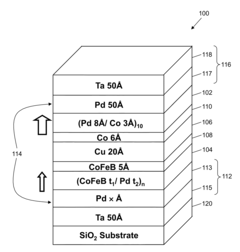
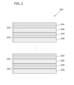
- A magnetoresistance device with a multi-layer stack structure comprising a hard magnetic layer and a soft magnetic layer, where the soft magnetic layer is made of cobalt iron boron (CoFeB) and palladium or platinum, allowing for reduced size and lower switching current through optimized composition and thickness of layers.
Materials Compatibility and Fabrication Processes
The integration of novel heavy-metal layers into perpendicular magnetic anisotropy (PMA) stacks presents significant materials compatibility challenges that must be addressed for successful implementation. Heavy metals such as platinum (Pt), tungsten (W), and tantalum (Ta) exhibit different chemical and physical properties when interfaced with ferromagnetic materials like CoFeB or Co/Ni multilayers. These interactions can lead to interdiffusion at interfaces, potentially degrading the spin-orbit torque (SOT) efficiency and magnetic properties of the stack.
Thermal stability during fabrication represents a critical concern, as many heavy metals have different thermal expansion coefficients compared to adjacent layers. Post-deposition annealing processes, typically required to crystallize the magnetic layers and establish PMA, may cause structural changes at the heavy-metal interfaces. Research indicates that annealing temperatures above 300°C often result in degraded interfaces between heavy metals and magnetic layers, with platinum showing better thermal stability compared to tungsten or tantalum-based systems.
Deposition techniques significantly impact the quality and performance of heavy-metal layers in SOT devices. Magnetron sputtering remains the industry standard for fabricating these multilayer stacks, offering good control over layer thickness and composition. However, the sputtering parameters—including power, pressure, and deposition rate—must be carefully optimized for each heavy-metal material to achieve the desired crystal structure and interface quality. Alternative techniques such as molecular beam epitaxy (MBE) provide superior interface control but at significantly higher cost and lower throughput.
Layer thickness control presents another fabrication challenge, as SOT efficiency is highly sensitive to the thickness of heavy-metal layers. Optimal performance typically requires precise control at the sub-nanometer scale, with target thicknesses often in the 3-7 nm range depending on the specific heavy metal. Variations of even 0.5 nm can substantially alter SOT efficiency, necessitating highly controlled deposition processes with in-situ monitoring capabilities.
Contamination control during fabrication is essential, as oxygen incorporation at interfaces can significantly degrade SOT performance. Heavy metals like tungsten are particularly susceptible to oxidation, requiring stringent vacuum conditions during deposition and transfer between process chambers. Some research groups have explored the use of capping layers or in-situ surface treatments to protect interfaces during fabrication steps that might expose the stack to atmospheric conditions.
Scalability considerations must address how laboratory-scale fabrication processes for novel heavy-metal layers can transition to industrial production. While academic research often utilizes small-area samples with carefully controlled deposition, commercial applications require uniform properties across larger wafer sizes with high reproducibility. Recent advances in industrial-scale sputtering systems have demonstrated promising results for maintaining SOT efficiency in heavy-metal/ferromagnet stacks across 300mm wafers, though yield and consistency remain ongoing challenges.
Energy Efficiency and Scaling Considerations
Energy efficiency represents a critical consideration in the development and implementation of Spin-Orbit Torque (SOT) technologies within Perpendicular Magnetic Anisotropy (PMA) stacks. The integration of novel heavy-metal layers significantly impacts power consumption metrics, which directly influence the commercial viability of SOT-based devices in memory and logic applications.
Current SOT devices utilizing conventional heavy metals such as Pt, Ta, or W exhibit switching efficiencies that necessitate relatively high current densities, typically in the range of 10^7-10^8 A/cm². This requirement presents substantial challenges for practical applications, particularly in mobile and IoT devices where power constraints are stringent. Novel heavy-metal layers and engineered interfaces demonstrate potential to reduce critical switching current densities by factors of 2-5×, representing a significant advancement in energy efficiency.
Scaling considerations present both opportunities and challenges for SOT technology implementation. As device dimensions shrink below 22nm, the benefits of SOT become increasingly pronounced compared to conventional STT-MRAM approaches. Theoretical models suggest that SOT switching energy scales more favorably with size reduction, potentially following a relationship closer to E ∝ d^2 (where d represents the device dimension) compared to the less favorable scaling relationships observed in competing technologies.
The thermal stability factor (Δ) must be carefully balanced against switching efficiency when considering scaling pathways. Novel heavy-metal layers with enhanced spin Hall angles can maintain adequate thermal stability while simultaneously reducing switching current requirements. Recent experimental demonstrations with topological materials and heavy-metal multilayers have achieved switching energies below 100 fJ per bit at sub-20nm dimensions, representing a significant milestone for competitive memory applications.
Integration density represents another crucial scaling consideration. The three-terminal configuration typical of SOT devices traditionally required larger footprints compared to two-terminal MTJ structures. However, innovative device architectures incorporating novel heavy-metal layers have demonstrated feasible pathways to achieve competitive cell sizes below 20F², making them viable candidates for high-density memory applications.
Manufacturing scalability must also be evaluated when considering novel heavy-metal layers. Materials compatibility with existing CMOS processes, deposition uniformity at reduced dimensions, and interface quality control all present technical challenges that must be addressed to ensure successful commercialization. Recent advances in atomic layer deposition techniques for heavy metals show promising results for maintaining consistent SOT efficiency across scaled dimensions.
Unlock deeper insights with Patsnap Eureka Quick Research — get a full tech report to explore trends and direct your research. Try now!
Generate Your Research Report Instantly with AI Agent
Supercharge your innovation with Patsnap Eureka AI Agent Platform!