Interfacial Engineering To Enhance PMA In Magnetic Tunnel Junctions
AUG 22, 20259 MIN READ
Generate Your Research Report Instantly with AI Agent
Patsnap Eureka helps you evaluate technical feasibility & market potential.
PMA Enhancement Background and Objectives
Perpendicular magnetic anisotropy (PMA) has emerged as a critical property in spintronic devices, particularly in magnetic tunnel junctions (MTJs), which form the foundation of next-generation non-volatile memory technologies. The evolution of PMA research traces back to the 1960s when thin film magnetism studies first revealed the possibility of out-of-plane magnetization. However, significant breakthroughs occurred in the early 2000s when researchers discovered robust PMA at ferromagnetic metal/oxide interfaces, revolutionizing the field of magnetic storage and computing.
The fundamental physics behind PMA involves the delicate balance between shape anisotropy, which typically favors in-plane magnetization, and interface-induced anisotropy, which can promote perpendicular orientation under specific conditions. This interfacial phenomenon arises from hybridization between the orbitals of magnetic atoms and adjacent non-magnetic materials, creating an energy landscape that preferentially aligns magnetic moments perpendicular to the film plane.
Current MTJ technologies face significant challenges in maintaining sufficient PMA strength while simultaneously preserving high tunnel magnetoresistance (TMR) ratios, particularly as device dimensions shrink below 20nm. The thermal stability factor, directly related to PMA strength, becomes increasingly critical for ensuring data retention in smaller devices, where thermal fluctuations pose greater threats to magnetic stability.
The primary technical objectives for PMA enhancement through interfacial engineering include achieving effective anisotropy energy densities exceeding 2 mJ/m² while maintaining TMR ratios above 200% at room temperature. Additionally, the enhanced PMA must demonstrate resilience against thermal effects during device fabrication processes, which typically involve temperatures up to 400°C.
Industry roadmaps indicate that next-generation MRAM technologies will require increasingly robust PMA characteristics to enable sub-10nm node integration. This necessitates fundamental innovations in interface design rather than incremental improvements to existing structures. The development trajectory aims to establish material systems capable of supporting both high PMA and TMR simultaneously, potentially through novel multilayer architectures or atomic-scale interface manipulation.
Recent theoretical predictions suggest that carefully engineered interfaces incorporating specific transition metals, rare earth elements, or 2D materials could potentially double current PMA values. These predictions have sparked intensive research efforts across both academic institutions and industry R&D centers, creating a highly competitive landscape for breakthrough innovations in this domain.
Market Analysis for MTJ-Based Memory Devices
The global market for MTJ-based memory devices, particularly Magnetoresistive Random Access Memory (MRAM), has been experiencing significant growth driven by increasing demand for non-volatile memory solutions with high endurance, fast read/write speeds, and low power consumption. The market size for MRAM was valued at approximately $1.1 billion in 2022 and is projected to reach $5.3 billion by 2028, representing a compound annual growth rate (CAGR) of 29.7% during the forecast period.
The demand for MTJ-based memory devices is primarily fueled by their application in automotive electronics, enterprise storage, industrial IoT devices, and aerospace systems. The automotive sector alone accounts for 24% of the current market share, with requirements for reliable memory solutions capable of withstanding extreme temperatures and offering radiation hardness. Enterprise storage applications represent another 31% of the market, where MRAM's combination of non-volatility and SRAM-like performance provides significant advantages.
Geographically, North America dominates the market with 42% share, followed by Asia-Pacific at 38% and Europe at 17%. The Asia-Pacific region, particularly China, South Korea, and Japan, is expected to witness the fastest growth rate of 34.2% annually due to increasing investments in semiconductor manufacturing infrastructure and rising adoption of IoT devices.
The market segmentation by MTJ technology reveals that perpendicular magnetic anisotropy (PMA) based devices are gaining significant traction, accounting for 57% of the market in 2022, up from 38% in 2019. This shift underscores the critical importance of interfacial engineering to enhance PMA in magnetic tunnel junctions, as it directly impacts device performance metrics that drive market adoption.
End-user analysis indicates that consumer electronics manufacturers are increasingly incorporating MTJ-based memory in smartphones and wearable devices, creating a new growth segment expected to expand at 33.8% annually through 2028. This trend is driven by the need for energy-efficient, instant-on functionality in portable devices.
Market challenges include competition from established memory technologies like DRAM and NAND flash, as well as emerging alternatives such as RRAM and PCM. However, advancements in interfacial engineering that enhance PMA in MTJs are expected to improve thermal stability, reduce switching current, and increase TMR ratio, thereby strengthening MRAM's competitive position in the memory hierarchy.
The pricing trends show a consistent decline of 15-20% annually in cost-per-bit, making MTJ-based memory increasingly competitive with traditional solutions. This price reduction trajectory is expected to accelerate as manufacturing processes mature and production volumes increase, potentially reaching cost parity with DRAM in specific applications by 2026.
Current Challenges in Interfacial Engineering for MTJs
Despite significant advancements in interfacial engineering for Magnetic Tunnel Junctions (MTJs), several critical challenges continue to impede the optimization of Perpendicular Magnetic Anisotropy (PMA). One of the most persistent issues is the precise control of interface quality at the atomic level. Even minor variations in interface roughness, interdiffusion, or atomic arrangement can dramatically alter the PMA properties, making reproducibility extremely difficult in manufacturing environments.
The thermal stability of engineered interfaces presents another major challenge. During device operation, MTJs experience temperature fluctuations that can trigger atomic diffusion across interfaces, gradually degrading the carefully engineered PMA. This becomes particularly problematic for applications requiring long-term reliability, such as data storage or automotive electronics, where devices must maintain performance over years of operation under varying thermal conditions.
Material compatibility issues also create significant obstacles. The ideal materials for maximizing PMA often exhibit poor compatibility with other essential components of the MTJ stack. For instance, materials that enhance PMA might simultaneously increase damping or reduce tunneling magnetoresistance (TMR), creating an engineering trade-off that limits overall device performance.
Scalability remains a formidable challenge as device dimensions continue to shrink toward sub-10nm regimes. At these dimensions, interface effects become increasingly dominant, and conventional approaches to interfacial engineering may no longer apply. Edge effects and quantum confinement phenomena emerge, requiring entirely new strategies for interface design and control.
Characterization limitations further complicate progress in this field. Current analytical techniques struggle to provide accurate, non-destructive measurements of buried interfaces with atomic precision. This creates a significant gap between theoretical models and experimental validation, slowing the optimization process and increasing development costs.
The integration of novel interfacial materials with existing CMOS fabrication processes presents additional manufacturing challenges. Many promising materials for enhancing PMA require processing conditions incompatible with standard semiconductor fabrication techniques, limiting their practical implementation in commercial devices.
Finally, there exists a fundamental knowledge gap regarding the quantum mechanical mechanisms governing PMA at complex interfaces. While phenomenological models exist, a comprehensive theoretical framework that accurately predicts interfacial PMA behavior across diverse material systems remains elusive, hampering systematic design approaches and necessitating extensive empirical optimization.
State-of-the-Art Interfacial Engineering Approaches
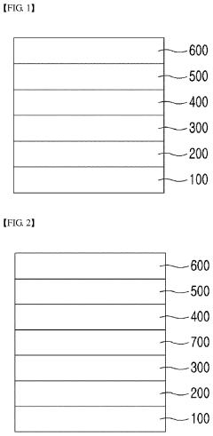
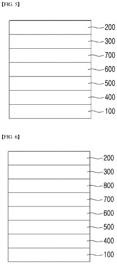
01 Structure and composition of PMA MTJ devices
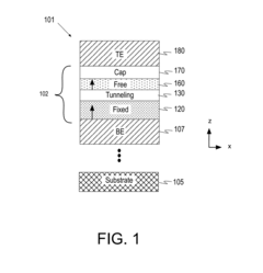
Magnetic Tunnel Junctions with Perpendicular Magnetic Anisotropy (PMA MTJ) can be constructed with specific layer structures and material compositions to enhance performance. These structures typically include a reference layer, a tunnel barrier layer, and a free layer. The materials used often include CoFeB, MgO, and various heavy metals. The thickness and composition of these layers are critical for achieving strong perpendicular magnetic anisotropy, which improves thermal stability and reduces the critical current needed for switching.- Structure and composition of PMA-MTJ devices: Magnetic Tunnel Junctions with Perpendicular Magnetic Anisotropy (PMA-MTJ) can be constructed with specific layer structures and material compositions to enhance performance. These structures typically include a reference layer, tunnel barrier, and free layer with carefully selected materials to maintain strong perpendicular anisotropy. Common materials include CoFeB for magnetic layers and MgO for the tunnel barrier, with specific thickness ratios and interfacial engineering to optimize the perpendicular magnetic properties and tunneling magnetoresistance ratio.
- Enhancement techniques for PMA in MTJ devices: Various techniques can be employed to enhance the perpendicular magnetic anisotropy in MTJ devices. These include interface engineering between the magnetic layers and oxide layers, insertion of ultrathin heavy metal layers, thermal annealing under specific conditions, and doping of magnetic layers with elements like Ta, W, or Hf. These enhancement techniques aim to increase the energy barrier between magnetic states, improve thermal stability, and maintain strong PMA while ensuring high tunneling magnetoresistance.
- Integration of PMA-MTJs in MRAM applications: PMA-MTJs are integrated into Magnetoresistive Random Access Memory (MRAM) devices through specific fabrication processes and circuit designs. The integration involves connecting MTJs with selection transistors, implementing word lines and bit lines for addressing, and incorporating sense amplifiers for read operations. Advanced MRAM designs may use spin-transfer torque (STT) or spin-orbit torque (SOT) writing mechanisms to switch the magnetization of the free layer while maintaining the perpendicular magnetic anisotropy for long-term data retention.
- Switching mechanisms in PMA-MTJ devices: Different switching mechanisms are employed in PMA-MTJ devices to change the magnetization state of the free layer. These include spin-transfer torque (STT), spin-orbit torque (SOT), voltage-controlled magnetic anisotropy (VCMA), and field-assisted switching. Each mechanism offers different advantages in terms of switching speed, energy efficiency, and reliability. The design of the MTJ stack and surrounding circuitry is optimized based on the chosen switching mechanism while maintaining strong perpendicular magnetic anisotropy for stable operation.
- Reliability and thermal stability of PMA-MTJs: Ensuring reliability and thermal stability is crucial for PMA-MTJ devices, particularly in memory applications. Various approaches are implemented to enhance these aspects, including engineering the thickness and composition of magnetic layers, optimizing the interface between layers, incorporating synthetic antiferromagnetic structures, and developing specialized capping layers. These techniques aim to increase the thermal stability factor (Δ), reduce read and write errors, extend device lifetime, and maintain consistent performance across varying operating conditions.
02 Interface engineering for enhanced PMA
Interface engineering plays a crucial role in enhancing perpendicular magnetic anisotropy in MTJs. By carefully controlling the interface between the ferromagnetic layers and adjacent materials, the surface anisotropy can be significantly increased. Techniques include insertion of ultrathin layers, interface oxidation control, and atomic-level manipulation of the interface structure. These approaches can lead to stronger PMA, improved thermal stability, and more efficient spin-transfer torque switching in MTJ devices.Expand Specific Solutions03 Fabrication methods for PMA MTJs
Advanced fabrication methods are essential for creating high-performance PMA MTJs. These methods include precise deposition techniques such as sputtering with controlled parameters, annealing processes to crystallize the MgO barrier and promote perpendicular orientation, and etching procedures to define device structures. Post-deposition treatments like thermal annealing under magnetic fields can further enhance the perpendicular magnetic anisotropy. The fabrication sequence and conditions significantly impact the quality and performance of the resulting MTJ devices.Expand Specific Solutions04 Integration of PMA MTJs in memory applications
PMA MTJs are increasingly integrated into various memory applications, particularly in STT-MRAM (Spin-Transfer Torque Magnetic Random Access Memory). The perpendicular magnetic anisotropy allows for higher density memory arrays, better scalability, and improved energy efficiency compared to in-plane MTJs. Integration challenges include maintaining PMA properties during back-end-of-line processing, addressing thermal stability concerns, and ensuring compatibility with CMOS technology. Advanced circuit designs and sensing schemes are developed to maximize the performance of PMA MTJ-based memory systems.Expand Specific Solutions05 Novel materials and structures for enhanced PMA MTJ performance
Research on novel materials and structures aims to further improve PMA MTJ performance. These innovations include synthetic antiferromagnetic reference layers, dual MgO barriers for enhanced tunnel magnetoresistance, incorporation of Heusler alloys or topological materials, and development of voltage-controlled magnetic anisotropy structures. Other approaches involve strain engineering, doping of magnetic layers, and exploration of 2D materials as tunnel barriers. These advancements target higher thermal stability, lower switching current, faster switching speed, and greater tunnel magnetoresistance ratio.Expand Specific Solutions
Leading Research Groups and Companies in MTJ Development
The magnetic tunnel junction (MTJ) interfacial engineering market is currently in a growth phase, with increasing demand for advanced memory solutions driving innovation. The global MRAM market, where PMA (Perpendicular Magnetic Anisotropy) enhancement is critical, is projected to reach $5-7 billion by 2028. Major semiconductor players like Samsung, TSMC, and Intel are competing with specialized MRAM-focused companies such as Shanghai Ciyu and Crocus Technology. The technology maturity varies significantly across competitors, with established players like Samsung and QUALCOMM demonstrating advanced capabilities through extensive patent portfolios, while emerging companies like Hikstor and CETHIK are rapidly developing competitive solutions. Research institutions including Huazhong University and CNRS are contributing fundamental breakthroughs that are accelerating commercial applications.
Samsung Electronics Co., Ltd.
Technical Solution: Samsung has developed advanced interfacial engineering techniques for enhancing perpendicular magnetic anisotropy (PMA) in magnetic tunnel junctions (MTJs). Their approach focuses on precise control of the CoFeB/MgO interface through optimized deposition processes and post-annealing treatments. Samsung has pioneered the use of ultrathin insertion layers (such as Ta, Hf, or W) between the CoFeB and capping layers to enhance PMA. Their research demonstrates that controlling the crystallization process of the CoFeB layer during annealing significantly improves the magnetic properties at the CoFeB/MgO interface. Samsung has achieved MTJs with thermal stability factors exceeding 60 and tunnel magnetoresistance ratios above 200% through their interfacial engineering techniques, making their devices suitable for high-density STT-MRAM applications.
Strengths: Industry-leading manufacturing capabilities allow for precise control of thin film interfaces at scale; extensive experience in memory technologies provides integration advantages. Weaknesses: Their approach may require complex multi-layer structures that increase manufacturing complexity and potentially impact yield rates.
International Business Machines Corp.
Technical Solution: IBM has developed a comprehensive interfacial engineering approach for PMA enhancement in MTJs focusing on both the CoFeB/MgO interface and the underlayer engineering. Their technology utilizes heavy metal underlayers (such as Ta, W, or Pt) with specific crystalline orientations to induce strong spin-orbit coupling effects at interfaces. IBM's research has demonstrated that controlling oxygen migration at the CoFeB/MgO interface through precise oxygen content management during deposition and annealing significantly enhances PMA. They have pioneered the use of synthetic antiferromagnetic (SAF) structures with engineered interfaces to improve thermal stability while maintaining low switching currents. IBM's MTJ devices feature ultra-thin CoFeB layers (1-1.5nm) with carefully engineered interfaces that demonstrate PMA values exceeding 1.5 mJ/m² and TMR ratios above 250% at room temperature.
Strengths: Extensive research infrastructure and deep expertise in spintronics; strong patent portfolio in MTJ technology; demonstrated ability to scale technologies to production. Weaknesses: Their solutions often require sophisticated materials and processing techniques that may be challenging to implement in high-volume manufacturing environments.
Critical Patents and Publications on PMA Enhancement
Magnetic tunnel junction (MTJ) structure with perpendicular magnetic anisotropy (PMA) having an oxide-based PMA-inducing layer and magnetic element including the same
PatentActiveUS10559745B2
Innovation
- The MTJ structure incorporates a substrate with a perpendicular magnetic anisotropic inducing layer and a perpendicular antiferromagnetic layer, generating perpendicular coupling between the antiferromagnetic layer and ferromagnetic layers, which simplifies the structure, reduces overall thickness, and enhances heat treatment stability.

Strained perpendicular magnetic tunnel junction devices
PatentActiveUS20180287050A1
Innovation
- The introduction of lateral strain in the free magnetic layer of the MTJ stack, achieved through the application of compressive stress, enhances the coercive field strength and thermal stability by aligning the strain orthogonally to the magnetic field direction, thereby improving the stability of the MTJ devices.

Materials Science Considerations for MTJ Fabrication
The fabrication of high-performance Magnetic Tunnel Junctions (MTJs) with enhanced Perpendicular Magnetic Anisotropy (PMA) requires careful consideration of materials science principles. The selection of appropriate materials for each layer in the MTJ stack is critical, as the interfacial properties between these layers largely determine the overall performance characteristics of the device.
The ferromagnetic electrodes in MTJs typically consist of CoFeB alloys, with precise control of composition being essential for optimizing magnetic properties. The boron content in these alloys plays a crucial role in promoting amorphous structure formation during deposition, which facilitates subsequent crystallization processes. Research indicates that a boron concentration between 20-30 atomic percent yields optimal results for PMA development after annealing.
Tunnel barrier materials significantly impact both the magnetoresistance ratio and the interfacial anisotropy. MgO has emerged as the preferred barrier material due to its ability to filter specific electron symmetries, resulting in high tunneling magnetoresistance. The crystallographic orientation of MgO is particularly important, with (001) texture providing the strongest PMA effect when interfaced with CoFeB. The barrier thickness must be precisely controlled, typically between 1-2 nm, to balance tunneling current and exchange coupling effects.
Heavy metal underlayers such as Ta, W, Pt, or Pd serve multiple functions in MTJ stacks. These materials provide a template for subsequent layer growth, act as boron sinks during annealing processes, and contribute to spin-orbit coupling effects that enhance PMA. Recent studies have demonstrated that multilayer combinations of these heavy metals can produce synergistic effects, further strengthening interfacial anisotropy.
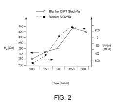
Deposition techniques significantly influence the quality of interfaces in MTJ stacks. Magnetron sputtering remains the industry standard due to its scalability and uniformity, but emerging techniques such as atomic layer deposition offer improved precision for ultrathin layers. Post-deposition annealing processes must be carefully optimized, with temperatures typically between 300-400°C being sufficient to promote crystallization while preventing interdiffusion that could degrade interfaces.
Surface and interface roughness presents a major challenge in MTJ fabrication. Even sub-nanometer scale roughness can disrupt the coherent tunneling process and reduce PMA. Advanced smoothing techniques, including ion beam polishing and surfactant-mediated growth, have been developed to address this issue. Additionally, the incorporation of diffusion barriers and seed layers helps maintain sharp interfaces during both fabrication and subsequent thermal processing.
The ferromagnetic electrodes in MTJs typically consist of CoFeB alloys, with precise control of composition being essential for optimizing magnetic properties. The boron content in these alloys plays a crucial role in promoting amorphous structure formation during deposition, which facilitates subsequent crystallization processes. Research indicates that a boron concentration between 20-30 atomic percent yields optimal results for PMA development after annealing.
Tunnel barrier materials significantly impact both the magnetoresistance ratio and the interfacial anisotropy. MgO has emerged as the preferred barrier material due to its ability to filter specific electron symmetries, resulting in high tunneling magnetoresistance. The crystallographic orientation of MgO is particularly important, with (001) texture providing the strongest PMA effect when interfaced with CoFeB. The barrier thickness must be precisely controlled, typically between 1-2 nm, to balance tunneling current and exchange coupling effects.
Heavy metal underlayers such as Ta, W, Pt, or Pd serve multiple functions in MTJ stacks. These materials provide a template for subsequent layer growth, act as boron sinks during annealing processes, and contribute to spin-orbit coupling effects that enhance PMA. Recent studies have demonstrated that multilayer combinations of these heavy metals can produce synergistic effects, further strengthening interfacial anisotropy.
Deposition techniques significantly influence the quality of interfaces in MTJ stacks. Magnetron sputtering remains the industry standard due to its scalability and uniformity, but emerging techniques such as atomic layer deposition offer improved precision for ultrathin layers. Post-deposition annealing processes must be carefully optimized, with temperatures typically between 300-400°C being sufficient to promote crystallization while preventing interdiffusion that could degrade interfaces.
Surface and interface roughness presents a major challenge in MTJ fabrication. Even sub-nanometer scale roughness can disrupt the coherent tunneling process and reduce PMA. Advanced smoothing techniques, including ion beam polishing and surfactant-mediated growth, have been developed to address this issue. Additionally, the incorporation of diffusion barriers and seed layers helps maintain sharp interfaces during both fabrication and subsequent thermal processing.
Scalability and Integration Challenges for MTJ Technology
The scalability and integration of Magnetic Tunnel Junction (MTJ) technology presents significant challenges as the industry pushes toward higher density memory and logic applications. As device dimensions shrink below 20nm, maintaining sufficient Perpendicular Magnetic Anisotropy (PMA) becomes increasingly difficult due to thermal stability constraints. The interfacial engineering techniques that enhance PMA must be compatible with standard semiconductor manufacturing processes, which introduces additional complexity.
Current integration schemes face critical challenges with etching processes that can damage the delicate magnetic interfaces crucial for PMA. Ion beam etching, commonly used for MTJ patterning, often creates redeposition issues and sidewall damage that degrades device performance. This becomes more pronounced at smaller dimensions where edge effects dominate device behavior, directly impacting the effectiveness of interfacial engineering approaches.
Material compatibility presents another significant hurdle. The thermal budget constraints of CMOS back-end-of-line (BEOL) processing limit annealing temperatures to approximately 400°C, restricting the range of materials and processes available for interface optimization. Many promising PMA-enhancing treatments require higher temperature processing that exceeds these thermal budgets, creating a fundamental integration challenge.
Uniformity and reproducibility across large wafers represent additional scaling concerns. Interfacial engineering techniques must deliver consistent PMA enhancement across 300mm wafers with minimal variation to ensure viable manufacturing yields. Current deposition methods often struggle to maintain the precise atomic-level control required for uniform interfacial properties at this scale, particularly for critical interfaces like CoFeB/MgO where oxygen migration and intermixing must be precisely controlled.
The industry also faces challenges with measurement and characterization at reduced dimensions. As MTJ devices scale below 20nm, conventional magnetic characterization techniques become insufficient for accurately assessing interfacial quality and PMA properties. This creates difficulties in process development and quality control for mass production scenarios.
Parasitic effects become increasingly problematic at smaller nodes. Interfacial diffusion, even at atomic scales, can significantly impact PMA properties when device dimensions are reduced. The proximity of adjacent MTJ cells in high-density arrays can lead to magnetic coupling effects that weren't significant at larger geometries, requiring additional engineering considerations for isolation and shielding.
Addressing these challenges requires holistic approaches that consider not only the fundamental physics of interfacial PMA but also practical manufacturing constraints. Potential solutions include development of low-temperature interface treatments, advanced atomic layer deposition techniques for precise interface control, and novel patterning approaches that minimize damage to critical magnetic interfaces.
Unlock deeper insights with Patsnap Eureka Quick Research — get a full tech report to explore trends and direct your research. Try now!
Generate Your Research Report Instantly with AI Agent
Supercharge your innovation with Patsnap Eureka AI Agent Platform!