Spin-Orbit Torque Switching Strategies For PMA Devices
AUG 22, 20259 MIN READ
Generate Your Research Report Instantly with AI Agent
Patsnap Eureka helps you evaluate technical feasibility & market potential.
SOT-PMA Technology Background and Objectives
Spin-Orbit Torque (SOT) switching has emerged as a promising alternative to conventional Spin-Transfer Torque (STT) technology for magnetic memory and logic applications. The evolution of SOT technology can be traced back to the early 2010s when researchers began exploring novel mechanisms for manipulating magnetization without directly passing current through the magnetic tunnel junction (MTJ). This approach offers significant advantages in terms of energy efficiency, switching speed, and device endurance.
The technological evolution of SOT has been closely linked with advancements in materials science, particularly in the development of heavy metal layers with strong spin-orbit coupling properties such as Pt, Ta, and W. These materials, when interfaced with ferromagnetic layers exhibiting perpendicular magnetic anisotropy (PMA), create systems where current-induced spin accumulation can efficiently switch the magnetization direction.
PMA devices represent a critical component in modern spintronic applications due to their superior thermal stability, scalability, and compatibility with CMOS technology. The combination of SOT switching mechanisms with PMA materials creates a powerful technological platform that addresses many limitations of conventional magnetic memory technologies.
The primary objective of SOT-PMA technology development is to achieve reliable, fast, and energy-efficient switching of magnetic states in nanoscale devices. Current research aims to optimize the switching efficiency by exploring various material combinations, device geometries, and control mechanisms. Particular emphasis is placed on reducing the critical current density required for switching while maintaining robust thermal stability.
Another key goal is to overcome the fundamental challenge of deterministic switching in PMA devices using SOT. Unlike in-plane magnetized systems, PMA devices typically require an additional symmetry-breaking mechanism, such as an external magnetic field or engineered structural asymmetry, to achieve deterministic switching. Finding field-free solutions that are compatible with high-density integration represents a significant technological hurdle.
The technology trajectory indicates a clear trend toward more sophisticated multilayer structures that combine various functional layers to enhance SOT efficiency. Recent breakthroughs in antiferromagnetic and topological materials have opened new avenues for SOT device engineering, potentially enabling even faster switching speeds and lower power consumption.
As the technology matures, research objectives are increasingly focused on practical implementation challenges, including process integration, reliability testing, and scaling behavior. The ultimate goal is to develop SOT-PMA devices that can serve as building blocks for next-generation non-volatile memory, neuromorphic computing systems, and high-frequency spintronic oscillators.
Market Analysis for SOT-MRAM Applications
The SOT-MRAM market is experiencing significant growth potential as emerging memory technologies continue to address the limitations of conventional memory solutions. Current market projections indicate that the global MRAM market, including SOT-MRAM, is expected to reach approximately $5 billion by 2028, with a compound annual growth rate exceeding 25% from 2023 to 2028. SOT-MRAM specifically is positioned to capture a substantial portion of this growth due to its superior performance characteristics compared to conventional STT-MRAM.
The primary market drivers for SOT-MRAM adoption include increasing demand for high-speed, non-volatile memory solutions in data centers, automotive electronics, industrial automation, and Internet of Things (IoT) applications. The technology's ability to combine the speed of SRAM with the non-volatility of flash memory creates a compelling value proposition for system designers seeking to optimize power consumption while maintaining performance.
Data center applications represent the largest potential market segment for SOT-MRAM, with an estimated market share of 35-40%. The technology's low latency, high endurance, and non-volatility make it particularly suitable for cache memory and storage class memory applications in server environments where performance and reliability are paramount.
The automotive sector presents another substantial growth opportunity, projected to grow at over 30% annually through 2028. Advanced driver-assistance systems (ADAS), autonomous driving technologies, and in-vehicle infotainment systems all require robust, high-performance memory solutions capable of operating in harsh environmental conditions—characteristics that align well with SOT-MRAM's capabilities.
Consumer electronics applications, including smartphones, tablets, and wearable devices, are expected to adopt SOT-MRAM technology as manufacturers seek to extend battery life while maintaining or improving device performance. This segment is projected to account for approximately 20% of the total SOT-MRAM market by 2026.
Industrial applications, including factory automation, robotics, and smart grid technologies, represent another significant market opportunity. The industrial segment values SOT-MRAM's radiation hardness, temperature stability, and unlimited write endurance—qualities that are essential in mission-critical systems operating in challenging environments.
Market penetration challenges include competition from established memory technologies such as DRAM and NAND flash, as well as emerging alternatives like RRAM and PCM. Additionally, manufacturing scalability and cost considerations remain significant barriers to widespread adoption, though economies of scale are expected to gradually reduce production costs as volume increases.
Regional analysis indicates that North America and Asia-Pacific will dominate the SOT-MRAM market, with respective market shares of approximately 40% and 35%, driven by the concentration of semiconductor manufacturers and technology companies in these regions.
Current Challenges in SOT Switching for PMA Devices
Despite significant advancements in Spin-Orbit Torque (SOT) switching for Perpendicular Magnetic Anisotropy (PMA) devices, several critical challenges continue to impede the full realization of this technology's potential. One of the primary obstacles remains the high current density requirement for reliable switching, typically in the order of 10^7-10^8 A/cm², which leads to substantial power consumption and thermal management issues in practical applications. This challenge is particularly pronounced in scaled-down devices where heat dissipation becomes increasingly problematic.
The deterministic switching of PMA devices without external magnetic fields represents another significant hurdle. While field-free switching has been demonstrated through various approaches such as exchange bias, geometrical asymmetry, and ferroelectric coupling, each method introduces additional complexities in fabrication processes and material integration, often compromising the scalability and uniformity of device performance.
Material interface engineering presents persistent challenges, as the quality of interfaces between heavy metal layers and ferromagnetic materials critically determines SOT efficiency. Atomic-level defects, intermixing, and oxidation at these interfaces can significantly degrade spin current generation and transmission, resulting in inconsistent switching behavior across devices. The development of robust fabrication techniques that ensure atomically clean and well-defined interfaces remains an ongoing challenge.
Scaling issues further complicate SOT implementation in high-density memory applications. As device dimensions shrink below 20nm, quantum confinement effects and surface phenomena begin to dominate, altering the magnetic properties and spin transport characteristics in unpredictable ways. Additionally, the stochastic nature of the switching process becomes more pronounced at smaller scales, affecting reliability and error rates.
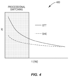
The speed-energy trade-off continues to challenge researchers, with sub-nanosecond switching requiring disproportionately higher energy input. Current experimental demonstrations achieving switching speeds below 200 picoseconds typically demand current densities that exceed practical limits for commercial applications, highlighting the need for more energy-efficient switching mechanisms.
Thermal stability also remains a critical concern, particularly for applications requiring data retention over extended periods. The inherent conflict between easy switchability and long-term stability necessitates careful material engineering and device design optimization. Furthermore, the temperature dependence of SOT switching parameters introduces reliability concerns across operating temperature ranges typical in consumer and industrial electronics.
Finally, integration challenges with CMOS technology present significant barriers to commercialization. The compatibility of SOT materials and processes with standard semiconductor fabrication flows, particularly regarding thermal budget constraints and contamination risks, requires extensive development work before large-scale manufacturing becomes viable.
The deterministic switching of PMA devices without external magnetic fields represents another significant hurdle. While field-free switching has been demonstrated through various approaches such as exchange bias, geometrical asymmetry, and ferroelectric coupling, each method introduces additional complexities in fabrication processes and material integration, often compromising the scalability and uniformity of device performance.
Material interface engineering presents persistent challenges, as the quality of interfaces between heavy metal layers and ferromagnetic materials critically determines SOT efficiency. Atomic-level defects, intermixing, and oxidation at these interfaces can significantly degrade spin current generation and transmission, resulting in inconsistent switching behavior across devices. The development of robust fabrication techniques that ensure atomically clean and well-defined interfaces remains an ongoing challenge.
Scaling issues further complicate SOT implementation in high-density memory applications. As device dimensions shrink below 20nm, quantum confinement effects and surface phenomena begin to dominate, altering the magnetic properties and spin transport characteristics in unpredictable ways. Additionally, the stochastic nature of the switching process becomes more pronounced at smaller scales, affecting reliability and error rates.
The speed-energy trade-off continues to challenge researchers, with sub-nanosecond switching requiring disproportionately higher energy input. Current experimental demonstrations achieving switching speeds below 200 picoseconds typically demand current densities that exceed practical limits for commercial applications, highlighting the need for more energy-efficient switching mechanisms.
Thermal stability also remains a critical concern, particularly for applications requiring data retention over extended periods. The inherent conflict between easy switchability and long-term stability necessitates careful material engineering and device design optimization. Furthermore, the temperature dependence of SOT switching parameters introduces reliability concerns across operating temperature ranges typical in consumer and industrial electronics.
Finally, integration challenges with CMOS technology present significant barriers to commercialization. The compatibility of SOT materials and processes with standard semiconductor fabrication flows, particularly regarding thermal budget constraints and contamination risks, requires extensive development work before large-scale manufacturing becomes viable.
Current SOT Switching Mechanisms and Strategies
01 Current-driven SOT switching mechanisms
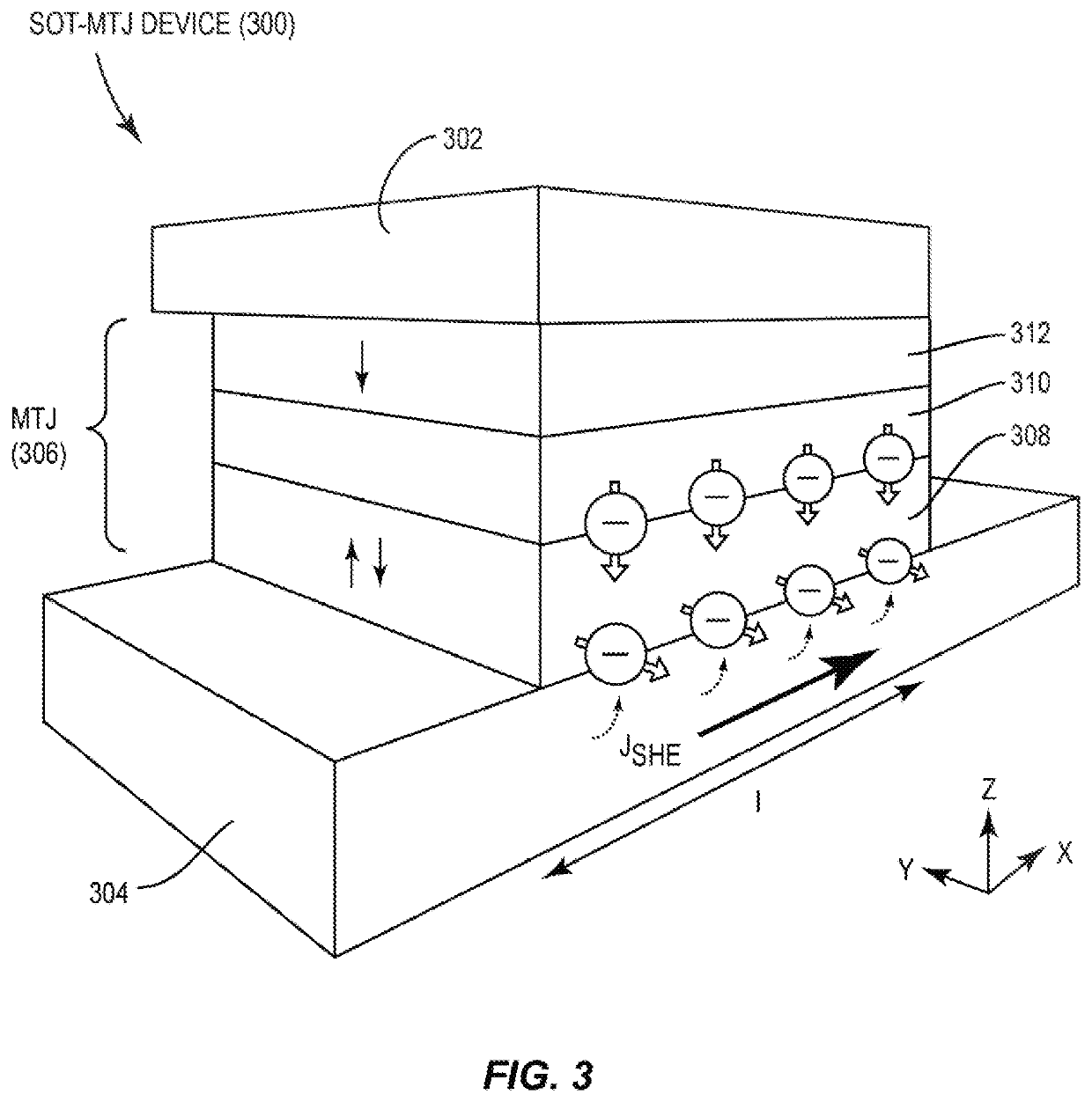
Spin-Orbit Torque (SOT) switching can be achieved through current-driven mechanisms where an in-plane current generates a spin accumulation at the interface between a heavy metal and a ferromagnetic layer. This spin accumulation exerts a torque on the magnetization of the ferromagnetic layer, causing it to switch. The efficiency of this switching mechanism depends on the material properties, interface quality, and current density. Various heavy metals such as Pt, Ta, and W are commonly used to enhance the SOT effect due to their strong spin-orbit coupling.- Field-free SOT switching mechanisms: Field-free spin-orbit torque switching can be achieved through various mechanisms that eliminate the need for external magnetic fields. These approaches include using structures with built-in asymmetry, engineered interfaces, or materials with specific magnetic anisotropy properties. By creating a gradient in magnetic properties or utilizing interfacial effects, these mechanisms enable deterministic switching of magnetic elements without requiring external field assistance, which is crucial for practical memory and logic applications.
- SOT switching with perpendicular magnetic anisotropy: Spin-orbit torque switching strategies for materials with perpendicular magnetic anisotropy (PMA) involve specialized approaches to overcome energy barriers. These strategies include optimizing the heavy metal/ferromagnet interface, engineering the thickness and composition of magnetic layers, and utilizing multi-layer structures. PMA materials are particularly valuable for high-density memory applications as they provide thermal stability while maintaining efficient switching characteristics when properly designed.
- Current-induced SOT switching optimization: Optimization of current-induced spin-orbit torque switching focuses on reducing the critical current density required for reliable magnetic state reversal. This involves engineering the spin Hall angle of heavy metal layers, optimizing the thickness ratio between different materials, and designing current path geometries. Advanced techniques include pulse shaping, where the amplitude and duration of current pulses are precisely controlled to achieve more energy-efficient switching while maintaining high reliability and fast operation.
- SOT device structures and integration: Novel device structures for spin-orbit torque applications include three-terminal configurations, multi-layer stacks with specialized interfaces, and integration with CMOS technology. These structures are designed to enhance switching efficiency, reduce power consumption, and improve scalability. Integration approaches focus on compatibility with semiconductor manufacturing processes, addressing thermal budget constraints, and ensuring reliable electrical connections between the SOT elements and control circuitry for memory and logic applications.
- SOT switching for memory applications: Spin-orbit torque switching strategies specifically tailored for memory applications focus on achieving high endurance, fast operation, and reliable data retention. These include specialized writing schemes that minimize read disturbance, multi-bit storage approaches using domain wall manipulation, and hybrid designs that combine SOT with other switching mechanisms. Advanced memory architectures leverage SOT's advantages of speed and endurance while addressing challenges related to scaling, thermal stability, and integration with sensing circuitry.
02 Field-assisted SOT switching techniques
Field-assisted SOT switching involves the application of an external magnetic field to break the symmetry and facilitate deterministic switching of the magnetization. This approach combines the advantages of SOT with the directional control provided by the external field. The field can be applied in various configurations, such as in-plane or out-of-plane, depending on the device structure and desired switching characteristics. Field-assisted techniques can significantly reduce the critical current required for switching and improve the reliability of the switching process.Expand Specific Solutions03 SOT switching in magnetic memory devices
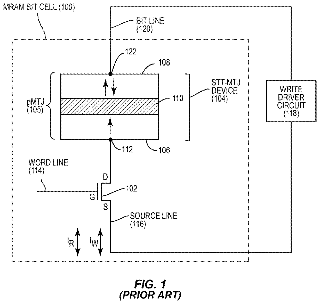
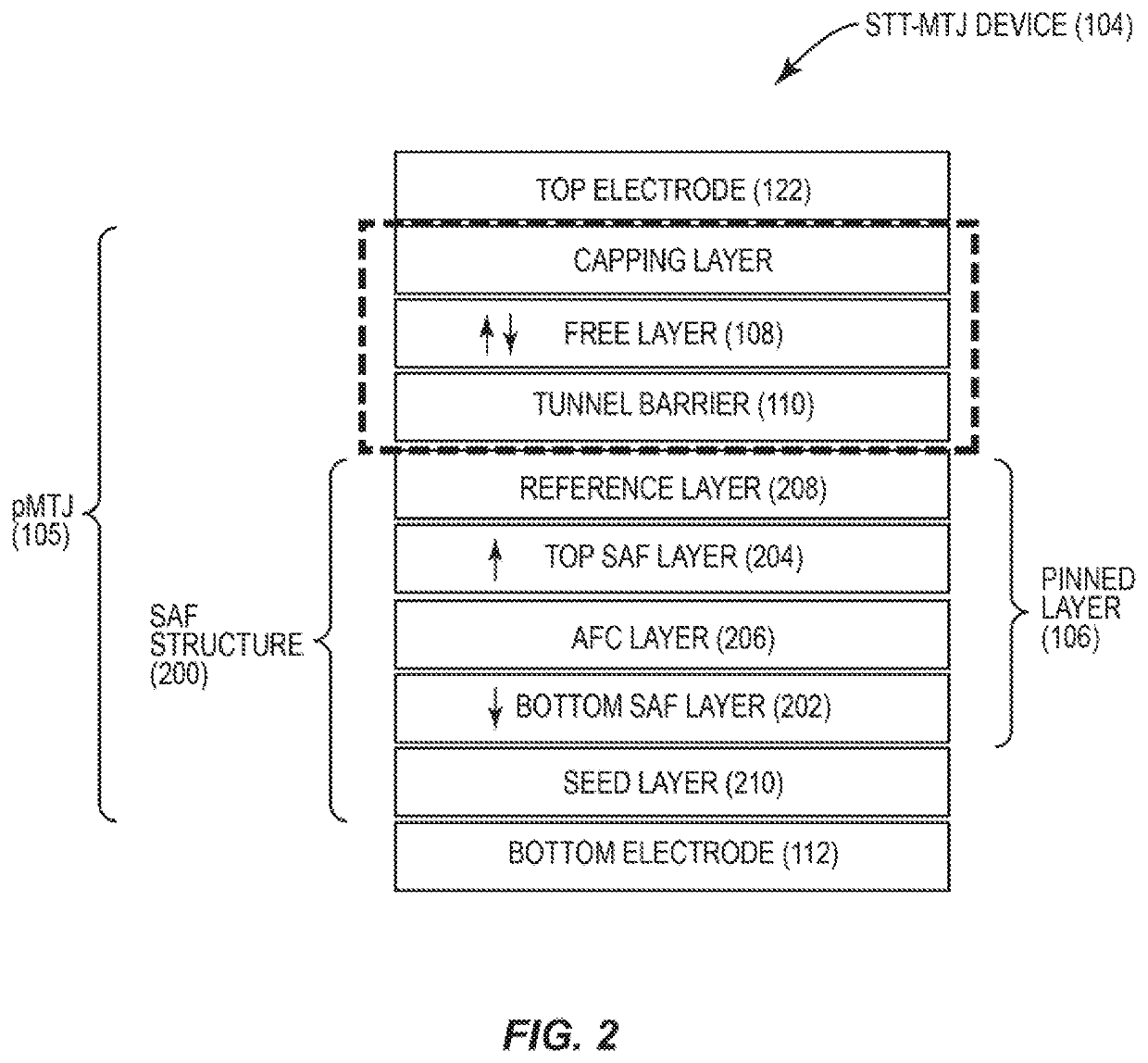
SOT switching is increasingly being implemented in magnetic memory devices such as MRAM (Magnetic Random Access Memory) due to its advantages in terms of energy efficiency and scalability. In these devices, the SOT mechanism is used to switch the free layer of a magnetic tunnel junction (MTJ), which serves as the storage element. The integration of SOT switching in memory devices requires careful design of the write and read paths, as well as consideration of thermal stability and reliability. Advanced device architectures may incorporate multiple layers and novel materials to optimize the SOT effect.Expand Specific Solutions04 Material engineering for enhanced SOT efficiency
Material engineering plays a crucial role in enhancing SOT switching efficiency. This includes the development of novel material stacks, interface engineering, and doping strategies. Heavy metals with strong spin-orbit coupling, topological insulators, and antiferromagnetic materials are being explored to increase the spin Hall angle and reduce the critical current density required for switching. Additionally, the thickness and composition of the ferromagnetic layer can be optimized to improve the efficiency of angular momentum transfer and reduce energy consumption during switching.Expand Specific Solutions05 Three-terminal SOT device architectures
Three-terminal SOT device architectures separate the write and read paths, offering advantages in terms of reliability and endurance compared to conventional two-terminal MTJ devices. In these structures, the SOT switching is induced by current flowing through a heavy metal channel, while the readout is performed through the MTJ stack. This separation allows for independent optimization of the write and read operations, reducing the stress on the tunnel barrier and extending device lifetime. Various geometries and material combinations are being explored to maximize the performance of three-terminal SOT devices.Expand Specific Solutions
Key Industry Players in SOT-MRAM Development
Spin-Orbit Torque (SOT) switching for PMA devices is currently in the early growth phase of industry development, with the market expected to reach significant scale as magnetic memory technologies evolve. The technology is approaching commercial maturity, with key players advancing different implementation strategies. Intel, Samsung, and TSMC are leading industrial development with substantial patent portfolios, while academic institutions like National University of Singapore and Tohoku University contribute fundamental research breakthroughs. Research institutes including the Chinese Academy of Sciences and Max Planck Society are bridging theoretical understanding with practical applications. The competitive landscape shows a balance between established semiconductor giants investing in manufacturing infrastructure and specialized companies like TDK and Headway Technologies focusing on materials optimization and device integration.
Taiwan Semiconductor Manufacturing Co., Ltd.
Technical Solution: TSMC has developed an innovative SOT switching platform for PMA devices that leverages their advanced semiconductor manufacturing processes. Their approach focuses on material engineering and process integration to create highly efficient SOT-MRAM cells compatible with their logic technology nodes. TSMC's solution utilizes a specialized heavy metal/ferromagnet interface with enhanced spin-orbit coupling, achieving spin Hall angles approaching 0.4 in their optimized stack structures[4]. Their SOT devices demonstrate reliable switching with current densities below 5×10^6 A/cm² and switching times under 400 picoseconds. A key innovation in TSMC's approach is their patented field-free switching mechanism that employs engineered structural asymmetry within the device, eliminating the need for external magnetic fields during operation. This makes their technology particularly suitable for embedded memory applications. TSMC has successfully demonstrated integration of these SOT-MRAM cells with their 22nm and 16nm logic processes, showing excellent retention characteristics (thermal stability factor >60) and endurance exceeding 10^12 cycles[5].
Strengths: Seamless integration with advanced CMOS logic processes, excellent scalability potential down to sub-10nm nodes, and demonstrated reliability metrics suitable for commercial applications. Weaknesses: Higher process complexity adding to manufacturing costs, challenges in maintaining uniform switching characteristics across large arrays, and relatively higher write current requirements compared to conventional embedded memories.
Intel Corp.
Technical Solution: Intel has developed a comprehensive SOT switching technology for PMA devices targeting high-performance computing applications. Their approach focuses on materials engineering to maximize the spin Hall effect while ensuring compatibility with their advanced logic processes. Intel's SOT-MRAM technology utilizes a specialized heavy metal layer (primarily beta-phase tungsten with topological insulator interfaces) that achieves spin Hall angles exceeding 0.5, significantly higher than conventional materials[6]. Their three-terminal device architecture separates the read and write paths, enabling sub-nanosecond switching speeds while maintaining high read stability. Intel has demonstrated reliable field-free switching through engineered interface asymmetry and built-in exchange coupling, eliminating the need for external magnetic fields during operation. Their devices show switching current densities as low as 4×10^6 A/cm² with pulse widths of 200-300 picoseconds[7]. Intel has successfully integrated these SOT devices with their 14nm and 10nm process nodes, demonstrating excellent endurance (>10^15 cycles) and retention characteristics suitable for last-level cache applications.
Strengths: Industry-leading integration with advanced logic processes, extremely high endurance compared to other non-volatile memories, and demonstrated compatibility with high-performance computing requirements. Weaknesses: Higher write energy compared to SRAM, larger cell size due to three-terminal structure, and challenges in achieving uniform switching behavior across large arrays at advanced technology nodes.
Critical Patents and Research in SOT-PMA Integration
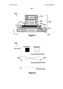
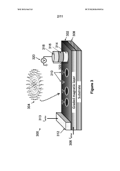
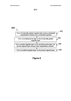
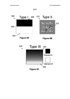
Spin-orbit torque device and material for a spin-orbit torque device
PatentWO2021066743A1
Innovation
- A spin-orbit torque device utilizing a functionally graded magnetic layer with a composition gradient to create bulk-like spin torque, allowing for a thick magnetic layer without compromising efficiency, and enabling a single-layer structure that simplifies fabrication and provides thermal stability.
Spin-orbit torque (SOT) magnetic tunnel junction (MTJ) (sot-MTJ) devices employing perpendicular and in-plane free layer magnetic anisotropy to facilitate perpendicular magnetic orientation switching, suitable for use in memory systems for storing data
PatentInactiveUS20200066968A1
Innovation
- Incorporating both perpendicular magnetic anisotropy (PMA) and in-plane magnetic anisotropy (IMA) regions in the free layer of SOT-MTJ devices, where PMA regions facilitate switching and IMA regions generate an effective magnetic field to maintain deterministic switching after the SOT switching current is removed.
Materials Science Advancements for SOT-PMA Devices
The advancement of materials science has been pivotal in the development of Spin-Orbit Torque (SOT) switching for Perpendicular Magnetic Anisotropy (PMA) devices. Recent breakthroughs in material engineering have significantly enhanced the efficiency and reliability of SOT-PMA devices, marking a transformative era in spintronics technology.
Heavy metals such as Pt, Ta, and W have traditionally served as the foundation for SOT generation due to their strong spin-orbit coupling properties. However, the latest research has revealed that topological insulators (TIs) like Bi2Se3 and BiSb exhibit substantially higher spin-orbit torque efficiency, with reported values exceeding those of conventional heavy metals by an order of magnitude. This dramatic improvement stems from the unique surface states of TIs, which facilitate robust spin-momentum locking.
Engineered interfaces between ferromagnetic layers and SOT-generating materials have emerged as another critical area of materials advancement. Researchers have demonstrated that inserting ultrathin layers of materials like Hf or Mg at these interfaces can significantly modify the magnetic damping and enhance SOT efficiency. Additionally, the development of synthetic antiferromagnets (SAFs) has provided a pathway to reduce stray fields while maintaining thermal stability in SOT-PMA devices.
Novel ferromagnetic materials with optimized PMA characteristics represent another frontier in materials science for these devices. CoFeB-based alloys with precise control of boron content and crystallization behavior have shown excellent PMA properties when interfaced with MgO. Furthermore, rare-earth transition metal alloys like GdFeCo offer unique advantages through their compensation points, where angular momentum transfer becomes highly efficient.
The integration of 2D materials such as graphene and transition metal dichalcogenides (TMDs) has opened new possibilities for SOT devices. These atomically thin materials provide exceptional interface quality and unique spin-transport properties that can be leveraged for next-generation SOT switching schemes.
Multilayer heterostructures combining various material systems have demonstrated remarkable synergistic effects. For instance, TI/ferromagnet/heavy metal trilayers have shown enhanced SOT efficiency through complementary spin current generation mechanisms. These complex material stacks enable engineering of both interfacial and bulk properties to optimize device performance.
Advanced deposition techniques, including molecular beam epitaxy and atomic layer deposition, have been instrumental in achieving precise control over material properties at the atomic scale. These techniques enable the growth of high-quality crystalline structures with minimal defects, which is essential for maximizing SOT efficiency and device reliability in practical applications.
Energy Efficiency Comparison with Competing Memory Technologies
When comparing the energy efficiency of Spin-Orbit Torque (SOT) switching in Perpendicular Magnetic Anisotropy (PMA) devices with competing memory technologies, several critical factors must be considered. SOT-based magnetic memory demonstrates significant advantages in terms of power consumption, particularly during write operations, where it can achieve switching energies in the sub-fJ range per bit under optimal conditions.
Compared to conventional SRAM technology, SOT-MRAM offers substantially lower static power consumption due to its non-volatile nature, eliminating the need for constant power to maintain stored information. While SRAM provides faster access times (typically 1-10ns), its energy consumption per bit operation (10-100fJ) and substantial leakage current make it less efficient for applications where power constraints are paramount.
DRAM, though more dense than SRAM, requires periodic refresh operations that consume additional energy. SOT-MRAM eliminates this refresh requirement, resulting in energy savings particularly in standby scenarios. The energy per bit operation for DRAM typically ranges from 2-10pJ, significantly higher than the projected efficiency of optimized SOT devices.
Flash memory, while non-volatile like SOT-MRAM, suffers from high write energies (100pJ-10nJ per bit) and limited endurance (10^4-10^5 cycles). In contrast, SOT-MRAM can achieve endurance exceeding 10^12 cycles with write energies potentially below 100fJ per bit when implementing advanced switching strategies such as voltage-controlled magnetic anisotropy assistance.
Conventional STT-MRAM, the closest competitor to SOT-MRAM, typically requires 100fJ-1pJ per switching operation. SOT switching strategies demonstrate a theoretical advantage by decoupling the read and write paths, reducing the critical current density required for switching by approximately an order of magnitude compared to STT approaches.
Recent experimental demonstrations have shown that SOT devices with optimized materials and structures can achieve switching energies approaching 100fJ at sub-ns timescales. This represents a significant improvement over STT-MRAM, particularly when considering the reduced write latency and superior endurance characteristics of SOT devices.
The energy efficiency advantage becomes even more pronounced when considering system-level metrics. The reduced write current requirements of SOT devices translate to smaller transistor sizes in the peripheral circuitry, further decreasing the overall energy footprint of memory arrays. Additionally, the faster switching speeds enable more energy-efficient computing paradigms where memory operations constitute a smaller fraction of the total computational energy budget.
Unlock deeper insights with Patsnap Eureka Quick Research — get a full tech report to explore trends and direct your research. Try now!
Generate Your Research Report Instantly with AI Agent
Supercharge your innovation with Patsnap Eureka AI Agent Platform!