Materials With Perpendicular Magnetic Anisotropy: Fundamentals And Device Relevance
AUG 22, 20259 MIN READ
Generate Your Research Report Instantly with AI Agent
Patsnap Eureka helps you evaluate technical feasibility & market potential.
PMA Materials Evolution and Research Objectives
Materials with perpendicular magnetic anisotropy (PMA) have evolved significantly over the past several decades, transforming from scientific curiosities to critical components in modern spintronic devices. The journey began in the 1960s with the discovery of PMA in rare earth-transition metal alloys, but gained substantial momentum in the 1990s when ultrathin Co/Pt and Co/Pd multilayers demonstrated robust PMA properties suitable for technological applications.
The evolution of PMA materials has been driven by the increasing demands of data storage technologies. Early magnetic recording media utilized in-plane magnetic anisotropy, but as storage density requirements increased, the superparamagnetic limit became a significant barrier. PMA materials emerged as a solution by enabling smaller bit sizes while maintaining thermal stability, thus allowing continued scaling of magnetic storage devices.
A pivotal advancement occurred in the mid-2000s with the discovery of interfacial PMA in CoFeB/MgO structures, which revolutionized magnetic random access memory (MRAM) development. This breakthrough combined the advantages of high tunnel magnetoresistance with the stability offered by perpendicular magnetic orientation, setting the stage for commercially viable spin-transfer torque MRAM devices.
Recent years have witnessed the exploration of novel material systems including synthetic antiferromagnets, Heusler alloys, and topological materials that exhibit PMA. These materials promise enhanced performance characteristics such as lower switching currents, higher thermal stability, and reduced stray fields, addressing key challenges in spintronic device implementation.
The current research objectives in PMA materials focus on several critical areas. First, enhancing the magnetic anisotropy energy density to improve thermal stability without compromising other magnetic properties. Second, reducing the damping constant to enable more energy-efficient switching in memory and logic applications. Third, developing materials with tunable PMA that can be controlled via external stimuli such as electric fields, offering pathways to ultra-low power electronics.
Additionally, researchers aim to understand and exploit interfacial phenomena that give rise to PMA, particularly at metal/oxide interfaces where spin-orbit coupling plays a crucial role. The integration of PMA materials with emerging technologies such as neuromorphic computing and quantum information processing represents another frontier, where the unique properties of these materials could enable novel functionalities.
The ultimate goal is to develop PMA materials that simultaneously satisfy multiple requirements: high thermal stability, low switching energy, CMOS compatibility, and reliability over billions of operation cycles. Achieving these objectives would not only advance existing applications like MRAM but could potentially enable entirely new paradigms in computing and information processing technologies.
Market Demand Analysis for PMA-based Devices
The global market for devices based on materials with Perpendicular Magnetic Anisotropy (PMA) has experienced significant growth over the past decade, primarily driven by the increasing demand for high-density data storage solutions. The data storage industry represents the largest market segment for PMA-based technologies, with an estimated market value exceeding $80 billion in 2023 and projected to reach $110 billion by 2027, growing at a CAGR of approximately 8.2%.
Magnetic Random Access Memory (MRAM) utilizing PMA materials has emerged as a particularly promising technology, addressing the growing need for non-volatile memory solutions that combine the speed of SRAM, the density of DRAM, and the non-volatility of flash memory. The MRAM market segment is expected to grow from $1.2 billion in 2023 to $5.3 billion by 2028, representing one of the fastest-growing segments within the semiconductor memory industry.
The automotive and industrial sectors have also shown increasing interest in PMA-based devices, particularly for applications requiring reliable operation in harsh environments. These sectors value the radiation hardness, temperature stability, and long-term data retention capabilities of PMA-based memory solutions. Market analysis indicates that automotive applications for PMA-based devices will grow at a CAGR of 12.5% through 2027.
Consumer electronics represents another significant market driver, with smartphone manufacturers increasingly adopting PMA-based components for improved performance and energy efficiency. The integration of PMA materials in sensors and memory components for mobile devices has created a market segment valued at approximately $3.7 billion in 2023.
Geographically, North America and Asia-Pacific dominate the market for PMA-based devices, collectively accounting for over 75% of global demand. China, Japan, South Korea, and the United States lead in both production and consumption of these technologies, with European markets showing accelerated adoption rates in recent years.
Industry surveys indicate that key customer requirements for PMA-based devices include improved energy efficiency (cited by 87% of potential enterprise customers), increased data retention capabilities (82%), reduced form factor (76%), and enhanced operational stability across varying environmental conditions (71%). These market demands directly align with the inherent advantages of PMA materials.
The competitive landscape is characterized by significant R&D investments from both established semiconductor manufacturers and specialized startups. Venture capital funding for startups focused on PMA-based technologies has exceeded $2.1 billion since 2020, indicating strong investor confidence in the market potential of these technologies.
Current PMA Technology Landscape and Challenges
The global landscape of Perpendicular Magnetic Anisotropy (PMA) technology has evolved significantly over the past decade, with major advancements in materials science and device engineering. Currently, the field is dominated by multilayer thin film structures, particularly Co/Pt and Co/Pd interfaces, which have demonstrated robust PMA properties suitable for commercial applications. These materials have become foundational in spintronics devices, particularly in Magnetic Random Access Memory (MRAM) technologies.
Despite significant progress, several critical challenges persist in PMA technology development. Material stability remains a primary concern, as many PMA materials exhibit degradation under thermal stress and repeated magnetic switching cycles. This degradation manifests as reduced anisotropy strength and compromised magnetic properties over time, limiting device longevity and reliability in practical applications.
Interface quality control presents another substantial challenge. The PMA effect is highly sensitive to atomic-level interface characteristics, making manufacturing consistency difficult to achieve at industrial scales. Even minor variations in interface roughness, interdiffusion, or crystalline defects can significantly alter PMA properties, resulting in device-to-device performance variations that complicate large-scale production.
Energy efficiency in PMA-based devices continues to be a limiting factor. Current materials require relatively high current densities for magnetic switching, leading to power consumption concerns in mobile and IoT applications. This challenge is particularly acute in spin-transfer torque MRAM (STT-MRAM) technologies, where reducing critical switching current while maintaining thermal stability remains an ongoing research focus.
Scalability represents perhaps the most pressing challenge for next-generation applications. As device dimensions approach sub-10nm scales, maintaining sufficient PMA strength becomes increasingly difficult due to thermal fluctuations and edge effects. Researchers are actively exploring novel material combinations and engineered interfaces to address this scaling limitation.
The geographical distribution of PMA technology development shows concentration in East Asia (particularly Japan and South Korea), North America, and Western Europe. Major semiconductor manufacturers and research institutions in these regions have established significant intellectual property portfolios in PMA materials and devices, creating a competitive landscape dominated by established players with advanced fabrication capabilities.
Recent innovations in PMA technology include the exploration of rare-earth transition metal alloys, synthetic antiferromagnets, and topological materials with unique spin-orbit coupling properties. These emerging approaches aim to overcome the fundamental limitations of conventional PMA materials while enabling new functionalities for next-generation spintronic devices.
Current PMA Implementation Approaches
01 Multilayer structures for enhanced perpendicular magnetic anisotropy
Multilayer structures consisting of alternating layers of magnetic and non-magnetic materials can enhance perpendicular magnetic anisotropy (PMA). These structures typically include ferromagnetic layers sandwiched between heavy metal layers or oxide interfaces that promote strong interfacial anisotropy. The thickness and composition of each layer can be precisely controlled to optimize the PMA properties, making these structures suitable for high-density magnetic storage applications and spintronic devices.- Multilayer structures for PMA materials: Multilayer structures consisting of alternating layers of magnetic and non-magnetic materials can exhibit strong perpendicular magnetic anisotropy. These structures typically include ferromagnetic layers (such as Co, Fe, or their alloys) sandwiched between non-magnetic layers (such as Pt, Pd, or oxide materials). The interfaces between these layers create the conditions necessary for perpendicular magnetic anisotropy, making them suitable for high-density magnetic storage applications and spintronic devices.
- PMA in magnetic tunnel junctions and MRAM: Perpendicular magnetic anisotropy materials are crucial components in magnetic tunnel junctions (MTJs) and magnetoresistive random-access memory (MRAM) devices. These materials enable the creation of stable, perpendicular magnetization that can be switched with lower current densities compared to in-plane magnetization. The perpendicular configuration allows for higher storage densities and improved thermal stability, making these devices more efficient and reliable for data storage applications.
- Rare earth and transition metal alloys for PMA: Alloys combining rare earth elements with transition metals can exhibit strong perpendicular magnetic anisotropy. Materials such as TbFeCo, GdFeCo, and similar compositions have been developed to achieve high magnetic anisotropy energy density. These alloys are particularly valuable in applications requiring thermally stable magnetic properties and are often used in magneto-optical recording media and specialized magnetic devices where high coercivity and temperature stability are required.
- Interface-induced PMA in thin films: Perpendicular magnetic anisotropy can be induced at the interfaces between thin magnetic films and adjacent layers. This interface effect is particularly strong in systems where magnetic metals interface with oxides (such as CoFeB/MgO) or heavy metals (such as Co/Pt). The interfacial PMA arises from spin-orbit coupling and hybridization of electronic orbitals at the interface. By controlling the thickness and composition of these interfaces, the strength of the perpendicular anisotropy can be tuned for specific applications.
- PMA materials for heat-assisted magnetic recording: Materials with perpendicular magnetic anisotropy are essential for heat-assisted magnetic recording (HAMR) technology. These materials typically have high anisotropy energy that provides thermal stability at room temperature but can be temporarily reduced at elevated temperatures during the writing process. FePt-based alloys in the L10 ordered phase are particularly important for this application due to their exceptionally high magnetic anisotropy. The development of these materials has enabled significant increases in data storage density in hard disk drives.
02 Rare earth and transition metal alloys for PMA materials
Alloys combining rare earth elements with transition metals exhibit strong perpendicular magnetic anisotropy due to their unique crystalline structure and electronic configurations. These materials, such as TbFeCo, GdFeCo, and SmCo, demonstrate high magnetic coercivity and thermal stability, making them excellent candidates for magnetic recording media and permanent magnet applications. The ratio of rare earth to transition metal can be adjusted to fine-tune the magnetic properties for specific applications.Expand Specific Solutions03 PMA materials for magnetic random access memory (MRAM)
Materials with perpendicular magnetic anisotropy are crucial for developing high-performance magnetic random access memory devices. These materials enable the creation of magnetic tunnel junctions with enhanced thermal stability, reduced switching current, and improved data retention. Common PMA materials for MRAM include CoFeB/MgO interfaces, Co/Pt multilayers, and various ferromagnetic/heavy metal heterostructures that facilitate efficient spin-orbit torque switching while maintaining high tunnel magnetoresistance ratios.Expand Specific Solutions04 Novel fabrication methods for PMA materials
Advanced fabrication techniques have been developed to create materials with enhanced perpendicular magnetic anisotropy. These methods include magnetron sputtering with precise control of deposition parameters, molecular beam epitaxy for atomically precise interfaces, and post-deposition annealing processes to optimize crystalline structure. Additional techniques involve ion irradiation to modify interfacial properties and the use of seed layers to control crystallographic orientation, all contributing to improved PMA characteristics.Expand Specific Solutions05 PMA materials for heat-assisted magnetic recording
Heat-assisted magnetic recording (HAMR) technology utilizes materials with perpendicular magnetic anisotropy that can maintain high coercivity at room temperature while becoming writable when locally heated. These materials often incorporate elements such as FePt in the L10 ordered phase, which exhibits extremely high magnetic anisotropy. The development of these materials focuses on optimizing grain size, thermal stability, and switching field distribution to achieve higher recording densities while ensuring reliable data storage performance.Expand Specific Solutions
Key Industry Players in PMA Materials Research
Materials with Perpendicular Magnetic Anisotropy (PMA) technology is currently in a growth phase, with the global market expanding as data storage demands increase. The technology has reached moderate maturity, with key players advancing its commercial viability. Leading companies like Samsung Electronics, SK Hynix, Western Digital, and Seagate Technology are driving innovation in PMA materials for high-density storage applications. Research institutions including CEA, CNRS, and various universities collaborate with industry leaders to overcome technical challenges. The competitive landscape features established semiconductor manufacturers and specialized materials companies working to enhance PMA performance for next-generation memory devices, with Asian companies particularly dominant in commercialization efforts.
Commissariat à l´énergie atomique et aux énergies Alternatives
Technical Solution: CEA has developed advanced perpendicular magnetic anisotropy (PMA) materials for spintronic applications, focusing on CoFeB/MgO interfaces that exhibit strong PMA properties. Their technical approach involves precise control of interface quality through optimized deposition techniques and post-annealing processes. CEA has pioneered the development of magnetic tunnel junctions (MTJs) with PMA that demonstrate thermal stability at sub-20nm dimensions while maintaining high tunnel magnetoresistance ratios exceeding 200%. Their research has established critical thickness thresholds for CoFeB layers (1.0-1.4nm) where maximum PMA is achieved, and they've developed innovative buffer and capping layer structures to enhance PMA properties. CEA has also explored voltage-controlled magnetic anisotropy (VCMA) in these materials, demonstrating electric field modulation of magnetic properties for low-power switching applications in MRAM devices.
Strengths: Exceptional expertise in interface engineering for PMA optimization; strong integration capabilities with CMOS technology; comprehensive understanding of PMA physics enabling device optimization. Weaknesses: Scaling challenges below 10nm where thermal stability and PMA strength may degrade; potential reliability issues with repeated voltage-induced switching in VCMA applications.
Seagate Technology LLC
Technical Solution: Seagate has developed specialized PMA materials optimized for heat-assisted magnetic recording (HAMR) and microwave-assisted magnetic recording (MAMR) technologies. Their technical approach centers on FePt-based L10 ordered alloys with extremely high magnetic anisotropy (>70 Merg/cm³) enabling thermal stability at ultra-high recording densities beyond 2 Tb/in². Seagate's proprietary granular media design incorporates carefully engineered segregants (primarily SiO2 and TiO2) to control grain size distribution and intergranular exchange coupling. Their manufacturing process includes precise control of substrate heating during deposition to promote L10 ordering while maintaining narrow grain size distribution (σ/D < 0.2). Seagate has pioneered dual-layer PMA media structures with gradient anisotropy profiles that optimize writability while maintaining thermal stability. Recent innovations include incorporation of rare earth dopants to fine-tune Curie temperature and anisotropy field temperature dependence, enabling more efficient energy-assisted recording processes with reduced writing fields.
Strengths: Industry-leading expertise in high-anisotropy recording media; demonstrated capability to manufacture PMA materials at scale for commercial hard drives; sophisticated understanding of thermal effects on PMA properties. Weaknesses: Extremely high anisotropy materials require energy-assisted recording techniques, increasing system complexity; challenges with controlling grain size distribution at ultra-high densities.
Critical Patents and Breakthroughs in PMA Technology
Magnetic device
PatentActiveJP2020155445A
Innovation
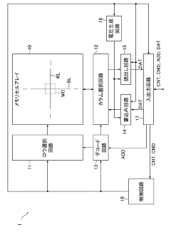
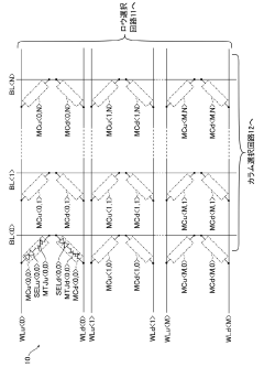
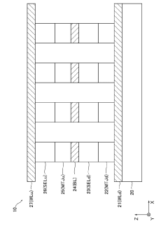
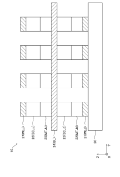
- A magnetic device with a specific configuration of nonmagnetic and ferromagnetic materials, including a nonmagnetic rare earth oxide, is used to enhance perpendicular magnetic anisotropy while suppressing parasitic resistance by controlling the thickness and composition of nonmagnetic layers to facilitate boron absorption and crystal growth.
Magnetic device
PatentInactiveJP2020043224A
Innovation
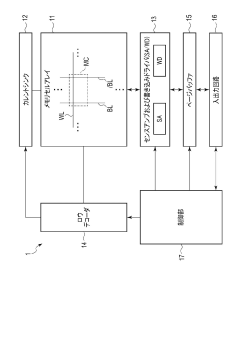
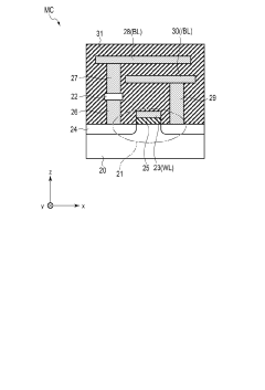
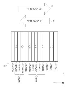
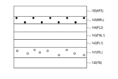
- A magnetic device comprising a magnetoresistive element with ferromagnetic layers antiferromagnetically coupled via ferromagnetic nitride layers, which includes a specific laminated structure of ferromagnetic and non-magnetic layers to enhance perpendicular magnetic anisotropy and magnetoresistive properties.
Manufacturing Processes for PMA Materials
The manufacturing of materials with Perpendicular Magnetic Anisotropy (PMA) requires sophisticated processes that balance precision, scalability, and cost-effectiveness. Current industrial manufacturing approaches primarily utilize physical vapor deposition (PVD) techniques, with sputtering being the most widely adopted method due to its excellent control over film thickness and composition.
Magnetron sputtering represents the industry standard for PMA material fabrication, allowing for precise deposition of multilayer structures with controlled interfaces. This process typically operates in ultra-high vacuum conditions (10^-8 to 10^-9 Torr) to minimize contamination and ensure high-quality interfaces between layers. For complex PMA structures like CoFeB/MgO interfaces, the deposition parameters must be tightly controlled, with substrate temperatures typically maintained between 20-300°C depending on the specific material system.
Post-deposition annealing represents a critical manufacturing step that significantly influences PMA properties. Thermal annealing at temperatures ranging from 250-400°C promotes crystallization at interfaces (particularly in CoFeB/MgO systems) and enhances the perpendicular anisotropy. The annealing duration and temperature profile must be precisely controlled to avoid interdiffusion that could degrade magnetic properties.
Alternative manufacturing techniques include molecular beam epitaxy (MBE), which offers superior control over layer growth but at significantly higher costs and lower throughput compared to sputtering. MBE is primarily utilized in research settings or for specialized applications requiring atomically precise interfaces.
Emerging manufacturing approaches include atomic layer deposition (ALD) for ultrathin barrier layers and pulsed laser deposition (PLD) for specialized material systems. These techniques offer advantages in terms of conformality and stoichiometric control but have not yet achieved widespread industrial adoption for PMA materials.
Lithographic patterning of PMA materials presents additional manufacturing challenges, particularly as device dimensions shrink below 20nm. Electron beam lithography offers the necessary resolution but suffers from low throughput, while optical lithography techniques struggle with the required precision for advanced spintronic devices.
Quality control in PMA manufacturing relies heavily on advanced characterization techniques including X-ray reflectivity for thickness measurements, vibrating sample magnetometry for magnetic property verification, and transmission electron microscopy for interface analysis. In-line monitoring systems are increasingly being integrated into production lines to enable real-time process adjustments and maintain consistent material properties across production batches.
Energy Efficiency Impact of PMA-based Devices
The implementation of Perpendicular Magnetic Anisotropy (PMA) materials in spintronic devices represents a significant breakthrough in addressing energy efficiency challenges in modern computing systems. PMA-based devices fundamentally alter the energy landscape of magnetic storage and processing technologies by enabling significant reductions in critical switching currents compared to their in-plane magnetization counterparts.
The energy consumption advantage stems primarily from PMA's inherent physical properties. In conventional in-plane magnetic devices, switching magnetization requires overcoming substantial demagnetization fields, resulting in higher energy requirements. PMA materials, by contrast, align magnetization perpendicular to the film plane, dramatically reducing the energy barrier for magnetization reversal. Quantitative analyses demonstrate that PMA-based Magnetic Tunnel Junctions (MTJs) can achieve switching with current densities approximately one order of magnitude lower than traditional designs.
This efficiency translates directly to practical applications. In Spin-Transfer Torque Magnetic Random Access Memory (STT-MRAM), PMA-based cells demonstrate 60-80% lower write energy compared to in-plane alternatives while maintaining thermal stability. The reduced current requirements also mitigate issues related to dielectric breakdown in tunnel barriers, enhancing device reliability and longevity. These improvements address critical bottlenecks in memory hierarchies where energy consumption during write operations has traditionally limited widespread adoption.
Beyond memory applications, PMA materials enable novel computing paradigms with inherent energy advantages. In neuromorphic computing implementations, PMA-based synaptic devices demonstrate power consumption in the sub-pJ range per synaptic operation, positioning them as viable alternatives to CMOS-based neural networks that typically require orders of magnitude more energy. Similarly, in logic applications, PMA-based magnetic logic gates show promising energy-delay products that could eventually challenge conventional semiconductor approaches.
The system-level impact of PMA technology extends to data centers and mobile devices. Projections indicate that widespread implementation of PMA-based memory could reduce overall data center energy consumption by 8-12%, primarily through the elimination of refresh operations required in conventional DRAM and reduction in leakage power. For battery-powered devices, the non-volatile nature of PMA-based memory combined with its energy efficiency could extend operational time between charges by 15-20% in typical usage scenarios.
As manufacturing processes mature, these energy efficiency benefits are expected to improve further through materials optimization and device architecture refinements, potentially establishing PMA-based technologies as the foundation for next-generation energy-efficient computing systems.
Unlock deeper insights with Patsnap Eureka Quick Research — get a full tech report to explore trends and direct your research. Try now!
Generate Your Research Report Instantly with AI Agent
Supercharge your innovation with Patsnap Eureka AI Agent Platform!
