Roadmap For PMA Material Adoption In Commercial MRAM
AUG 22, 20259 MIN READ
Generate Your Research Report Instantly with AI Agent
Patsnap Eureka helps you evaluate technical feasibility & market potential.
PMA Material Evolution and MRAM Development Goals
Perpendicular Magnetic Anisotropy (PMA) materials have emerged as a critical technology enabler for Magnetoresistive Random Access Memory (MRAM), evolving significantly over the past two decades. The initial PMA materials utilized in research settings were primarily based on Co/Pt or Co/Pd multilayers, which demonstrated strong perpendicular anisotropy but presented challenges for integration into semiconductor manufacturing processes due to their complex multilayer structures and material incompatibilities.
The evolution trajectory shifted toward CoFeB-based PMA systems around 2010, when researchers at AIST and Tohoku University demonstrated that CoFeB/MgO interfaces could generate sufficient PMA for practical MRAM applications. This breakthrough represented a pivotal moment, as it aligned with existing semiconductor manufacturing capabilities and offered a path toward commercial viability.
Subsequent development focused on enhancing the thermal stability factor (Δ) while maintaining low switching current density. The industry established clear benchmarks: achieving Δ > 60 for 10-year data retention and reducing critical switching current density below 5 MA/cm² for energy efficiency. These parameters have guided material optimization efforts across the field.
Material composition refinements have been systematic, with varying Fe:Co ratios in CoFeB demonstrating different PMA strengths. The introduction of insertion layers and seed layers has further enhanced performance, with Ta, W, Mo, and Hf emerging as effective materials for promoting strong PMA characteristics while improving thermal endurance.
Recent advancements have focused on synthetic antiferromagnetic (SAF) structures and novel material systems like Heusler alloys and rare-earth transition metal alloys. These materials promise higher spin polarization and stronger anisotropy, potentially enabling sub-10nm MRAM devices with improved performance metrics.
The development goals for commercial MRAM have evolved from initial demonstrations to specific performance targets. Current objectives include achieving write endurance exceeding 10^12 cycles, reducing bit-to-bit variability below 5%, and ensuring thermal stability at operating temperatures up to 125°C for automotive and industrial applications.
Looking forward, the roadmap for PMA materials in MRAM targets scaling capabilities to 5nm technology nodes and below, with particular emphasis on materials that can maintain performance at reduced dimensions. The industry is also pursuing materials compatible with back-end-of-line (BEOL) processing temperatures exceeding 400°C to enable broader integration options in semiconductor manufacturing flows.
Market Analysis for Commercial MRAM Applications
The global MRAM market is experiencing significant growth, projected to reach $1.6 billion by 2026 with a CAGR of approximately 39% from 2021. This remarkable expansion is driven by increasing demand for non-volatile memory solutions that combine the speed of SRAM, the density of DRAM, and the non-volatility of flash memory. PMA (Perpendicular Magnetic Anisotropy) materials represent a critical advancement in MRAM technology, enabling higher density, improved thermal stability, and lower power consumption compared to traditional in-plane magnetic approaches.
Commercial applications for PMA-based MRAM span multiple sectors. In automotive electronics, MRAM is gaining traction for advanced driver assistance systems (ADAS) and infotainment systems, where its radiation hardness and temperature stability provide significant advantages. The industrial automation sector values MRAM's reliability in harsh environments and instant-on capabilities for critical control systems. Consumer electronics manufacturers are increasingly adopting MRAM for smartphones, wearables, and IoT devices due to its low power consumption and fast write speeds.
Enterprise storage systems represent another substantial market opportunity, with MRAM serving as cache memory or buffer storage in SSDs and enterprise storage arrays. The aerospace and defense sectors are adopting MRAM for mission-critical systems where data integrity under extreme conditions is paramount. Additionally, the emerging edge computing paradigm creates demand for memory solutions that can operate efficiently with limited power resources, making MRAM an attractive option.
Regional analysis reveals that North America currently leads MRAM adoption, particularly in enterprise storage and aerospace applications. Asia-Pacific represents the fastest-growing market, driven by consumer electronics manufacturing and automotive applications in countries like Japan, South Korea, and China. Europe shows strong adoption in industrial automation and automotive sectors, particularly in Germany and France.
Market barriers include relatively high production costs compared to established memory technologies, manufacturing complexity for advanced PMA materials, and competition from alternative emerging memory technologies such as ReRAM and PCRAM. However, as production scales and manufacturing processes mature, the cost differential is expected to narrow significantly by 2025.
Key market drivers include the growing need for energy-efficient computing solutions, expansion of edge computing infrastructure, increasing complexity of automotive electronics, and the persistent demand for faster, more reliable non-volatile memory in data centers. The transition from in-plane to PMA-based MRAM represents a pivotal shift that will likely accelerate commercial adoption across these diverse application domains.
Current PMA Material Challenges in MRAM Technology
Perpendicular Magnetic Anisotropy (PMA) materials represent a critical advancement in MRAM technology, yet their implementation faces significant technical challenges. Current commercial MRAM devices predominantly utilize CoFeB/MgO-based structures, which exhibit limitations in thermal stability and scalability below the 20nm node. The interfacial PMA derived from these structures provides insufficient anisotropy energy for next-generation high-density applications, creating a fundamental barrier to further miniaturization.
Material stability presents another major challenge, as PMA materials must maintain their magnetic properties during the high-temperature processes (up to 400°C) required for CMOS integration. Many promising PMA candidates demonstrate degraded performance after thermal annealing, with interdiffusion at material interfaces compromising the critical magnetic properties. This thermal instability significantly narrows the viable material selection for commercial implementation.
Achieving precise control over magnetic parameters represents a substantial manufacturing hurdle. The PMA strength, damping factor, and saturation magnetization must be carefully balanced to optimize both writing efficiency and data retention. Current deposition techniques struggle to maintain the nanometer-precision layer thicknesses and atomically sharp interfaces required for consistent PMA behavior across large-diameter wafers, resulting in device-to-device variability that impacts manufacturing yield.
The industry also faces challenges in scaling PMA material production from laboratory demonstrations to high-volume manufacturing environments. Many promising research materials utilize rare elements or complex deposition processes that prove difficult to implement in standard semiconductor fabrication facilities. The lack of established supply chains for specialized materials further complicates industrial adoption.
Reliability concerns persist regarding PMA material degradation mechanisms under operational conditions. Write endurance limitations, where repeated switching events gradually degrade magnetic properties, remain inadequately characterized for many advanced PMA systems. Similarly, long-term data retention behavior under various environmental stresses requires more comprehensive understanding to meet the 10+ year retention requirements of commercial memory products.
Etching and patterning processes present additional complications, as conventional semiconductor techniques can damage the magnetic properties of PMA materials through edge oxidation, ion implantation damage, or compositional changes. These processing-induced defects often concentrate at the edges of magnetic elements, precisely where they most significantly impact device performance in scaled MRAM cells.
The industry must also address the limited understanding of spin-orbit torque mechanisms in novel PMA materials, as this knowledge gap hinders the development of optimized writing schemes for next-generation SOT-MRAM devices that promise improved performance and reliability over conventional STT-MRAM approaches.
Current PMA Material Integration Solutions for MRAM
01 PMA material applications in electronic devices
Polymethyl acrylate (PMA) materials are increasingly adopted in electronic device manufacturing due to their excellent electrical properties and thermal stability. These materials are used in components like displays, batteries, and circuit boards. The adoption of PMA materials has enabled the development of more efficient and durable electronic devices with improved performance characteristics.- PMA material applications in electronic devices: Polymethyl acrylate (PMA) materials are increasingly adopted in electronic device manufacturing due to their excellent electrical properties and thermal stability. These materials are used in components like displays, circuit boards, and semiconductor packaging. The adoption of PMA materials has enabled the development of thinner, more flexible electronic devices with improved durability and performance characteristics.
- PMA material integration in communication systems: Communication systems have benefited from the integration of PMA materials in various components. These materials provide enhanced signal transmission properties and reduced interference, making them valuable in network infrastructure equipment and mobile devices. The adoption of PMA materials has contributed to improvements in bandwidth capacity, signal clarity, and overall communication system reliability.
- PMA material implementation in software and data management: PMA materials have been implemented in data storage and management systems, offering improved data retention capabilities and system performance. These materials enable more efficient software execution environments and enhance data processing capabilities. The adoption of PMA-based solutions has led to advancements in cloud computing infrastructure, data centers, and enterprise software systems.
- PMA material utilization in manufacturing processes: Manufacturing industries have adopted PMA materials to enhance production processes and product quality. These materials offer benefits such as improved adhesion, durability, and resistance to environmental factors. The integration of PMA materials in manufacturing has led to more efficient production methods, reduced waste, and enhanced product performance across various industrial applications.
- PMA material innovation in emerging technologies: Emerging technologies have embraced PMA materials for their versatile properties and adaptability. These materials are being incorporated into innovations such as IoT devices, smart systems, and advanced computing platforms. The adoption of PMA materials in these cutting-edge applications has facilitated the development of more responsive, efficient, and sustainable technological solutions.
02 PMA material integration in communication systems
Communication systems benefit from PMA material adoption through enhanced signal transmission and reception capabilities. These materials provide improved insulation properties and resistance to environmental factors, making them ideal for telecommunications infrastructure. The integration of PMA materials in communication systems has led to better network performance, reduced interference, and increased reliability in various operating conditions.Expand Specific Solutions03 PMA material implementation in software and data management
Software systems and data management platforms are incorporating PMA material principles for improved functionality. This implementation allows for better data processing, storage efficiency, and system integration. The adoption of PMA-based approaches in software architecture enables more robust performance monitoring, adaptive resource allocation, and enhanced user experience across various applications.Expand Specific Solutions04 PMA material utilization in manufacturing processes
Manufacturing industries are adopting PMA materials to enhance production processes and product quality. These materials offer advantages such as improved durability, reduced weight, and better resistance to chemicals and environmental factors. The integration of PMA materials in manufacturing has led to cost reductions, increased production efficiency, and the development of innovative products with superior performance characteristics.Expand Specific Solutions05 PMA material innovation for sustainable applications
Recent innovations focus on developing sustainable PMA materials with reduced environmental impact. These advancements include biodegradable variants, recycling methods, and energy-efficient production processes. The adoption of environmentally friendly PMA materials supports sustainability goals while maintaining the performance benefits that make these materials valuable across various industries and applications.Expand Specific Solutions
Leading Companies and Research Institutions in MRAM Development
The MRAM market is currently in a growth phase, with PMA (Perpendicular Magnetic Anisotropy) materials representing a critical advancement path. The global MRAM market is projected to expand significantly, driven by increasing demand for non-volatile memory solutions with DRAM-like performance. Technologically, major players are at varying stages of PMA material adoption. TSMC, Samsung, and SK Hynix lead commercial implementation, while companies like Qualcomm and IBM focus on integration into their systems. Research institutions including IMEC, CNRS, and CEA are advancing fundamental PMA material science. Specialized MRAM developers such as Antaios, Headway Technologies, and Shanghai Ciyu are pushing innovative implementations. The ecosystem shows a collaborative approach between semiconductor manufacturers, research institutions, and specialized memory developers to overcome remaining technical challenges.
Samsung Electronics Co., Ltd.
Technical Solution: Samsung has developed a comprehensive PMA material adoption roadmap for MRAM commercialization focusing on both standalone and embedded applications. Their approach utilizes CoFeB/MgO-based perpendicular MTJs with synthetic antiferromagnetic (SAF) reference layers to enhance thermal stability and reduce stray fields. Samsung's roadmap includes progressive scaling of PMA materials from 28nm to sub-10nm nodes with corresponding improvements in switching efficiency. They've demonstrated functional 8Mb STT-MRAM test chips with PMA-MTJs showing endurance exceeding 10^12 cycles and data retention of over 10 years at 85°C. Samsung's material innovation includes dual-interface PMA enhancement using Ta/CoFeB/MgO/CoFeB/Ta structures and specialized annealing processes (300-400°C) to crystallize the CoFeB while maintaining perpendicular anisotropy. Their roadmap also addresses manufacturing challenges through development of specialized PVD deposition tools with <1% thickness variation across 300mm wafers.
Strengths: Vertical integration capabilities from materials research to mass production; extensive manufacturing infrastructure allowing rapid commercialization; strong position in both standalone and embedded memory markets. Weaknesses: Balancing performance requirements across diverse application segments creates optimization challenges; scaling PMA materials below 10nm faces fundamental physics limitations; competition from alternative emerging memory technologies in their product portfolio.
SK hynix, Inc.
Technical Solution: SK hynix has established a strategic roadmap for PMA material adoption in commercial MRAM focusing on high-density storage applications. Their approach centers on developing perpendicular MTJ stacks with enhanced thermal stability and reduced switching current density. SK hynix's material system utilizes CoFeB/MgO interfaces with specialized seed and cap layers to maximize interfacial perpendicular anisotropy. Their roadmap includes progressive scaling of PMA-MTJs from 28nm to 14nm nodes while maintaining Δ>70 for enterprise storage requirements. SK hynix has demonstrated functional 256Mb STT-MRAM arrays with sub-5ns write speeds and endurance exceeding 10^11 cycles. Their material innovation includes development of composite free layers with engineered damping parameters to optimize switching efficiency. SK hynix's manufacturing approach incorporates multi-step annealing processes to simultaneously optimize crystallization of the CoFeB layers and magnetic properties of the reference layer. Their roadmap also addresses reliability concerns through specialized testing protocols for temperature-dependent performance characterization.
Strengths: Strong expertise in high-volume memory manufacturing; established infrastructure for rapid technology deployment; deep understanding of memory hierarchy requirements for different applications. Weaknesses: Relatively later entry into MRAM market compared to some competitors; challenges in achieving cost parity with established memory technologies; balancing PMA material optimization across diverse product requirements.
Key Patents and Breakthroughs in PMA Material Science
Perpendicular magnetic anisotropy free layers with iron insertion and oxide interfaces for spin transfer torque magnetic random access memory
PatentActiveUS20180226576A1
Innovation
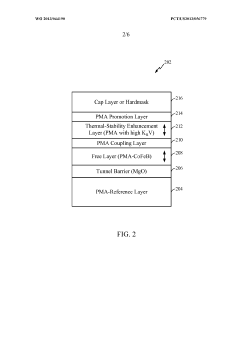
- The method involves forming a tunnel barrier layer and a free layer with a CoFeB alloy and an iron layer, followed by a sputtering process to create a metal oxide layer, which enhances the PMA and reduces the switching current density, achieving at least 50% higher switching efficiency compared to devices with CoFeB alone.
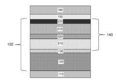
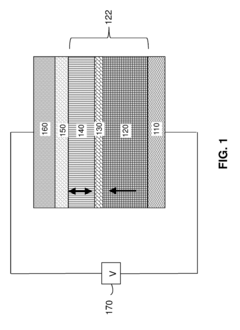
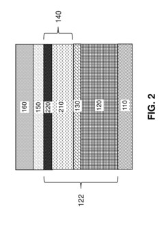
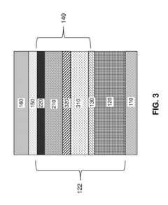
Thermally tolerant perpendicular magnetic anisotropy coupled elements for spin-transfer torque switching device
PatentWO2013044190A1
Innovation
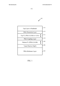
- A magnetic tunnel junction configuration is developed with a composite PMA layer and a PMA coupling layer, using a relatively thick CoFeB layer with an assist layer to enhance perpendicular magnetic anisotropy, thereby increasing thermal stability without increasing switching current density.
Manufacturing Scalability and Cost Analysis
The scalability of PMA (Perpendicular Magnetic Anisotropy) materials for commercial MRAM production presents significant manufacturing challenges that directly impact cost structures. Current fabrication processes for PMA-based MRAM devices require precise control of ultra-thin multilayer stacks, often with layer thicknesses in the angstrom range. This precision requirement necessitates advanced deposition tools such as Physical Vapor Deposition (PVD) systems with enhanced uniformity control, significantly increasing capital equipment costs compared to conventional semiconductor manufacturing lines.
Material consumption efficiency represents another critical cost factor. The rare earth and precious metals commonly used in PMA structures, including platinum, cobalt, and specialized rare earth elements, contribute substantially to raw material expenses. Yield management becomes particularly challenging as PMA material properties are highly sensitive to contamination and process variations. Industry data indicates that yield rates for advanced PMA-MRAM can be 15-20% lower than those for conventional semiconductor devices, directly impacting per-unit costs.
Scaling to higher production volumes requires addressing several manufacturing bottlenecks. The thermal budget constraints of PMA materials limit integration options with standard CMOS processes. Current manufacturing approaches often require dedicated equipment sets and specialized handling protocols to maintain material integrity throughout the fabrication sequence. This separation from standard process flows creates logistical complexities and reduces equipment utilization rates.
Cost modeling analyses suggest that PMA-MRAM manufacturing expenses follow a different scaling curve compared to conventional memory technologies. While traditional semiconductor costs decrease approximately 30% with each node shrink, PMA-MRAM currently achieves only 15-20% cost reduction due to material complexity and process control requirements. This differential presents challenges for competitive positioning against established memory technologies.
The industry is pursuing several approaches to improve manufacturing economics. These include development of multi-chamber deposition systems optimized for PMA stack formation, implementation of in-line metrology for real-time process control, and exploration of alternative material systems that maintain PMA characteristics while using more abundant elements. Equipment suppliers are also developing specialized tools that can process larger wafer batches while maintaining the required precision, potentially reducing per-unit capital costs by 25-30% over the next generation.
Reliability and Endurance Benchmarks for Commercial Adoption
Reliability and endurance metrics represent critical benchmarks for the commercial adoption of PMA (Perpendicular Magnetic Anisotropy) materials in MRAM technology. Current commercial MRAM solutions require a minimum endurance of 10^6 cycles for consumer applications and 10^9-10^12 cycles for enterprise storage and critical systems. PMA-based MRAM must meet or exceed these standards to achieve market acceptance.
Testing data from leading manufacturers indicates that first-generation PMA-MRAM devices demonstrate endurance ratings of approximately 10^7-10^8 cycles, showing promising progress but still falling short for high-performance applications. Temperature stability represents another crucial reliability factor, with commercial requirements demanding stable operation between -40°C and 125°C for automotive and industrial applications.
Data retention capabilities of PMA materials have shown significant improvement, with current research prototypes demonstrating 10-year data retention at 85°C-105°C. This approaches the commercial requirement of 10-year retention at 125°C for automotive-grade memory. However, variability in manufacturing processes continues to impact yield rates and device-to-device consistency.
Write error rates (WER) for PMA-MRAM currently range from 10^-6 to 10^-9, requiring additional error correction mechanisms that increase system complexity. Industry standards for commercial adoption typically demand WER below 10^-11 for enterprise applications, highlighting an area requiring further development.
Radiation hardness testing reveals that PMA-based MRAM exhibits inherent resistance to radiation effects compared to conventional memory technologies, making it particularly suitable for aerospace and military applications where reliability under harsh conditions is paramount. Recent testing by aerospace contractors has demonstrated functionality after exposure to 100 krad total ionizing dose.
Accelerated aging tests suggest that PMA material interfaces may experience degradation after extended thermal cycling, potentially limiting device lifetime. Research indicates that incorporating diffusion barrier layers and optimized capping materials can mitigate this effect, extending the projected operational lifetime to meet the 10-15 year commercial requirement.
To achieve widespread commercial adoption, PMA-MRAM technology must demonstrate reliability metrics comparable to established memory technologies while maintaining its advantages in non-volatility and power consumption. Current roadmaps from major manufacturers project that these benchmarks will be achieved in production devices by 2025-2026, enabling broader market penetration beyond specialized applications.
Unlock deeper insights with Patsnap Eureka Quick Research — get a full tech report to explore trends and direct your research. Try now!
Generate Your Research Report Instantly with AI Agent
Supercharge your innovation with Patsnap Eureka AI Agent Platform!