Chemical Amplification Mechanisms in EUV Resists Materials
OCT 13, 20259 MIN READ
Generate Your Research Report Instantly with AI Agent
Patsnap Eureka helps you evaluate technical feasibility & market potential.
EUV Resist Evolution and Objectives
Extreme Ultraviolet (EUV) lithography represents a revolutionary advancement in semiconductor manufacturing, enabling the continuation of Moore's Law by facilitating the production of increasingly smaller transistors. The evolution of EUV resist materials has been a critical component in this technological progression, with chemical amplification mechanisms playing a pivotal role in enhancing sensitivity and resolution.
The journey of EUV resist development began in the early 2000s, evolving from traditional deep ultraviolet (DUV) resist platforms. Initial EUV resist materials faced significant challenges due to the fundamentally different physics involved in EUV exposure (13.5 nm wavelength) compared to DUV systems. The higher photon energy of EUV radiation (91.6 eV) creates secondary electrons that drive complex chemical reactions within the resist, necessitating novel approaches to chemical amplification.
Chemical amplification in EUV resists operates through a catalytic process where a single photochemical event triggers multiple chemical reactions, amplifying the initial exposure effect. This mechanism has evolved from traditional acid-catalyzed deprotection chemistry to more sophisticated hybrid approaches incorporating metal-organic compounds and nanoparticles to enhance EUV absorption and quantum yield.
The primary objectives in EUV resist development center around the resolution-linewidth roughness-sensitivity (RLS) trade-off. Current industry targets aim for resolutions below 10 nm half-pitch, line edge roughness below 2 nm, and sensitivities better than 20 mJ/cm². These parameters are interdependent, creating a complex optimization challenge that drives continuous innovation in chemical amplification mechanisms.
Recent technological trends show a shift toward non-traditional resist platforms, including metal oxide resists, molecular glasses, and inorganic-organic hybrid systems. These novel materials aim to overcome the fundamental limitations of traditional chemically amplified resists (CARs) by offering improved EUV absorption cross-sections and reduced blur from secondary electron diffusion.
The future trajectory of EUV resist evolution points toward multi-trigger resist systems that combine chemical amplification with other mechanisms such as physical amplification or direct conversion processes. These approaches seek to maintain high sensitivity while improving resolution and reducing pattern collapse at sub-10 nm feature sizes.
Industry collaboration has accelerated in recent years, with consortia like SEMATECH and imec driving standardized evaluation of novel resist platforms. This collaborative approach has been essential in addressing the complex challenges of EUV lithography and establishing clear benchmarks for chemical amplification performance in next-generation semiconductor manufacturing.
Market Analysis for EUV Lithography Materials
The global market for EUV lithography materials, particularly photoresists, has experienced significant growth in recent years, driven by the semiconductor industry's push toward smaller node sizes. The market value for EUV-specific materials reached approximately $500 million in 2022, with projections indicating growth to $1.2 billion by 2027, representing a compound annual growth rate of 19.1%. This growth trajectory is primarily fueled by the increasing adoption of EUV lithography in high-volume manufacturing by leading semiconductor companies.
Chemical amplification mechanisms in EUV resist materials represent a critical segment within this market, accounting for nearly 70% of all EUV resist solutions currently deployed. The demand for chemically amplified resists (CARs) remains strong despite emerging alternatives, as they offer established performance characteristics and integration pathways that newer technologies have yet to match at scale.
Regional analysis reveals that East Asia dominates the market landscape, with South Korea, Taiwan, and Japan collectively representing 68% of global consumption. This concentration aligns with the geographic distribution of advanced semiconductor manufacturing facilities. North America and Europe follow with 18% and 14% market share respectively, primarily driven by research activities and specialized manufacturing operations.
Key market drivers include the continuous miniaturization of semiconductor devices, with leading manufacturers transitioning to 5nm and 3nm process nodes. The chemical amplification mechanisms in EUV resists directly enable this scaling, creating substantial market pull. Additionally, the growing demand for high-performance computing, artificial intelligence applications, and 5G infrastructure has accelerated the need for advanced semiconductor devices, further stimulating market growth.
Customer segmentation shows that integrated device manufacturers (IDMs) and foundries constitute the largest buyer segment at 85% of market volume. Research institutions account for approximately 10%, while specialty applications make up the remaining 5%. This distribution highlights the production-focused nature of the current market.
Pricing trends indicate moderate but consistent increases, with premium EUV resist materials commanding 3-4 times the price of traditional ArF resist materials. This premium pricing reflects both the advanced chemistry required and the critical role these materials play in enabling cutting-edge semiconductor manufacturing processes.
Market challenges include supply chain vulnerabilities, as revealed during recent global disruptions, and increasing environmental regulations affecting chemical manufacturing and handling. Additionally, the high cost of EUV lithography equipment continues to limit broader market adoption, constraining the potential market size for associated materials.
Current Challenges in Chemical Amplification Mechanisms
Despite significant advancements in EUV lithography, chemical amplification mechanisms in EUV resist materials face several critical challenges that impede optimal performance. The fundamental issue lies in the shot noise effect, which becomes increasingly problematic as feature sizes continue to shrink below 10nm. At these dimensions, the statistical variation in photon absorption creates significant line edge roughness (LER) and line width roughness (LWR), compromising pattern fidelity.
The acid diffusion mechanism, central to chemical amplification, presents another major challenge. While necessary for sensitivity enhancement, acid diffusion often extends beyond intended pattern boundaries, causing resolution degradation. This diffusion-resolution trade-off becomes more pronounced in EUV systems where the photon energy (13.5nm wavelength) is significantly higher than in traditional lithography, creating secondary electrons with longer travel distances.
Outgassing during EUV exposure represents a substantial concern for manufacturing environments. The high-energy EUV photons can break chemical bonds in resist materials, releasing volatile compounds that contaminate expensive EUV optics. This contamination reduces mirror reflectivity and ultimately impacts system throughput and lifetime, creating significant economic implications for high-volume manufacturing.
Pattern collapse has emerged as a critical issue as aspect ratios increase in advanced nodes. The capillary forces during development, combined with the reduced mechanical strength of highly sensitive resists, lead to structural failures in fine patterns. This mechanical limitation creates a complex balance between sensitivity requirements and structural integrity.
The stochastic effects in EUV lithography present perhaps the most fundamental challenge. With fewer photons available per unit area compared to traditional lithography, random variations in photon absorption, photoelectron generation, and acid production create significant variability in pattern formation. These stochastic effects establish a theoretical resolution limit that becomes increasingly difficult to overcome.
Material stability under EUV exposure conditions presents ongoing challenges. The high-energy photons can trigger unintended chemical reactions beyond the designed amplification pathways, leading to resist degradation, reduced contrast, and increased defectivity. This necessitates the development of more robust chemical structures specifically engineered for EUV wavelengths.
The sensitivity-resolution-LER triangle continues to constrain EUV resist development, with improvements in one parameter typically coming at the expense of others. Breaking this fundamental trade-off relationship requires novel approaches to chemical amplification mechanisms that can simultaneously address all three parameters.
Existing Chemical Amplification Solutions
01 Chemical amplification mechanisms in EUV resists
Chemical amplification mechanisms are fundamental to EUV resist technology, involving photoacid generators that release acids upon exposure to EUV radiation. These acids catalyze multiple chemical reactions, amplifying the initial photochemical event and increasing sensitivity. The mechanism typically includes deprotection reactions of polymer matrices, changing solubility properties in exposed areas. This amplification process is crucial for achieving high resolution and sensitivity required for EUV lithography.- Chemical amplification mechanisms in EUV resists: Chemical amplification mechanisms are fundamental to EUV resist technology, involving photoacid generators that create acids upon exposure to EUV radiation. These acids catalyze multiple chemical reactions, amplifying the initial photochemical event and increasing sensitivity. The mechanism typically includes acid diffusion through the resist film, followed by deprotection reactions that change the solubility of exposed areas, enabling pattern development. Advanced chemical amplification systems incorporate various catalytic reactions to enhance resolution and sensitivity while minimizing pattern collapse and line edge roughness.
- Metal-containing EUV resist materials: Metal-containing materials have emerged as promising candidates for EUV resists due to their high absorption cross-sections for EUV radiation. These materials incorporate metal atoms or clusters (such as hafnium, zirconium, or tin) into the resist structure, significantly improving sensitivity to EUV wavelengths (13.5 nm). The metal components can be integrated as nanoparticles, organometallic compounds, or metal oxide structures within the resist matrix. These materials offer enhanced pattern fidelity and reduced line edge roughness while requiring lower exposure doses compared to traditional organic resists.
- Hybrid and multi-component resist systems: Hybrid and multi-component resist systems combine different materials and mechanisms to optimize EUV lithography performance. These systems typically integrate organic polymers with inorganic components or blend multiple polymers with varying functionalities. The hybrid approach allows for customization of resist properties including sensitivity, resolution, line edge roughness, and etch resistance. Some systems incorporate nanoparticles or molecular additives that enhance specific properties while maintaining compatibility with existing processing methods. Multi-trigger mechanisms may be employed where pattern formation requires multiple simultaneous or sequential chemical events, improving contrast and reducing pattern blur.
- Non-chemically amplified EUV resist materials: Non-chemically amplified resist materials for EUV lithography operate through direct photochemical reactions rather than catalytic amplification processes. These materials include chain-scission polymers, photo-crosslinking systems, and molecular resists that undergo structural changes directly upon EUV exposure. The absence of diffusion-controlled amplification steps potentially enables higher resolution patterning with improved line edge roughness. These materials often incorporate high EUV absorbing elements or functional groups to compensate for the lack of chemical amplification. Development mechanisms may involve physical property changes such as polarity shifts or solubility alterations triggered directly by radiation.
- Advanced imaging and evaluation techniques for EUV resists: Advanced imaging and evaluation techniques are essential for characterizing and optimizing EUV resist materials and their chemical amplification mechanisms. These include specialized microscopy methods, spectroscopic techniques, and computational modeling approaches that provide insights into resist behavior at the nanoscale. Real-time monitoring of chemical reactions during exposure and development helps understand acid diffusion, deprotection kinetics, and pattern formation dynamics. Techniques such as scanning electron microscopy, atomic force microscopy, and X-ray scattering are employed to evaluate pattern quality, while computational simulations predict resist performance and guide formulation improvements. These methods enable systematic optimization of resist compositions and processing conditions.
02 Metal-containing EUV resist materials
Metal-containing resists represent an important class of EUV materials that incorporate metal atoms or clusters to enhance EUV absorption. These materials typically contain metals such as hafnium, zirconium, or tin that have high EUV absorption cross-sections. The metal components can be integrated into the resist structure as organometallic compounds or metal oxide nanoparticles. These materials offer improved sensitivity due to their higher EUV absorption compared to traditional organic resists.Expand Specific Solutions03 Non-chemically amplified EUV resist systems
Non-chemically amplified resist systems for EUV lithography operate without the traditional acid-catalyzed amplification mechanism. These materials undergo direct structural changes upon EUV exposure, such as chain scission or crosslinking. The approach eliminates issues associated with acid diffusion, potentially improving resolution and line edge roughness. These systems often utilize molecular glass resists, nanoparticle-based materials, or metal oxide resists that change solubility directly upon exposure without requiring a catalytic amplification step.Expand Specific Solutions04 Hybrid and multi-trigger resist mechanisms
Hybrid and multi-trigger resist systems combine multiple reaction pathways to optimize EUV lithography performance. These systems may incorporate both chemical amplification and non-chemically amplified mechanisms, or utilize multiple triggers such as photoacids and photobase generators. The hybrid approach allows for fine-tuning of resist properties including sensitivity, resolution, and line edge roughness. Some systems employ secondary reactions that are activated only after the primary exposure mechanism, providing enhanced control over the patterning process.Expand Specific Solutions05 Additives and sensitizers for EUV resist performance enhancement
Various additives and sensitizers can be incorporated into EUV resist formulations to enhance performance characteristics. These include quenchers to control acid diffusion, sensitizers to improve quantum yield, and plasticizers to modify physical properties. Nanoparticles and molecular additives can be used to enhance sensitivity or improve pattern quality. Specific compounds may be added to reduce line edge roughness or improve adhesion to substrates. The careful selection and optimization of these additives is crucial for achieving the desired balance of sensitivity, resolution, and pattern fidelity in EUV lithography.Expand Specific Solutions
Leading Companies in EUV Resist Development
The EUV resist materials market is in a growth phase, with increasing adoption driven by semiconductor industry demands for higher resolution lithography. The market is expected to expand significantly as EUV technology becomes mainstream in advanced node manufacturing. Leading players include JSR Corp., Tokyo Ohka Kogyo, and Shin-Etsu Chemical, who have established strong positions through extensive R&D in chemical amplification mechanisms. ASML, as the sole EUV lithography equipment provider, collaborates with these materials suppliers, while semiconductor giants like TSMC and Samsung Electronics drive requirements as end-users. Academic institutions including Osaka University and Tsinghua University contribute fundamental research, creating a competitive landscape where established chemical companies compete with specialized newcomers like Irresistible Materials in developing next-generation EUV resist solutions with improved sensitivity, resolution, and line edge roughness.
Shin-Etsu Chemical Co., Ltd.
Technical Solution: Shin-Etsu has developed advanced metal-oxide hybrid EUV resist materials that utilize unique chemical amplification mechanisms. Their technology employs specialized polymer matrices with acid-labile protecting groups that undergo catalytic deprotection upon exposure to EUV radiation. The company's resist formulations incorporate highly sensitive photo-acid generators (PAGs) with optimized absorption cross-sections specifically designed for 13.5nm wavelength. Shin-Etsu's chemical amplification system achieves quantum yields exceeding 10 acid molecules per absorbed photon, significantly enhancing sensitivity while maintaining resolution below 20nm half-pitch patterns. Their proprietary quencher compounds control acid diffusion during post-exposure bake processes, enabling precise pattern formation with minimal line edge roughness (LER values of 2-3nm). The company has also pioneered multi-trigger resist systems where secondary reaction cascades amplify the initial photochemical response, further improving sensitivity-resolution-roughness trade-offs critical for high-volume manufacturing.
Strengths: Industry-leading sensitivity-resolution balance with exceptional chemical amplification efficiency; extensive manufacturing experience ensuring high material consistency. Weaknesses: Higher material costs compared to conventional resists; requires precise process control to manage acid diffusion and prevent pattern collapse at extreme dimensions.
JSR Corp.
Technical Solution: JSR has pioneered metal-containing EUV resist materials with enhanced chemical amplification mechanisms. Their technology utilizes organometallic compounds (particularly containing Sn, Zr, or Hf) that significantly increase EUV absorption cross-sections compared to traditional carbon-based materials. JSR's chemical amplification system employs a dual-action mechanism where the initial photon absorption generates both primary acids and secondary radical species, creating a controlled chain reaction that amplifies the exposure effect. This approach achieves sensitivity values below 20 mJ/cm² while maintaining resolution capabilities for 13nm half-pitch features. The company has developed proprietary quencher molecules that establish concentration gradients within the resist film, allowing precise control over the chemical amplification process and reducing blur effects. JSR's formulations also incorporate specialized polymer matrices with optimized polarity switching mechanisms that enhance development contrast after exposure, resulting in improved pattern fidelity and reduced line edge roughness (typically 2-3nm). Recent innovations include chemically amplified metal-oxide resist systems that combine high etch resistance with enhanced sensitivity.
Strengths: Superior EUV absorption efficiency through metal incorporation; excellent sensitivity-resolution-roughness balance; robust manufacturing capabilities. Weaknesses: More complex formulation requiring stringent quality control; potential for metal contamination concerns in semiconductor processing environments.
Key Innovations in Acid Generation Chemistry
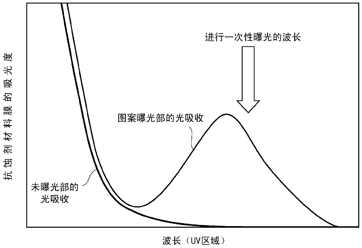
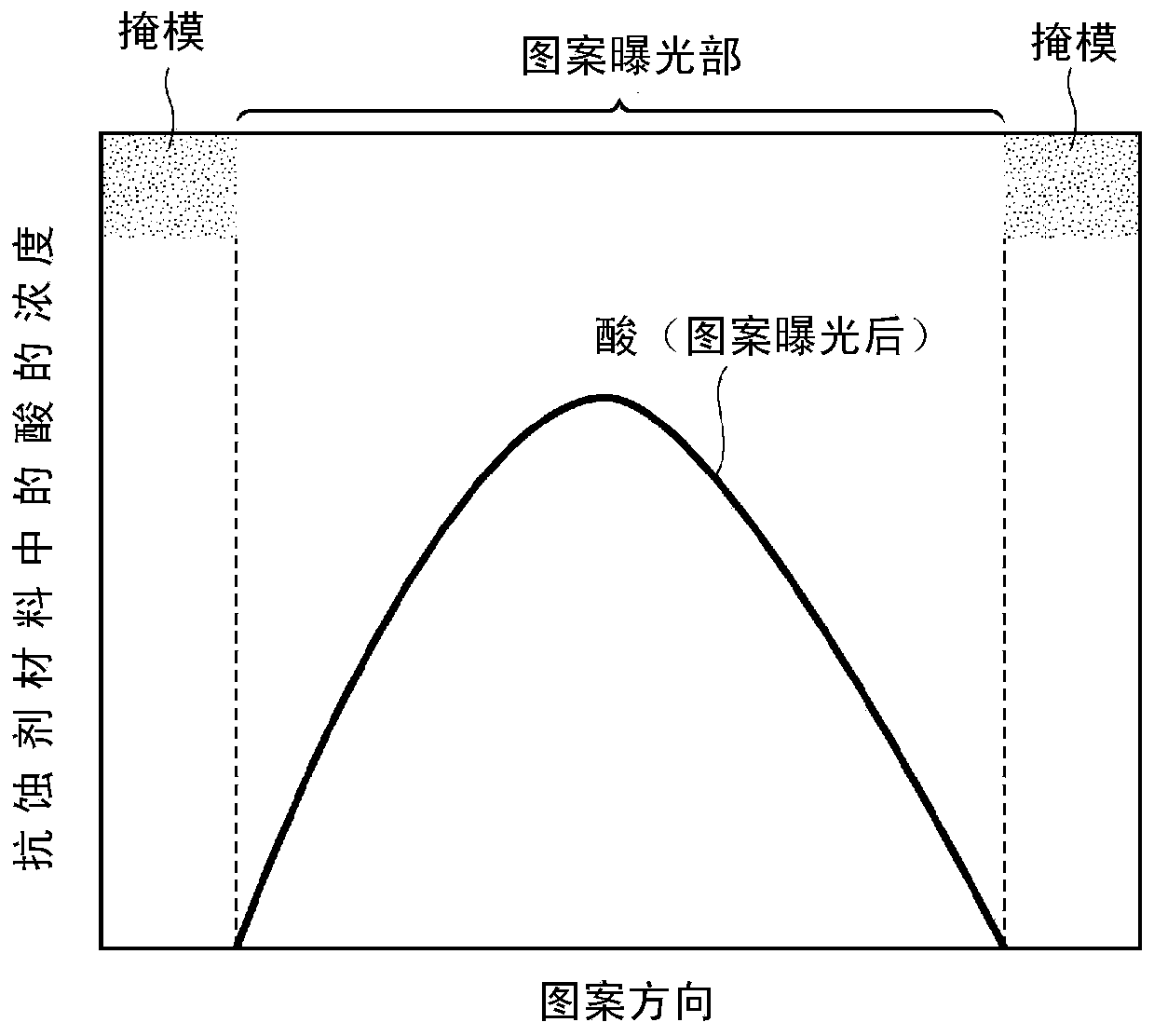
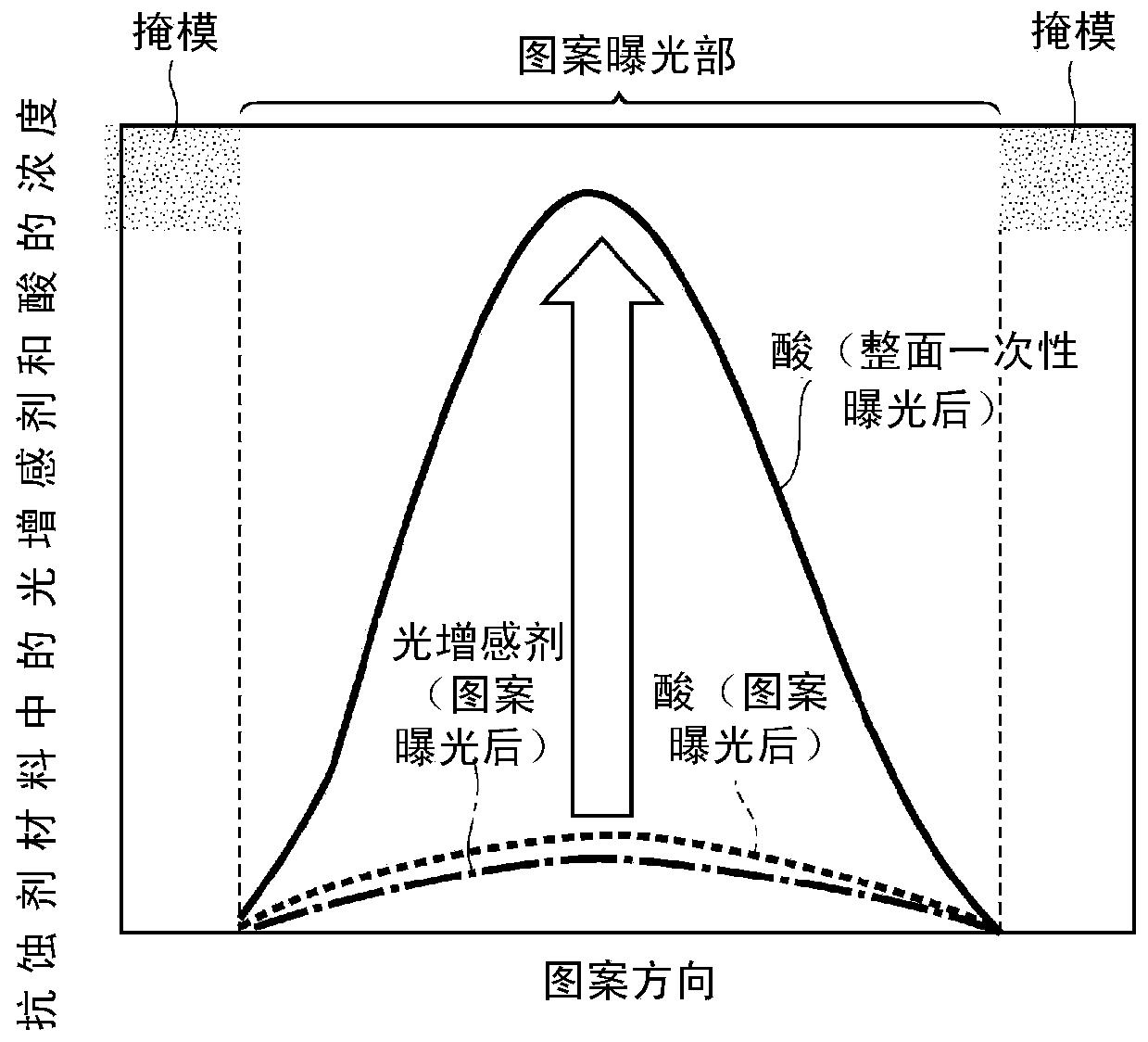
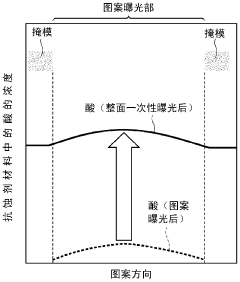
Photosensitization chemical-amplification type resist material, method for forming pattern, semiconductor device, mask for lithography, and template for nanoimprinting
PatentActiveCN111562720A
Innovation
- Photosensitized chemically amplified resist material is used. This material is exposed, baked and developed through a two-stage exposure photolithography process using ionizing radiation or non-ionizing radiation to form a resist with high sensitivity and excellent photolithography characteristics. agent pattern.
Photoresist and patterning process
PatentInactiveUS20120003582A1
Innovation
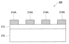
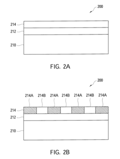
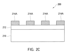
- Incorporating a luminescent agent into the photoresist coating that absorbs short-wavelength EUV light and converts it into longer-wavelength UV-Vis light, which can be absorbed by PAGs to generate acid, thereby improving acid generation efficiency and reducing heat generation.
Environmental Impact of EUV Resist Processing
The environmental footprint of EUV resist processing represents a critical consideration in semiconductor manufacturing. Chemical amplification mechanisms in EUV resists, while enabling high-resolution patterning at reduced exposure doses, introduce significant environmental challenges throughout their lifecycle. The processing of these materials involves multiple chemical-intensive steps including coating, exposure, post-exposure baking, development, and etching.
Primary environmental concerns stem from the volatile organic compounds (VOCs) released during resist application and development. Traditional EUV resist systems utilize solvents such as propylene glycol methyl ether acetate (PGMEA) and cyclohexanone, which contribute to air pollution and potential groundwater contamination when improperly managed. Additionally, the photoacid generators (PAGs) in chemically amplified resists often contain perfluorinated compounds that persist in the environment and may bioaccumulate in living organisms.
Water consumption represents another substantial environmental impact, with semiconductor manufacturing facilities utilizing millions of gallons daily for resist processing and wafer cleaning. The resulting wastewater contains complex mixtures of resist components, developers, and rinse additives that require specialized treatment before discharge.
Energy intensity further compounds the environmental footprint of EUV lithography. The EUV exposure tools themselves demand significant power, but the entire resist processing workflow—including temperature-controlled environments, post-exposure baking, and curing steps—contributes substantially to the carbon footprint of semiconductor manufacturing.
Recent industry initiatives have focused on developing more sustainable approaches to EUV resist processing. These include transitioning to water-based or bio-derived solvents, implementing closed-loop recycling systems for chemical recovery, and designing resist formulations with reduced environmental persistence. Metal-oxide resists, for instance, offer potential advantages through reduced organic content and simplified processing requirements.
Regulatory frameworks worldwide are increasingly addressing these environmental concerns. The European Union's REACH regulations and similar initiatives in Asia and North America have placed greater scrutiny on the chemical components of resist systems, driving manufacturers toward greener alternatives. Leading semiconductor companies have established ambitious sustainability targets, including zero waste to landfill policies and carbon neutrality goals that encompass their resist processing operations.
Semiconductor Industry Integration Roadmap
The integration of EUV lithography into semiconductor manufacturing represents a pivotal shift in the industry's technological trajectory. As chipmakers continue to pursue Moore's Law, the semiconductor industry roadmap increasingly relies on EUV technology to achieve sub-7nm nodes and beyond. The chemical amplification mechanisms in EUV resist materials play a critical role in this integration pathway.
Current semiconductor fabrication facilities are undergoing significant retooling to accommodate EUV lithography systems, with major investments focused on infrastructure that supports the unique requirements of EUV resist processing. This transition necessitates not only new equipment but also novel process flows that account for the distinct chemical interactions occurring within EUV resist materials.
The industry roadmap projects a phased adoption approach, with leading-edge manufacturers already implementing EUV for critical layers at 7nm and 5nm nodes. By 2023-2025, broader implementation across multiple layers is expected, with the technology becoming standard for advanced logic and memory production. This timeline aligns with the ongoing development of resist materials that can meet increasingly stringent sensitivity, resolution, and line edge roughness requirements.
Integration challenges remain significant, particularly regarding the compatibility of chemical amplification mechanisms with existing semiconductor manufacturing processes. Defectivity control, pattern collapse prevention, and resist outgassing management represent key hurdles that must be addressed through coordinated efforts between material suppliers and equipment manufacturers.
The economic implications of this integration are substantial, with initial high costs gradually offset by improved yields and increased device performance. Industry consortia such as IMEC, SEMATECH, and research partnerships between major semiconductor companies and resist suppliers are accelerating the development of standardized processes for EUV resist implementation.
Looking forward, the semiconductor industry roadmap anticipates complete integration of chemically amplified EUV resists for high-volume manufacturing by 2025, with subsequent transitions to non-CAR alternatives as pattern dimensions continue to shrink. This evolution will require continued innovation in resist chemistry, exposure tools, and metrology capabilities to maintain the industry's historical pace of advancement.
Unlock deeper insights with Patsnap Eureka Quick Research — get a full tech report to explore trends and direct your research. Try now!
Generate Your Research Report Instantly with AI Agent
Supercharge your innovation with Patsnap Eureka AI Agent Platform!