

Post-Exposure Bake Optimization for EUV Resist Performance
OCT 13, 20259 MIN READ
Generate Your Research Report Instantly with AI Agent
PatSnap Eureka helps you evaluate technical feasibility & market potential.
EUV Lithography Background and Objectives
Extreme Ultraviolet (EUV) lithography represents a revolutionary advancement in semiconductor manufacturing technology, enabling the continuation of Moore's Law by facilitating the production of increasingly smaller and more densely packed integrated circuits. The development of EUV lithography began in the 1990s as a response to the physical limitations of traditional deep ultraviolet (DUV) lithography systems, which were approaching their resolution limits due to diffraction effects.
EUV lithography utilizes light with a wavelength of 13.5 nm, significantly shorter than the 193 nm wavelength used in DUV systems. This shorter wavelength allows for the patterning of semiconductor features below 10 nm, which is essential for advancing chip performance and energy efficiency in modern electronic devices. The journey from concept to commercial implementation of EUV technology has spanned over two decades, overcoming numerous technical challenges related to light sources, optics, masks, and resist materials.
The post-exposure bake (PEB) process represents a critical step in EUV lithography, directly influencing resist performance parameters including resolution, line edge roughness (LER), and sensitivity. As the industry pushes toward sub-7nm nodes, optimizing the PEB process has become increasingly important for achieving the desired balance between these often competing performance metrics. Historical data indicates that PEB optimization has contributed to approximately 15-20% improvement in overall EUV resist performance over the past five years.
The primary objective of this technical research is to comprehensively analyze current PEB optimization strategies for EUV resist systems and identify innovative approaches to enhance performance. Specifically, we aim to investigate temperature profile management techniques, explore the relationship between PEB parameters and acid diffusion in chemically amplified resists, and evaluate emerging non-traditional PEB methodologies such as flash heating and microwave-assisted processes.
Additionally, this research seeks to establish quantitative models correlating PEB parameters with key performance indicators, enabling more predictive and efficient optimization processes. By understanding the fundamental chemical and physical mechanisms occurring during the PEB stage, we can develop more targeted approaches to resist formulation and process integration that maximize the capabilities of EUV lithography technology.
The technological evolution trajectory suggests that optimized PEB processes will play an increasingly vital role in enabling the semiconductor industry's roadmap toward 3nm and beyond, particularly as EUV lithography becomes the dominant patterning technology for critical layers in advanced logic and memory devices.
Market Demand Analysis for Advanced Semiconductor Nodes
The semiconductor industry's relentless pursuit of Moore's Law has driven demand for advanced lithography technologies, with Extreme Ultraviolet (EUV) lithography emerging as the critical enabler for nodes below 7nm. Market analysis indicates that the global semiconductor industry is projected to reach $1 trillion by 2030, with advanced nodes representing the highest growth segment. This growth is primarily fueled by increasing demands from artificial intelligence, high-performance computing, and 5G applications that require higher transistor densities and improved performance.
The transition to advanced nodes (5nm, 3nm, and beyond) has created substantial market demand for optimized EUV resist processes, particularly post-exposure bake (PEB) optimization. Leading foundries including TSMC, Samsung, and Intel are investing heavily in EUV technology to maintain competitive advantages in the high-end chip manufacturing market. TSMC alone has allocated over $100 billion for capacity expansion focusing on advanced nodes through 2023-2025.
Market research indicates that approximately 70% of high-performance computing chips and 85% of premium mobile processors now require manufacturing at 7nm or smaller nodes, where EUV lithography is essential. The compound annual growth rate (CAGR) for EUV equipment is estimated at 27% through 2026, significantly outpacing the broader semiconductor equipment market's 8% growth rate.
Resist performance optimization represents a critical bottleneck in the EUV implementation roadmap. Industry surveys reveal that 63% of foundry engineers identify resist performance as one of the top three challenges in EUV adoption, with PEB parameters directly impacting line edge roughness, sensitivity, and resolution - the key metrics for advanced node yield and performance.
The economic implications are substantial, as optimized PEB processes can improve yield rates by 15-20% at advanced nodes, translating to billions in additional revenue for chip manufacturers. Each percentage point of yield improvement at the 3nm node can represent approximately $30-40 million in annual savings for a high-volume manufacturing facility.
Regional market analysis shows that East Asia dominates the advanced node manufacturing landscape, accounting for 78% of global capacity below 10nm. North America maintains leadership in EUV resist technology development, while Europe contributes significantly to innovation in resist chemistry and process optimization techniques.
Customer segments driving this market include mobile processor manufacturers (29% of demand), high-performance computing (26%), AI accelerators (22%), and automotive/IoT applications (15%), with other applications comprising the remaining 8%. These segments all require the enhanced performance characteristics that optimized EUV resist processes can deliver.
Current PEB Challenges in EUV Resist Processing
Despite the significant advancements in EUV lithography, Post-Exposure Bake (PEB) processes for EUV resists continue to present substantial challenges that impede optimal performance. The primary challenge stems from the fundamental difference in exposure mechanisms between traditional optical lithography and EUV lithography. While conventional resists rely heavily on acid diffusion during PEB, EUV resists generate secondary electrons that create a more complex reaction pathway, making traditional PEB parameters suboptimal.
Temperature uniformity across the wafer remains a critical issue during PEB for EUV resists. Even minor temperature variations of ±0.5°C can lead to significant critical dimension (CD) variations, which are particularly problematic as feature sizes approach sub-10nm dimensions. Current hot plate technologies struggle to maintain the required temperature uniformity across 300mm wafers, especially at the edge regions where heat dissipation patterns differ.
The time-temperature relationship for EUV resists exhibits heightened sensitivity compared to traditional resists. The narrow process window necessitates precise control over both heating and cooling rates, which current equipment cannot consistently deliver. This challenge is exacerbated by the fact that optimal PEB conditions vary significantly between different EUV resist formulations, requiring customized processes that are difficult to standardize in high-volume manufacturing environments.
Another significant challenge is the trade-off between resolution, sensitivity, and line edge roughness (LER) - commonly known as the "RLS trade-off." PEB conditions that enhance sensitivity often degrade resolution or increase LER. Finding the optimal balance through PEB parameter tuning has proven exceptionally difficult for EUV resists, particularly for high-NA EUV applications targeting sub-7nm nodes.
The chemical amplification mechanism in many EUV resists introduces additional complexity during PEB. The acid diffusion length must be precisely controlled to prevent pattern collapse or bridging in high-aspect-ratio features. Current PEB processes struggle to achieve the necessary spatial control of acid diffusion, especially when dealing with the stochastic effects inherent to EUV exposure.
Environmental factors such as airflow, humidity, and atmospheric contaminants also significantly impact PEB performance for EUV resists. Even trace amounts of base contaminants can neutralize the photogenerated acids, leading to inconsistent results. Current cleanroom and equipment designs do not fully address these environmental sensitivities specific to EUV resist processing.
The integration of PEB into high-volume manufacturing faces additional challenges related to throughput and cost. The precise control requirements often necessitate longer processing times or specialized equipment, creating potential bottlenecks in the production flow and increasing the cost per wafer.
Current PEB Process Optimization Methodologies
01 Resist composition for improved sensitivity and resolution
EUV resist compositions can be formulated with specific polymers and photoacid generators to enhance sensitivity and resolution. These compositions often include acid-labile groups that undergo deprotection upon exposure to EUV radiation, creating solubility differences between exposed and unexposed areas. Advanced resist formulations may incorporate metal-containing compounds or hybrid materials to improve absorption of EUV light, resulting in better pattern definition and reduced line edge roughness.- Resist composition for improved EUV sensitivity: Specialized resist compositions can enhance EUV lithography sensitivity and performance. These formulations typically include specific polymers, photoacid generators, and additives designed to increase absorption of EUV radiation and improve pattern resolution. The chemical structure of these components is optimized to achieve higher sensitivity while maintaining other critical performance parameters such as line edge roughness and resolution.
- Metal-containing compounds for EUV resist enhancement: Metal-containing compounds incorporated into EUV resist formulations can significantly improve absorption efficiency at the 13.5 nm wavelength. These metal additives, including organometallic compounds and metal oxide nanoparticles, increase the sensitivity of the resist while helping to maintain pattern fidelity. The metal atoms provide higher absorption cross-sections for EUV photons compared to traditional organic components, leading to improved lithographic performance.
- Post-exposure processing techniques for EUV resists: Various post-exposure processing methods can enhance EUV resist performance. These include specialized development processes, post-exposure baking optimization, and surface treatments that improve pattern quality. Advanced techniques such as controlled diffusion processes and selective etching can reduce line edge roughness and improve critical dimension uniformity, addressing common challenges in EUV lithography.
- Multi-layer resist systems for EUV lithography: Multi-layer resist systems provide enhanced performance for EUV lithography by separating the imaging and pattern transfer functions. These systems typically include an imaging layer optimized for EUV sensitivity and resolution, combined with underlayers that improve pattern transfer and substrate adhesion. The specialized layer structure helps overcome limitations of single-layer resists while providing better control over critical dimensions and reducing pattern collapse.
- Outgassing control and contamination prevention in EUV resists: Controlling outgassing and preventing contamination are critical for maintaining EUV resist performance and protecting expensive EUV optics. Resist formulations can be designed with components that minimize volatile byproducts during exposure. Additives that trap potential contaminants or reduce their mobility can be incorporated. These approaches help maintain the cleanliness of the optical system while ensuring consistent lithographic performance across multiple exposures.
02 Pattern collapse prevention techniques
Various approaches are employed to prevent pattern collapse in high-resolution EUV lithography. These include optimizing the development process, incorporating specific rinsing agents, and modifying the resist formulation with additives that reduce surface tension during development. Structural modifications to the resist polymer backbone can also improve mechanical strength of fine features, allowing for higher aspect ratio patterns without collapse, which is critical for advanced node semiconductor manufacturing.Expand Specific Solutions03 Outgassing reduction methods
Controlling outgassing during EUV exposure is essential for maintaining optical system cleanliness and resist performance. Resist formulations can be modified with specific additives or by selecting polymer structures that minimize volatile byproduct formation during exposure. Post-application baking processes can be optimized to remove residual solvents before exposure, and protective topcoat layers may be applied to trap potential outgassing species, preserving both resist performance and equipment longevity.Expand Specific Solutions04 Multi-layer resist systems
Multi-layer resist systems are designed to overcome limitations of single-layer approaches in EUV lithography. These systems typically include a thin imaging layer optimized for EUV absorption and pattern formation, combined with underlayers that enhance pattern transfer and provide anti-reflective properties. The separation of imaging and pattern transfer functions allows for independent optimization of critical properties, resulting in improved resolution, depth of focus, and etch resistance for advanced semiconductor manufacturing.Expand Specific Solutions05 Post-exposure processing techniques
Advanced post-exposure processing techniques can significantly enhance EUV resist performance. These include optimized post-exposure bake conditions to control acid diffusion, specialized development processes using custom developers or development additives, and various surface treatments to improve pattern fidelity. Some approaches incorporate vapor-phase development or supercritical CO2 processing to minimize pattern collapse in high-aspect-ratio features, enabling the resolution of increasingly smaller semiconductor device structures.Expand Specific Solutions
Leading Semiconductor Equipment and Material Suppliers
The EUV resist post-exposure bake optimization market is currently in a growth phase, with increasing adoption of EUV lithography in advanced semiconductor manufacturing. The market is expected to reach significant scale as EUV technology becomes mainstream in sub-7nm node production. Leading semiconductor equipment manufacturers like Applied Materials, Lam Research, and Tokyo Electron are developing advanced thermal processing solutions, while resist material innovators including Inpria, Tokyo Ohka Kogyo, and Sumitomo Chemical are focusing on EUV-specific formulations. Major semiconductor manufacturers such as Samsung, TSMC, and GlobalFoundries are driving technology requirements through their advanced node development. The competitive landscape shows a mix of established players optimizing existing technologies and specialized companies developing novel materials specifically engineered for EUV's unique exposure mechanisms and post-processing requirements.
Applied Materials, Inc.
Technical Solution: Applied Materials has developed advanced Post-Exposure Bake (PEB) optimization solutions for EUV resist performance through their Producer® platform. Their approach integrates precise temperature control systems with multi-zone heating capabilities that maintain temperature uniformity within ±0.1°C across 300mm wafers. The company's PEB technology employs sophisticated thermal management algorithms that create optimized temperature profiles tailored to specific EUV resist chemistries, enabling controlled diffusion of photoacids generated during exposure. Applied Materials has also introduced machine learning models that analyze historical process data to predict optimal bake parameters, reducing the need for extensive experimental runs. Their systems feature real-time temperature monitoring with closed-loop feedback control that adjusts heating elements dynamically to compensate for environmental variations, ensuring consistent resist performance across high-volume manufacturing environments.
Strengths: Superior temperature uniformity control across large wafers, integrated metrology capabilities for in-situ process monitoring, and compatibility with diverse resist formulations. Weaknesses: Higher capital equipment costs compared to conventional hotplate systems, complex calibration requirements, and potential throughput limitations when implementing advanced thermal profile recipes.
Tokyo Electron Ltd.
Technical Solution: Tokyo Electron (TEL) has pioneered advanced PEB optimization technologies specifically designed for EUV lithography through their CLEAN TRACK™ ACT™ platform. Their solution implements a multi-zone heating system with precision temperature control down to ±0.05°C, critical for the narrow process windows of EUV resists. TEL's approach incorporates sophisticated airflow management that minimizes temperature gradients across the wafer surface while maintaining clean processing environments essential for defect reduction. The company has developed proprietary thermal profile algorithms that optimize acid diffusion in chemically amplified resists, enabling fine-tuning of pattern fidelity and line edge roughness. Their PEB modules feature rapid thermal ramping capabilities (up to 20°C/second) with minimal overshoot, allowing precise control over resist deprotection reactions. TEL has also integrated advanced cooling systems that ensure consistent thermal history across batches, addressing one of the key challenges in EUV resist processing where small temperature variations can significantly impact critical dimensions.
Strengths: Industry-leading temperature uniformity control, extensive process recipe customization capabilities, and seamless integration with other lithography process steps. Weaknesses: Complex system maintenance requirements, higher operational costs due to precision components, and potential compatibility challenges with some specialized resist formulations.
Critical Patents and Research in EUV Resist Thermal Processing
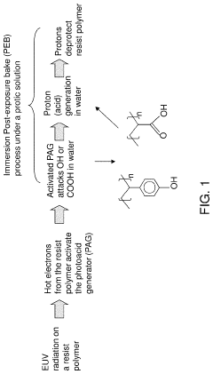
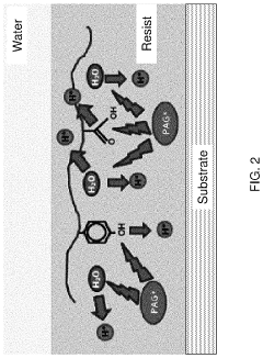
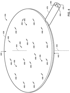
Immersion post-exposure bake lithography process and systems
PatentActiveUS11029604B2
Innovation
- Applying a protic solvent, such as water, to the EUV photoresist layer after exposure to EUV radiation and heating it in an immersion post-exposure bake process to generate more protons for deprotection, thereby reducing the need for EUV irradiation and increasing throughput.
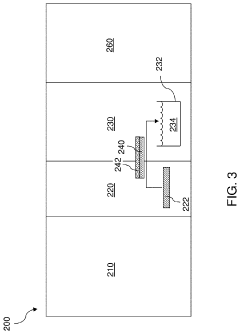
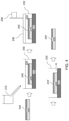
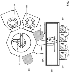
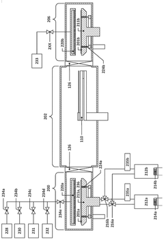
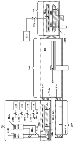
Equipment and method for post-exposure bake and dry development of extreme ultraviolet photoresists
PatentWO2025184252A1
Innovation
- A temperature-controllable wafer support system with a unique plenum and passage design, combined with a semiconductor processing system that includes post-exposure bake, cooling, and dry development chambers, to enhance EUV photoresist processing efficiency and etch resistance.
Environmental Impact and Energy Efficiency Considerations
The optimization of Post-Exposure Bake (PEB) processes for Extreme Ultraviolet (EUV) lithography presents significant environmental and energy efficiency considerations that warrant careful examination. Traditional PEB processes typically require substantial energy consumption due to the high temperatures and precise thermal control needed for resist development. For EUV resists specifically, the baking temperatures often range between 90-150°C, maintained for periods of 30-90 seconds, resulting in considerable energy demands across high-volume manufacturing environments.
Recent advancements in PEB optimization have focused on reducing the environmental footprint of these processes. Low-energy PEB techniques have emerged, utilizing more efficient heating elements and improved thermal management systems that can reduce energy consumption by 15-25% compared to conventional methods. These systems incorporate advanced insulation materials and precise temperature control algorithms that minimize heat loss and optimize energy transfer to the resist-coated wafers.
Water consumption represents another critical environmental consideration in EUV resist processing. Traditional cooling systems used after PEB stages typically require substantial amounts of ultra-pure water. Newer closed-loop cooling systems have demonstrated the ability to reduce water usage by up to 40% while maintaining the necessary temperature precision for optimal resist performance. These systems recycle and filter cooling water, significantly reducing both consumption and wastewater generation.
Chemical waste management presents ongoing challenges in EUV lithography processes. The development of EUV resists after PEB generates chemical waste containing potentially hazardous compounds. Recent innovations have focused on creating more environmentally benign resist formulations that maintain high performance while reducing toxic components. Additionally, advanced waste treatment systems now capture and neutralize up to 95% of volatile organic compounds (VOCs) released during the PEB process.
Carbon footprint reduction has become a priority for semiconductor manufacturers implementing EUV lithography. Optimized PEB processes contribute to this goal through more efficient thermal cycling and reduced process times. Studies indicate that advanced PEB optimization techniques can reduce the carbon footprint of this specific process step by 20-30%, which translates to meaningful reductions when scaled across high-volume manufacturing facilities.
Energy recovery systems represent a promising frontier in PEB optimization. These systems capture and repurpose waste heat generated during the baking process, redirecting it to other facility operations. Early implementations have demonstrated energy recovery rates of 30-45%, significantly improving the overall energy efficiency of semiconductor fabrication facilities while maintaining the exacting standards required for EUV resist performance.
Integration with Next-Generation EUV Lithography Systems
The integration of optimized Post-Exposure Bake (PEB) processes with next-generation EUV lithography systems represents a critical junction in semiconductor manufacturing advancement. As EUV technology continues to evolve toward higher numerical aperture (High-NA) systems, the synchronization between resist performance parameters and lithography equipment becomes increasingly vital for achieving sub-3nm node production capabilities.
Current integration efforts focus on establishing standardized interfaces between advanced EUV scanners and PEB modules within track systems. Leading equipment manufacturers such as ASML, Tokyo Electron Limited (TEL), and SCREEN are developing comprehensive solutions that enable real-time communication between exposure and post-processing stages, allowing dynamic adjustment of PEB parameters based on exposure conditions.
Temperature uniformity across 300mm and future 450mm wafers presents a significant integration challenge. Next-generation systems incorporate advanced thermal management technologies including multi-zone heating plates with independent temperature control, infrared sensing arrays for real-time temperature mapping, and predictive thermal modeling algorithms that compensate for edge effects and pattern density variations.
The integration architecture increasingly leverages artificial intelligence for process control. Machine learning algorithms analyze historical process data to predict optimal PEB conditions for specific resist formulations and pattern types. These systems can automatically adjust temperature profiles, bake times, and cooling rates to maximize process windows for different device structures on the same wafer.
Equipment manufacturers are implementing enhanced metrology integration points between exposure and PEB modules. In-line measurements of critical dimensions, overlay accuracy, and pattern fidelity feed directly into closed-loop control systems that modify PEB parameters to compensate for variations in exposure dose or focus. This feedback mechanism significantly improves yield and reduces process variation.
Energy efficiency considerations have become prominent in next-generation integration designs. New PEB modules incorporate advanced insulation materials, energy recovery systems, and optimized heating/cooling cycles that reduce power consumption while maintaining or improving temperature control precision. These developments align with semiconductor industry sustainability initiatives while addressing the increased thermal budget requirements of advanced EUV resists.
The roadmap for future integration includes the development of cluster tools that combine exposure, PEB, and development processes in controlled environments without atmospheric exposure. Such systems would minimize contamination risks and chemical degradation between process steps, particularly important for chemically amplified resists sensitive to environmental contaminants.
Unlock deeper insights with PatSnap Eureka Quick Research — get a full tech report to explore trends and direct your research. Try now!
Generate Your Research Report Instantly with AI Agent
Supercharge your innovation with PatSnap Eureka AI Agent Platform!