Resist Chemistry Adaptation for High-NA EUV Lithography
OCT 13, 20259 MIN READ
Generate Your Research Report Instantly with AI Agent
Patsnap Eureka helps you evaluate technical feasibility & market potential.
High-NA EUV Lithography Resist Evolution and Objectives
Extreme Ultraviolet (EUV) lithography has emerged as a transformative technology in semiconductor manufacturing, enabling the continuation of Moore's Law through increasingly smaller feature sizes. The evolution toward High-NA (Numerical Aperture) EUV represents the next significant advancement in this field, promising to extend resolution capabilities beyond current limits. The journey of EUV lithography began in the early 2000s with research initiatives, followed by the introduction of 0.33 NA EUV scanners in commercial production around 2018-2019, marking a pivotal shift from traditional 193nm immersion lithography.
High-NA EUV lithography, with its numerical aperture increased from 0.33 to 0.55, theoretically enables resolution improvements of approximately 70%, potentially supporting feature sizes below 8nm. This technological leap necessitates fundamental adaptations in resist chemistry to accommodate the steeper angles of incidence and increased photon energy density characteristic of High-NA systems.
The historical progression of resist materials for lithography has seen transitions from DNQ-Novolac resists to chemically amplified resists (CARs), and now toward novel non-CAR alternatives specifically engineered for EUV applications. Each generation has addressed specific challenges related to resolution, sensitivity, and line edge roughness (LER) – the so-called "triangle of death" in resist performance metrics.
Current objectives in High-NA EUV resist development focus on several critical parameters. First, achieving enhanced resolution capabilities below 8nm half-pitch while maintaining pattern fidelity. Second, improving sensitivity to reduce exposure times and increase throughput, with targets of <20mJ/cm² for economically viable production. Third, minimizing LER to below 2nm to ensure electrical performance and yield in advanced node devices.
Additionally, resist materials must demonstrate compatibility with increasingly complex multi-patterning schemes and be engineered to withstand the higher energy density of High-NA systems without degradation. Material stability under vacuum conditions and resistance to outgassing represent further technical requirements specific to EUV environments.
The industry roadmap anticipates High-NA EUV implementation in high-volume manufacturing by 2025-2026, necessitating accelerated development cycles for resist chemistry. This timeline creates urgency for fundamental innovations in molecular design, photochemical mechanisms, and process integration methodologies.
Collaborative ecosystems involving material suppliers, equipment manufacturers, and semiconductor companies have formed to address these challenges collectively, recognizing that resist chemistry adaptation represents one of the critical enablers for realizing the full potential of High-NA EUV technology in advancing semiconductor manufacturing capabilities.
Market Analysis for Advanced Semiconductor Lithography Solutions
The advanced semiconductor lithography market is experiencing a significant transformation with the introduction of High-NA EUV technology. The global semiconductor lithography equipment market is currently valued at approximately $16 billion, with projections indicating growth to $25 billion by 2027, representing a compound annual growth rate of 9.3%. EUV lithography systems specifically account for nearly 35% of this market value, despite representing a smaller percentage of unit sales due to their high cost per system.
High-NA EUV lithography represents the next evolutionary step beyond standard EUV technology, with market adoption expected to accelerate from 2025 onwards. Early adopters include leading semiconductor manufacturers focused on sub-3nm process nodes, with Taiwan, South Korea, and the United States serving as primary markets. The specialized resist chemistry required for High-NA EUV is projected to create a distinct sub-segment within the photoresist market, estimated to reach $500 million annually by 2028.
Customer demand is primarily driven by the need for continued miniaturization in logic and memory applications. Logic manufacturers require High-NA EUV solutions to enable the 2nm node and beyond, while memory manufacturers seek higher density DRAM and advanced 3D NAND structures. The market demonstrates strong willingness to invest in these advanced solutions despite capital costs exceeding $300 million per High-NA EUV system.
Regional market analysis reveals Asia-Pacific dominates demand with approximately 70% market share, led by Taiwan and South Korea. North America accounts for 20% of the market, primarily driven by leading U.S. semiconductor manufacturers, while Europe represents about 10%, focused on research and specialized applications.
The resist chemistry adaptation market specifically shows promising growth potential, with specialized chemical suppliers positioned to capture significant value. Current market leaders include JSR Corporation, Tokyo Ohka Kogyo, and Shin-Etsu Chemical, collectively controlling over 75% of the advanced photoresist market. New entrants focused exclusively on High-NA EUV resist solutions are emerging, particularly from venture-backed startups in the U.S. and Japan.
Customer pain points center around three key areas: resist sensitivity requirements that balance throughput with pattern fidelity, line edge roughness control at increasingly smaller dimensions, and integration challenges with existing manufacturing processes. Market research indicates customers are willing to pay premium prices for resist solutions that effectively address these challenges, with price sensitivity decreasing as technical performance increases.
The total addressable market for High-NA EUV resist chemistry is expected to grow at 15% annually through 2030, outpacing the broader semiconductor materials market, as manufacturers transition to more advanced nodes requiring specialized materials solutions.
Current Resist Chemistry Challenges in High-NA EUV Implementation
The implementation of High-NA EUV lithography presents significant challenges for resist chemistry, requiring substantial adaptations to meet the demands of this advanced technology. Current resist materials face several critical limitations when transitioning to High-NA EUV systems. The increased numerical aperture (NA) from 0.33 to 0.55 necessitates resists capable of resolving features below 8nm half-pitch, pushing chemical formulations beyond their current capabilities.
One primary challenge is the photon absorption efficiency. High-NA EUV systems operate at the same 13.5nm wavelength as standard EUV, but the higher NA value results in reduced depth of focus. This requires thinner resist films (typically <30nm) while maintaining sufficient EUV photon absorption. Current chemically amplified resists (CARs) struggle to achieve adequate sensitivity at these reduced thicknesses, leading to pattern collapse and line edge roughness issues.
Stochastic effects represent another significant barrier. At the extreme dimensions targeted by High-NA EUV, random variations in photon absorption, acid diffusion, and molecular distribution become increasingly problematic. These stochastic effects manifest as shot noise, resulting in line edge roughness, line width roughness, and defectivity that can compromise pattern fidelity. Current resist platforms lack sufficient mechanisms to mitigate these statistical variations.
Resolution capabilities of existing resists also fall short of High-NA EUV requirements. While leading-edge resists can achieve approximately 13nm resolution in standard EUV systems, High-NA EUV targets sub-8nm features. The resolution-sensitivity-line edge roughness (RLS) trade-off becomes even more pronounced, with current chemistries unable to simultaneously satisfy all three parameters at High-NA dimensions.
Pattern collapse presents a formidable challenge as aspect ratios increase with smaller features. Surface tension forces during development and rinse processes cause mechanical failure in high-aspect-ratio structures. Current resist formulations lack the mechanical strength and adhesion properties necessary to withstand these forces at High-NA dimensions.
Additionally, outgassing characteristics of existing resists pose contamination risks to the sophisticated High-NA EUV optics. The vacuum environment of EUV systems makes them particularly vulnerable to molecular contamination from resist components, requiring new formulations with minimal outgassing properties.
The acid diffusion control mechanisms in current CARs are insufficient for High-NA applications. The diffusion length of photogenerated acids must be precisely controlled to prevent feature blurring while maintaining sensitivity, a balance not achievable with existing quencher systems and polymer platforms.
Existing Resist Chemistry Adaptation Approaches for High-NA EUV
01 Photoresist composition optimization
Optimization of photoresist compositions involves adjusting chemical formulations to enhance lithographic performance. This includes modifying polymers, photoactive compounds, and additives to improve resolution, sensitivity, and pattern fidelity. Advanced resist chemistry adaptations focus on achieving finer feature sizes while maintaining process stability across various exposure conditions.- Photoresist composition optimization: Optimization of photoresist compositions involves modifying chemical formulations to enhance performance characteristics such as sensitivity, resolution, and pattern fidelity. This includes adjusting polymer structures, photoactive compounds, and additives to achieve desired lithographic properties. Advanced resist chemistry adaptations enable improved line edge roughness, better adhesion to substrates, and increased resistance to etching processes, which are critical for semiconductor manufacturing.
- Process parameter adjustment for resist performance: Adapting resist chemistry often requires corresponding adjustments to process parameters such as exposure conditions, development time, and baking temperatures. These adjustments are essential to accommodate changes in resist formulation and to optimize the overall lithographic process. Simulation tools and modeling techniques can be used to predict how resist will behave under different processing conditions, allowing for efficient adaptation of resist chemistry to specific manufacturing requirements.
- Resist chemistry for advanced semiconductor applications: Specialized resist chemistry adaptations are developed for advanced semiconductor manufacturing processes, including extreme ultraviolet (EUV) lithography and multi-patterning techniques. These adaptations focus on creating resist materials with high sensitivity to specific wavelengths of light, improved resolution capabilities, and compatibility with complex process flows. Chemical modifications to resist formulations enable the creation of smaller feature sizes and more complex circuit patterns required for cutting-edge semiconductor devices.
- Environmental and safety considerations in resist chemistry: Modern resist chemistry adaptation increasingly focuses on developing more environmentally friendly and safer formulations. This includes reducing or eliminating hazardous solvents, implementing water-based resist systems, and creating biodegradable components. These adaptations aim to minimize environmental impact and improve workplace safety while maintaining or enhancing the technical performance of the resist materials for various lithographic applications.
- Computational methods for resist chemistry optimization: Advanced computational techniques are employed to accelerate the development and adaptation of resist chemistry. These methods include machine learning algorithms, molecular modeling, and quantum chemical calculations to predict resist behavior and optimize formulations. Computational approaches enable rapid screening of potential resist compositions, reducing the need for extensive experimental testing and accelerating the development of new resist materials tailored to specific lithographic requirements.
02 Process parameter adjustment for resist performance
Adapting resist chemistry often requires corresponding adjustments to process parameters such as baking temperatures, development conditions, and exposure settings. These adjustments are critical for optimizing resist performance across different substrates and lithography tools. Computational models can be used to predict optimal process conditions for specific resist formulations.Expand Specific Solutions03 Resist adaptation for advanced semiconductor manufacturing
Specialized resist chemistry adaptations are developed for advanced semiconductor manufacturing processes, including EUV lithography, multi-patterning techniques, and 3D structures. These adaptations focus on meeting the stringent requirements of next-generation devices while addressing challenges such as line edge roughness and pattern collapse at smaller feature sizes.Expand Specific Solutions04 Computational methods for resist chemistry optimization
Computational approaches including machine learning, simulation, and modeling are increasingly used to predict resist behavior and optimize formulations. These methods accelerate the development cycle by reducing experimental iterations and enabling more precise tuning of resist properties for specific applications. Virtual screening of chemical compounds helps identify promising candidates for resist formulations.Expand Specific Solutions05 Environmental and safety considerations in resist adaptation
Modern resist chemistry adaptation increasingly focuses on developing environmentally friendly formulations with reduced toxicity and waste generation. This includes replacing harmful solvents with safer alternatives, reducing metal content, and designing processes that consume less energy and chemicals. These adaptations aim to maintain high performance while meeting stringent environmental regulations and sustainability goals.Expand Specific Solutions
Leading Semiconductor and Chemical Companies in High-NA EUV
High-NA EUV lithography resist chemistry adaptation is currently in an early growth phase, with the market poised for significant expansion as semiconductor manufacturers transition to next-generation technologies. The global market is projected to grow substantially as high-NA EUV systems begin deployment in 2024-2025. The competitive landscape features established chemical suppliers like Tokyo Ohka Kogyo, JSR Corp, and Shin-Etsu Chemical leading resist development, while equipment manufacturers including ASML, Tokyo Electron, and Applied Materials provide the enabling lithography platforms. Technical challenges remain in developing resists with sufficient sensitivity, resolution, and line edge roughness for high-NA EUV requirements. Research collaborations between industry leaders like IBM, Intel, TSMC and academic institutions are accelerating technology maturation, though commercial-scale production solutions are still evolving toward full implementation readiness.
TOKYO OHKA KOGYO CO., LTD.
Technical Solution: Tokyo Ohka Kogyo (TOK) has developed specialized resist formulations specifically engineered for High-NA EUV lithography applications. Their approach focuses on metal-containing resist systems that offer significantly higher sensitivity and absorption efficiency compared to traditional organic resists. TOK's metal oxide resist technology incorporates hafnium and zirconium compounds to enhance EUV absorption cross-sections while maintaining the resolution capabilities needed for sub-10nm features. Their proprietary resist platform includes carefully designed polymer matrices with optimized acid generators and quenchers to control diffusion lengths at the reduced depth of focus inherent to High-NA systems. TOK has also pioneered thin-film resist technologies (below 30nm thickness) that address the depth of focus challenges in High-NA EUV while maintaining sufficient etch resistance through silicon-containing components. Their development process includes extensive testing with actual High-NA exposure conditions through partnerships with tool manufacturers.
Strengths: Industry-leading expertise in metal-containing resist formulations; proven track record in EUV resist development; strong relationships with equipment manufacturers for testing and validation. Weaknesses: Higher material costs compared to traditional resists; potential for metal contamination requiring additional process steps; complex integration with existing semiconductor manufacturing processes.
JSR Corp.
Technical Solution: JSR Corporation has developed a comprehensive High-NA EUV resist platform centered around their advanced molecular design approach. Their technology focuses on precisely engineered polymer structures with optimized protecting groups that enable controlled deprotection reactions under High-NA EUV exposure conditions. JSR's resist chemistry incorporates specialized photoacid generators (PAGs) with carefully tuned diffusion characteristics to address the reduced depth of focus in High-NA systems while maintaining high resolution capability. Their formulations feature proprietary quencher compounds that help control acid diffusion and improve line edge roughness performance. JSR has pioneered multi-layer resist systems specifically for High-NA applications, where thin imaging layers work in conjunction with transfer layers to achieve both high resolution and sufficient etch resistance. The company has also developed specialized rinse materials and post-exposure bake optimization techniques that enhance pattern fidelity at the extreme dimensions required for High-NA EUV lithography.
Strengths: Extensive experience in resist chemistry formulation; strong R&D capabilities in molecular design; established relationships with major semiconductor manufacturers. Weaknesses: Challenges in balancing sensitivity and resolution requirements; complex process integration needs; high development costs for specialized materials.
Critical Patents and Innovations in High-NA EUV Resist Technology
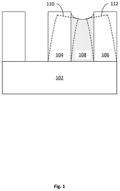
Semiconductor pattern structure preservation
PatentPendingUS20250201559A1
Innovation
- A method involving the deposition of a metal oxide resist layer, formation of pattern structures, application of a treatment composition with polymeric compounds, and tethering these compounds to the pattern structures to prevent collapse or distortion.
Mask Stitching for Extreme Ultraviolet Lithography
PatentPendingUS20250199397A1
Innovation
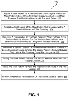
- The method involves determining locations within the mask pattern to place assistive features that reduce sensitivity to lithographic process variations and stray light at the boundary during mask exposures. These assistive features are strategically placed to mitigate the effects of double exposure in the boundary region.
Environmental Impact Assessment of Advanced Resist Materials
The environmental impact of advanced resist materials for High-NA EUV lithography represents a critical consideration in semiconductor manufacturing sustainability. These specialized photoresists contain complex chemical compounds including metal-organic clusters, fluorinated polymers, and photoacid generators that pose unique environmental challenges throughout their lifecycle.
Production of advanced EUV resists involves energy-intensive processes and hazardous precursors. Metal-organic resists containing elements like tin, antimony, or hafnium require specialized extraction and refinement methods that generate significant carbon emissions. The synthesis of fluorinated components, essential for etch resistance, produces perfluorinated compounds with high global warming potential and environmental persistence.
Waste management presents substantial challenges as EUV resist processing generates contaminated solvents, developer solutions, and rinse water containing trace metals and organic compounds. Current treatment systems struggle to completely remove these novel contaminants before discharge. Particularly concerning are metal-containing nanoparticles that may bypass conventional filtration systems and enter aquatic ecosystems, where bioaccumulation potential remains poorly understood.
Regulatory frameworks worldwide are evolving to address these emerging materials. The European Union's REACH regulation has placed increasing scrutiny on perfluorinated compounds in manufacturing processes, while semiconductor fabs in water-stressed regions face stricter effluent limitations. These regulatory pressures are driving innovation in greener resist formulations and closed-loop processing systems.
Industry initiatives show promising developments in environmental mitigation. Several leading resist manufacturers have implemented solvent recovery systems that reclaim up to 85% of process chemicals. Advanced oxidation techniques combined with specialized metal chelation systems have demonstrated improved removal efficiency for metal-organic compounds from wastewater streams. Additionally, research into bio-based polymer platforms offers potential alternatives to petroleum-derived resist components.
Life cycle assessment studies indicate that while EUV lithography offers energy efficiency advantages in device operation through enabling smaller transistors, these benefits must be balanced against the environmental footprint of more complex resist materials. The semiconductor industry faces a critical challenge in developing resist chemistries that maintain the exceptional resolution required for High-NA EUV while reducing environmental impact throughout the material lifecycle.
Supply Chain Security for Critical EUV Resist Components
The security of the EUV resist supply chain has become increasingly critical as High-NA EUV lithography advances toward commercial implementation. With only a handful of suppliers globally capable of producing the specialized chemical components required for High-NA EUV resists, the industry faces significant vulnerability to supply disruptions. These specialized materials, including photoacid generators (PAGs), quenchers, and polymer matrices, require precise manufacturing processes with extremely low contamination tolerances measured in parts per trillion.
Current supply chain structures reveal concerning geographic concentrations, with Japan dominating the production of key resist components, followed by Germany and the United States. This concentration creates potential single points of failure that could impact the entire semiconductor manufacturing ecosystem. Recent pandemic-related disruptions have highlighted these vulnerabilities, with several major semiconductor manufacturers reporting delays due to resist component shortages.
Regulatory frameworks further complicate the supply landscape, as many critical chemicals face increasing restrictions under environmental and safety regulations in various jurisdictions. Export controls on advanced materials, particularly between regions with geopolitical tensions, add another layer of complexity to securing consistent supply channels for High-NA EUV resist components.
Industry leaders have begun implementing multi-sourcing strategies, though the specialized nature of these materials limits the effectiveness of such approaches. Companies like JSR, TOK, and Shin-Etsu have invested in redundant manufacturing capabilities across different geographic regions, while semiconductor giants such as TSMC and Samsung have established strategic stockpiles of critical resist components.
Emerging technologies for on-site purification and recycling of resist materials show promise for reducing supply chain dependencies. Advanced analytical techniques for qualifying alternative suppliers have also gained traction, with organizations developing standardized protocols for rapid validation of substitute materials when primary sources become unavailable.
Long-term security strategies include vertical integration efforts, with some major semiconductor manufacturers investing in joint ventures with chemical suppliers to ensure prioritized access to critical components. International consortia focused on supply chain resilience have formed, creating shared risk mitigation frameworks and early warning systems for potential disruptions in the EUV resist supply ecosystem.
The development of alternative resist chemistries with more readily available components represents another strategic direction, though these must still meet the exacting performance requirements of High-NA EUV lithography. Research into metal-oxide resists and other novel formulations may eventually reduce dependence on the most supply-constrained components while potentially offering improved lithographic performance.
Unlock deeper insights with Patsnap Eureka Quick Research — get a full tech report to explore trends and direct your research. Try now!
Generate Your Research Report Instantly with AI Agent
Supercharge your innovation with Patsnap Eureka AI Agent Platform!