Evaluation of EUV Absorption and Quantum Efficiency in Resists
OCT 13, 20259 MIN READ
Generate Your Research Report Instantly with AI Agent
Patsnap Eureka helps you evaluate technical feasibility & market potential.
EUV Resist Technology Background and Objectives
Extreme Ultraviolet (EUV) lithography represents a revolutionary advancement in semiconductor manufacturing, enabling the continuation of Moore's Law by facilitating the production of increasingly smaller transistors. The technology utilizes 13.5 nm wavelength light to pattern semiconductor wafers, significantly improving resolution compared to traditional deep ultraviolet (DUV) lithography methods. Since its conceptualization in the 1980s, EUV lithography has evolved from theoretical possibility to commercial reality, with major milestones including the development of reliable EUV light sources and compatible resist materials.
The evolution of EUV resist technology has been particularly challenging due to the unique photochemical interactions at such short wavelengths. Traditional chemically amplified resists (CARs) that performed adequately for DUV applications have proven insufficient for EUV requirements, necessitating fundamental innovations in resist chemistry. The absorption mechanisms and quantum efficiency of resists under EUV exposure differ significantly from those observed with longer wavelengths, requiring specialized molecular designs and novel photochemical pathways.
Current technological trends point toward metal-containing resists, particularly those incorporating hafnium, zirconium, and tin, which demonstrate superior EUV absorption characteristics. Simultaneously, non-chemically amplified resists (non-CARs) have gained attention for their potential to overcome resolution limitations and reduce line edge roughness. The industry is witnessing a convergence of inorganic chemistry principles with traditional polymer science to create hybrid materials optimized for EUV absorption.
The primary technical objectives in EUV resist development center on achieving the optimal balance between sensitivity, resolution, and line edge roughness—often referred to as the "triangle trade-off." Specifically, the industry aims to develop resists capable of resolving features below 10 nm with sensitivity better than 20 mJ/cm² while maintaining acceptable line edge roughness below 2 nm (3σ). Understanding and enhancing quantum efficiency—the number of chemical events per absorbed photon—remains crucial to achieving these targets.
Additionally, the evaluation of EUV absorption mechanisms seeks to elucidate the complex cascade of events following photon absorption, including photoelectron generation, secondary electron formation, and subsequent chemical reactions. This understanding is essential for rational resist design rather than empirical optimization. The ultimate goal extends beyond performance metrics to include practical considerations such as manufacturing scalability, integration compatibility, and environmental sustainability of next-generation EUV resist platforms.
Market Analysis for EUV Lithography Materials
The global market for EUV lithography materials, particularly photoresists, has experienced significant growth driven by the semiconductor industry's push toward smaller node sizes. As of 2023, the EUV lithography materials market is valued at approximately $1.2 billion, with projections indicating a compound annual growth rate (CAGR) of 15-18% through 2028. This growth trajectory is primarily fueled by the increasing adoption of EUV technology in high-volume manufacturing by leading semiconductor companies.
The demand for EUV-specific resists is concentrated in advanced semiconductor manufacturing regions, with East Asia (particularly Taiwan, South Korea, and Japan) accounting for over 65% of the global market share. North America and Europe represent smaller but technologically significant markets, with approximately 20% and 15% market share respectively.
Key market drivers include the continuous miniaturization of semiconductor devices, with leading foundries transitioning to 5nm, 3nm, and soon 2nm process nodes. EUV lithography has become essential for these advanced nodes, creating sustained demand for high-performance resists with superior absorption characteristics and quantum efficiency.
Customer segments in this market include integrated device manufacturers (IDMs), pure-play foundries, and memory manufacturers. The foundry segment currently dominates consumption, representing approximately 55% of the total market, followed by memory manufacturers at 30% and IDMs at 15%.
Market challenges include the high cost of EUV resist materials, which can be 3-5 times more expensive than traditional ArF resists, creating pressure on manufacturers to optimize material utilization. Additionally, technical requirements for EUV resists are becoming increasingly stringent, with customers demanding higher sensitivity, lower line edge roughness, and improved pattern collapse resistance.
The competitive landscape features specialized chemical suppliers like JSR Corporation, TOK, Shin-Etsu Chemical, and DuPont, who collectively control over 75% of the EUV resist market. Recent market trends show increased R&D investments in metal-oxide resists and hybrid organic-inorganic formulations that promise better absorption characteristics and quantum efficiency.
From a regional perspective, the Asia-Pacific region is expected to maintain its dominant position, with China making significant investments to develop domestic EUV resist capabilities as part of its semiconductor self-sufficiency initiatives. North America and Europe continue to focus on innovation and specialized applications, particularly for advanced logic devices.
Current Challenges in EUV Resist Performance
Despite significant advancements in EUV lithography technology, resist performance remains a critical bottleneck in the semiconductor manufacturing process. Current EUV resists face several fundamental challenges that limit their industrial application and efficiency. The primary issue is the inherent trade-off between sensitivity, resolution, and line edge roughness (LER) - commonly known as the "RLS triangle." As resolution requirements push below 10nm, achieving adequate sensitivity while maintaining acceptable LER becomes increasingly difficult.
Sensitivity challenges are particularly pronounced due to the limited source power of EUV scanners. Current resists require approximately 20-30 mJ/cm² exposure dose, which significantly impacts throughput in production environments. The quantum efficiency of photon absorption and subsequent chemical amplification processes remains suboptimal, with only a fraction of incident photons effectively contributing to pattern formation.
Chemical amplification mechanisms, while successful for traditional lithography, present unique challenges in EUV applications. The stochastic effects become dominant at the molecular level when working with such high-energy photons (13.5nm wavelength). This results in shot noise issues and pattern variability that fundamentally limits achievable resolution and uniformity.
Material composition presents another significant challenge. Traditional chemically amplified resists (CARs) suffer from acid diffusion limitations, while metal-oxide resists face integration challenges despite their promising absorption characteristics. The incorporation of metal elements to enhance EUV absorption often introduces new complications in terms of pattern development, etching selectivity, and potential contamination concerns.
Outgassing during exposure represents a serious concern for scanner optics longevity. Current resist formulations release volatile compounds under EUV radiation that can contaminate the highly sensitive mirror systems, requiring additional protective measures that further complicate the exposure process.
Measurement and characterization methodologies for EUV resists remain inadequate. Accurately quantifying quantum efficiency, chemical reaction pathways, and absorption coefficients at the EUV wavelength requires specialized equipment and techniques that are not widely available or standardized across the industry.
The environmental stability of high-performance EUV resists also presents challenges, with many formulations showing sensitivity to ambient conditions that affects shelf life and process repeatability. This necessitates stringent storage and handling protocols that add complexity to manufacturing workflows.
Addressing these interconnected challenges requires a multidisciplinary approach combining materials science, physical chemistry, and advanced metrology to develop next-generation resist platforms capable of meeting the demanding requirements of sub-10nm semiconductor manufacturing nodes.
Existing Methodologies for EUV Absorption Measurement
01 EUV resist materials with reduced absorption
Specialized resist materials can be formulated to minimize EUV absorption while maintaining sensitivity. These materials often incorporate elements with low absorption cross-sections for EUV wavelengths. By reducing absorption in non-photochemically productive ways, more photons are available for the desired chemical reactions, improving quantum efficiency. These formulations may include specific polymers and photoacid generators designed to optimize the balance between absorption and sensitivity.- EUV resist materials with reduced absorption: Specialized resist materials can be formulated to minimize EUV absorption while maintaining sensitivity. These materials often incorporate elements with lower absorption cross-sections for EUV wavelengths. By reducing absorption in non-productive pathways, more photons can participate in the desired photochemical reactions, improving overall efficiency. These materials may include metal-free compounds or specifically designed polymers that balance transparency with reactivity.
- Quantum efficiency enhancement techniques: Various methods can be employed to enhance the quantum efficiency of EUV resist systems. These include incorporating secondary electron generators, optimizing acid generator concentration, and using sensitizers that improve the yield of photochemical reactions. By increasing the number of chemical events per absorbed photon, these techniques help overcome the inherent quantum limitations of EUV lithography processes, resulting in higher sensitivity resists with improved performance characteristics.
- Multi-layer resist structures for EUV applications: Multi-layer resist structures can be designed to optimize both absorption and quantum efficiency in EUV lithography. These structures typically include a thin imaging layer with high quantum efficiency on top of materials that manage reflection and absorption. This approach allows for fine-tuning of the overall optical properties while maintaining high resolution and sensitivity. The interfaces between layers can also be engineered to enhance performance through mechanisms like acid diffusion control.
- Measurement and modeling of EUV absorption characteristics: Advanced measurement techniques and computational models have been developed to accurately characterize EUV absorption and quantum efficiency in resist materials. These methods include spectroscopic analysis, electron yield measurements, and simulation of radiation-matter interactions at the atomic level. By providing detailed understanding of how EUV photons interact with resist components, these approaches enable rational design of materials with optimized absorption profiles and improved quantum yields.
- Novel additives for controlling EUV absorption and sensitivity: Specialized additives can be incorporated into resist formulations to modulate EUV absorption and enhance quantum efficiency. These include quenchers that prevent unwanted reactions, sensitizers that improve photon utilization, and compounds that facilitate electron transfer processes. By carefully selecting and optimizing these additives, resist developers can achieve the delicate balance between sufficient absorption for pattern formation and excessive absorption that reduces efficiency and resolution.
02 Multilayer resist systems for EUV lithography
Multilayer resist systems can be designed to manage EUV absorption and enhance quantum efficiency. These systems typically consist of different functional layers, each optimized for specific aspects of the lithographic process. The top layer may be designed for optimal EUV interaction, while underlying layers provide additional functionality such as pattern transfer or etch resistance. This approach allows for better control of absorption characteristics while maintaining high resolution and sensitivity.Expand Specific Solutions03 Quantum efficiency enhancement through sensitizers
Sensitizers can be incorporated into resist formulations to enhance quantum efficiency under EUV exposure. These compounds are designed to efficiently absorb EUV radiation and transfer energy to initiate the desired photochemical reactions. By improving the efficiency of this energy transfer process, fewer photons are needed to achieve the same lithographic result. Various types of sensitizers, including metal-based compounds and organic molecules, can be used depending on the specific resist chemistry.Expand Specific Solutions04 Measurement and modeling of EUV absorption characteristics
Advanced measurement techniques and computational models can be used to characterize and predict EUV absorption and quantum efficiency in resist materials. These methods enable the optimization of resist formulations by providing detailed information about how different components interact with EUV radiation. Techniques such as spectroscopy, scatterometry, and quantum mechanical simulations help in understanding the fundamental mechanisms of EUV absorption and energy transfer, leading to more efficient resist designs.Expand Specific Solutions05 Novel chemical structures for improved EUV performance
Novel chemical structures can be designed specifically to address the challenges of EUV absorption and quantum efficiency. These structures may include non-traditional polymer backbones, innovative protecting groups, or unique photoacid generators that respond efficiently to EUV radiation. By fundamentally rethinking the chemical architecture of resist materials, significant improvements in both absorption characteristics and quantum efficiency can be achieved, leading to better resolution, sensitivity, and line edge roughness in EUV lithography.Expand Specific Solutions
Leading Companies in EUV Resist Development
The EUV absorption and quantum efficiency in resists market is currently in a growth phase, with increasing adoption of EUV lithography in advanced semiconductor manufacturing. The global market is estimated to reach several billion dollars by 2025, driven by the semiconductor industry's push toward smaller node technologies. Leading players include ASML as the dominant EUV equipment supplier, while resist manufacturers like JSR, Tokyo Ohka Kogyo, and FUJIFILM compete in developing high-performance EUV resist materials. Major semiconductor manufacturers including TSMC, Samsung Electronics, and Intel are driving demand through their advanced node production. Technical challenges remain in balancing sensitivity, resolution, and line edge roughness, with research collaborations between industry leaders and academic institutions like Hanyang University and Gwangju Institute of Science & Technology accelerating innovation in this critical semiconductor manufacturing technology.
TOKYO OHKA KOGYO CO., LTD.
Technical Solution: Tokyo Ohka Kogyo (TOK) has developed proprietary metal-containing resist platforms specifically designed for EUV lithography applications. Their technology focuses on optimizing both absorption efficiency and quantum yield through molecular engineering of resist components. TOK's approach includes novel metal oxide nanoparticle incorporation that enhances EUV sensitivity while maintaining resolution performance. Their evaluation methodology employs specialized thin-film analysis techniques to precisely measure absorption coefficients across the EUV spectrum[2]. TOK has implemented advanced quantum efficiency measurement protocols using electron-yield spectroscopy to directly correlate photon absorption to acid generation in chemically amplified resist systems. Their latest generation of EUV resists demonstrates quantum efficiency improvements of approximately 30-40% compared to previous formulations, while maintaining sub-20nm resolution capabilities[4]. TOK continues to refine their resist chemistry to address pattern collapse and line edge roughness challenges.
Strengths: Specialized expertise in resist chemistry; extensive experience in metal-containing resist formulations; strong R&D capabilities for next-generation EUV materials. Weaknesses: Challenges in balancing sensitivity, resolution, and line edge roughness; metal contamination concerns in some formulations; higher material costs compared to traditional resists.
Applied Materials, Inc.
Technical Solution: Applied Materials has developed an integrated approach to EUV resist evaluation through their advanced process control and metrology solutions. Their technology includes specialized thin-film analysis tools that can precisely measure EUV absorption coefficients in resist materials under various process conditions. Applied Materials' approach combines optical and electron-based measurement techniques to comprehensively characterize both absorption and quantum efficiency parameters. Their evaluation platform incorporates in-line metrology systems that can monitor resist performance during actual device fabrication, providing real-world correlation between material properties and lithographic outcomes[9]. Applied Materials has also developed computational models that predict how resist absorption and quantum efficiency impact critical lithography metrics such as resolution, line edge roughness, and process window. Their latest systems include machine learning algorithms that can identify optimal resist formulations based on historical performance data across multiple process conditions. Applied Materials continues to enhance their metrology capabilities to address the increasing challenges of stochastic effects in EUV lithography at advanced technology nodes[10].
Strengths: Comprehensive metrology and process control expertise; strong integration with manufacturing workflows; data-driven approach to optimization. Weaknesses: Less direct involvement in resist chemistry development compared to material suppliers; solutions primarily focused on evaluation rather than fundamental material innovation; dependent on partnerships for complete solutions.
Critical Patents in EUV Resist Quantum Efficiency
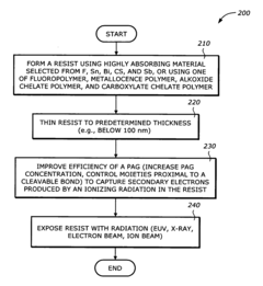
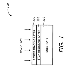
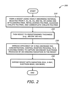
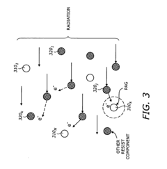
Absorptive resists in an extreme ultraviolet (EUV) imaging layer
PatentInactiveUS20050069818A1
Innovation
- The use of highly absorptive resist formulations with EUV-absorbing moieties like fluorine or tin, combined with increased Photo Acid Generator (PAG) concentration and controlled moieties to capture secondary electrons, allows for increased sensitivity without worsening LER, achieved by forming an ultra-thin imaging layer with balanced thickness and absorption.
Environmental Impact of EUV Resist Processing
The environmental impact of EUV resist processing represents a critical consideration in the semiconductor industry's sustainability efforts. Traditional photoresist processes involve significant chemical usage, including developers, rinse solutions, and various solvents that can contribute to environmental pollution. EUV resist processing, while offering technological advantages in lithography resolution, introduces unique environmental challenges that must be systematically evaluated and addressed.
EUV resist formulations typically contain metal-based components that enhance absorption and quantum efficiency, such as hafnium, zirconium, or tin. These metals, while beneficial for lithographic performance, raise concerns regarding their potential environmental persistence and toxicity. Waste streams containing these materials require specialized treatment protocols to prevent contamination of water systems and soil. Current data indicates that approximately 70-80% of resist material becomes waste during processing, highlighting the significance of this environmental burden.
Energy consumption represents another substantial environmental impact factor in EUV resist processing. The EUV lithography systems themselves require considerable power for operation, with estimates suggesting energy requirements 3-5 times higher than traditional deep ultraviolet (DUV) systems. This increased energy demand translates to a larger carbon footprint unless powered by renewable energy sources. Additionally, the precise temperature control required for optimal resist performance further contributes to energy consumption throughout the manufacturing process.
Water usage in EUV resist processing presents both challenges and opportunities for environmental improvement. While the process requires ultra-pure water for development and rinsing stages, recent innovations have focused on reducing water consumption through recycling systems and more efficient rinsing techniques. Some advanced facilities have reported water usage reductions of up to 30% compared to earlier generation processes, though industry-wide implementation remains inconsistent.
Airborne emissions from EUV resist processing also warrant careful consideration. Volatile organic compounds (VOCs) and particulate matter may be released during various processing stages, particularly during baking and development. Modern fabrication facilities typically employ advanced air filtration and abatement systems, but the unique chemistry of EUV resists may require specialized treatment approaches to ensure complete capture of potential contaminants.
Regulatory frameworks governing EUV resist processing continue to evolve globally, with increasing emphasis on lifecycle assessment and circular economy principles. The European Union's REACH regulations and similar initiatives in Asia and North America are driving manufacturers toward greener chemistry approaches, including the development of more environmentally benign EUV resist formulations with comparable absorption and quantum efficiency characteristics.
Integration Challenges with Advanced Node Manufacturing
The integration of EUV lithography into advanced node manufacturing processes presents significant challenges that require careful consideration and innovative solutions. As semiconductor technology continues to advance toward smaller nodes (5nm and below), the evaluation of EUV absorption and quantum efficiency in resists becomes increasingly critical for successful integration.
One of the primary integration challenges involves the compatibility between EUV resists and existing manufacturing infrastructure. While EUV lithography offers superior resolution capabilities, the transition from traditional 193nm immersion lithography requires substantial modifications to process flows, equipment configurations, and material handling protocols. These modifications must account for the unique properties of EUV resists, particularly their absorption characteristics and quantum efficiency parameters.
Pattern collapse represents another significant integration challenge at advanced nodes. As feature sizes decrease, the aspect ratio of resist patterns increases, making them more susceptible to collapse during development and subsequent processing steps. This issue is exacerbated by the inherent properties of EUV resists, which must balance sensitivity, resolution, and mechanical stability. The quantum efficiency of these resists directly impacts the energy required for pattern formation, which in turn affects the mechanical integrity of resulting structures.
Line edge roughness (LER) and line width roughness (LWR) become increasingly problematic at advanced nodes. The stochastic nature of EUV absorption and photon shot noise contributes significantly to these issues. Manufacturing integration must address these fundamental physical limitations through optimized resist formulations, process conditions, and potentially complementary techniques such as directed self-assembly or multi-patterning strategies.
Defectivity control presents another critical integration challenge. EUV resists must demonstrate exceptional cleanliness and uniformity to prevent pattern defects that can render devices non-functional. The evaluation of absorption characteristics and quantum efficiency must therefore include considerations for defect formation mechanisms, including those related to photochemical reactions, material inhomogeneities, and processing variations.
Metrology and inspection capabilities must also evolve to support EUV resist integration. Traditional optical inspection techniques face limitations when evaluating sub-10nm features, necessitating advanced metrology solutions that can accurately characterize resist performance parameters, including absorption profiles and quantum efficiency metrics across wafer surfaces.
Finally, cost considerations remain a significant integration challenge. The economic viability of advanced node manufacturing depends on achieving acceptable throughput and yield metrics. EUV resist performance directly impacts exposure times, process windows, and defect rates, all of which contribute to overall manufacturing costs. Optimizing quantum efficiency and absorption characteristics therefore represents not just a technical challenge but an economic imperative for successful integration into high-volume manufacturing environments.
Unlock deeper insights with Patsnap Eureka Quick Research — get a full tech report to explore trends and direct your research. Try now!
Generate Your Research Report Instantly with AI Agent
Supercharge your innovation with Patsnap Eureka AI Agent Platform!